ML5238
16 series Li-ion secondary battery protection, Analog Front End IC
FEDL5238-05
Issue date: Jan. 22, 2014
GENERAL DESCRIPTION
The ML5238 is analog front end IC for 16 series Lithium Ion secondary battery pack protection system. The
ML5238 provides the function of cell voltage monitoring, charge/discharge current monitoring function, and it
can detect over-charge/over-discharge of each battery cell charge/discharge over-current.
The ML5238 has short current detecting function which can turn off the external charge/discharge MOS-FET
without external MCU.
FEATURES
• 16 cell highly accurate voltage monitoring function: output cell voltage by half from VMON pin
• built-in cell balancing switches for each cell
• charge/discharge current monitoring function :
Select voltage gain of ISP-ISM and output from IMON pin.
Voltage gain selection: x10 / x50
ISP-ISM voltage = 0.1V/0.2V/0.3V/0.4V (typ),
the detecting delay time is set by external capacitor
• short current detecting function: detecting threshold voltage is selectable,
• external charge/discharge FET control: NMOS-FET driver built-in
• MCU interface: SPI serial interface (mode 0)
• 3.3V regulator for external MCU built-in: output current is 10mA (max)
• Reference voltage regulator for external ADC: 3.3V(typ), 3.28V(min),3.34V(max) @Ta=-10°C to +60°C
• Small power consumption
: 50µA (typ), 100µA (max)
: 25µA (typ), 50µA (max)
: 0.1µA (typ), 1µA (max)
: +7V to +80V
: -40°C to +85°C
: 44 pin plastic QFP (QFP44-P-910-0.80-2K)
Normal state
Power save state
Power down state
• power supply voltage
• operating temperature
• package
Note: The ML5238 is forbidden to be used for automotive or any equipment, device or system which
requires an extremely high level of reliability and quality, such as a medical instrument,
transportation equipment, aerospace machinery, nuclear-reactor controller, fuel-controller or
other safety device. If whether product is intended to be used for any such special purpose is
difficult to be decided, please contact a ROHM sales representative before purchasing.
Confidential
1/30
�
VREF
VREG
Voltage
Regulator
VDD
VDDP
s
e
h
c
t
i
VDD SW
w
S
e
c
n
a
l
a
B
l
l
e
C
&
n
o
i
t
c
e
l
e
S
V16
V15
V14
V13
V12
V11
V10
V9
V8
V7
V6
V5
V4
V3
V2
V1
V0
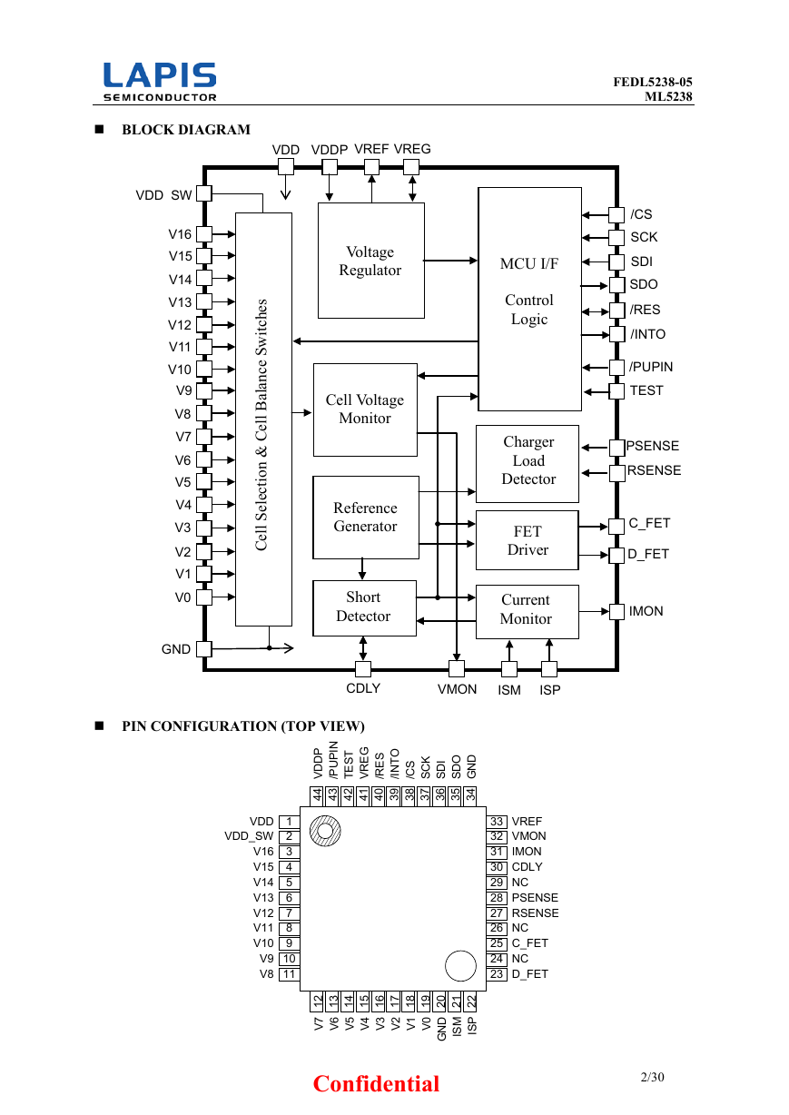
BLOCK DIAGRAM
PIN CONFIGURATION (TOP VIEW)
VDD
VDD_SW
V16
V15
V14
V13
V12
V11
V10
V9
V8
1
2
3
4
5
6
7
8
9
10
11
l
l
e
C
GND
N
P
U
P
P
D
D
V
T
S
E
T
/
I
Cell Voltage
Monitor
Reference
Generator
Short
Detector
CDLY
FEDL5238-05
ML5238
/CS
SCK
SDI
SDO
/RES
/INTO
/PUPIN
TEST
PSENSE
RSENSE
C_FET
D_FET
IMON
MCU I/F
Control
Logic
Charger
Load
Detector
FET
Driver
Current
Monitor
VMON
ISM
ISP
G
E
R
V
S
E
R
/
O
T
N
I
/
K
C
S
I
D
S
O
D
S
D
N
G
S
C
/
4
4
3
4
2
4
1
4
0
4
9
3
8
3
7
3
6
3
5
3
4
3
33
32
31
30
29
28
27
26
25
24
23
VREF
VMON
IMON
CDLY
NC
PSENSE
RSENSE
NC
C_FET
NC
D_FET
2/30
2
1
3
1
4
1
5
1
6
1
7
1
8
1
9
1
0
2
1
2
2
2
M
S
I
P
S
I
7
V
6
V
5
V
4
V
3
V
2
V
1
V
0
V
D
N
G
Confidential
�
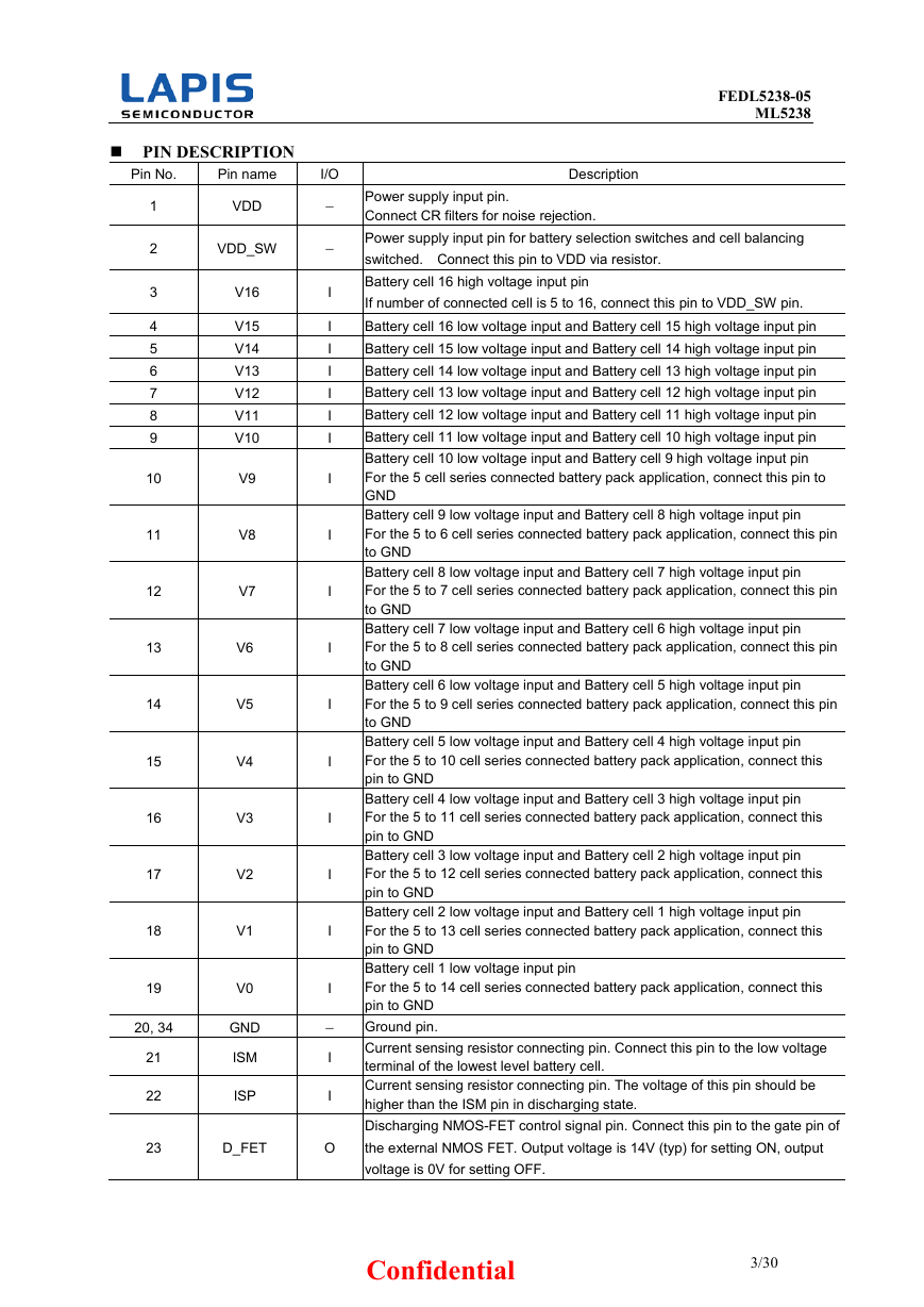
PIN DESCRIPTION
Pin name
Pin No.
1
2
3
4
5
6
7
8
9
10
11
12
13
14
15
16
17
18
19
VDD
VDD_SW
V16
V15
V14
V13
V12
V11
V10
V9
V8
V7
V6
V5
V4
V3
V2
V1
V0
20, 34
21
22
23
GND
ISM
ISP
D_FET
FEDL5238-05
ML5238
I/O
−
−
I
I
I
I
I
I
I
I
I
I
I
I
I
I
I
I
I
−
I
I
O
Description
Power supply input pin.
Connect CR filters for noise rejection.
Power supply input pin for battery selection switches and cell balancing
switched. Connect this pin to VDD via resistor.
Battery cell 16 high voltage input pin
If number of connected cell is 5 to 16, connect this pin to VDD_SW pin.
Battery cell 16 low voltage input and Battery cell 15 high voltage input pin
Battery cell 15 low voltage input and Battery cell 14 high voltage input pin
Battery cell 14 low voltage input and Battery cell 13 high voltage input pin
Battery cell 13 low voltage input and Battery cell 12 high voltage input pin
Battery cell 12 low voltage input and Battery cell 11 high voltage input pin
Battery cell 11 low voltage input and Battery cell 10 high voltage input pin
Battery cell 10 low voltage input and Battery cell 9 high voltage input pin
For the 5 cell series connected battery pack application, connect this pin to
GND
Battery cell 9 low voltage input and Battery cell 8 high voltage input pin
For the 5 to 6 cell series connected battery pack application, connect this pin
to GND
Battery cell 8 low voltage input and Battery cell 7 high voltage input pin
For the 5 to 7 cell series connected battery pack application, connect this pin
to GND
Battery cell 7 low voltage input and Battery cell 6 high voltage input pin
For the 5 to 8 cell series connected battery pack application, connect this pin
to GND
Battery cell 6 low voltage input and Battery cell 5 high voltage input pin
For the 5 to 9 cell series connected battery pack application, connect this pin
to GND
Battery cell 5 low voltage input and Battery cell 4 high voltage input pin
For the 5 to 10 cell series connected battery pack application, connect this
pin to GND
Battery cell 4 low voltage input and Battery cell 3 high voltage input pin
For the 5 to 11 cell series connected battery pack application, connect this
pin to GND
Battery cell 3 low voltage input and Battery cell 2 high voltage input pin
For the 5 to 12 cell series connected battery pack application, connect this
pin to GND
Battery cell 2 low voltage input and Battery cell 1 high voltage input pin
For the 5 to 13 cell series connected battery pack application, connect this
pin to GND
Battery cell 1 low voltage input pin
For the 5 to 14 cell series connected battery pack application, connect this
pin to GND
Ground pin.
Current sensing resistor connecting pin. Connect this pin to the low voltage
terminal of the lowest level battery cell.
Current sensing resistor connecting pin. The voltage of this pin should be
higher than the ISM pin in discharging state.
Discharging NMOS-FET control signal pin. Connect this pin to the gate pin of
the external NMOS FET. Output voltage is 14V (typ) for setting ON, output
voltage is 0V for setting OFF.
Confidential
3/30
�
FEDL5238-05
ML5238
Pin No.
Pin name
I/O
Description
25
27
28
30
31
32
33
35
36
37
38
39
40
41
42
43
44
24, 26, 29
NC
C_FET
RSENSE
PSENSE
CDLY
IMON
VMON
VREF
SDO
SDI
SCK
/CS
/INTO
O
I
I
IO
O
O
O
O
I
I
I
O
/RES
IO
VREG
TEST
/PUPIN
VDDP
O
I
I
−
−
Charging NMOS-FET control signal output pin. Connect this pin to the gate
pin of the external NMOS FET. Output voltage is 14V (typ) for setting ON,
output is Hi-Z for setting OFF.
Input pin for detecting the load disconnection. Connect this pin to the
negative side of the load.
Input pin for detecting the charger disconnection. Connect this pin to the
negative side of the charger. If charger is connected to the same node as
the load, connect this pin to the RSENSE pin.
Short current detection delay time setting pin. Connect a capacitor between
GND and this pin.
Current monitor output pin. The voltage amplified the voltage between
ISP-ISM by 10 or 50 is outputted. When current is not flowing, 1V (typ) is
outputted.
Cell voltage monitor output pin. The voltage amplified a cell voltage by 0.5
is outputted.
Reference voltage output (3.3V) for external ADC. Connect a 4.7µF capacitor
between this pin and the GND pin.
Serial interface data output pin. If /CS input is “H”, output of this pin is Hi-Z
state.
Serial interface data input pin.
Serial interface clock input pin. Capture the SDI input at the rising edge of
the SCK clock. Output the data from the SDO pin at the falling edge of the
SCK.
Serial interface chip select pin. The serial interface is active if the input is
“L”.
Interrupt signal output to external MCU. This pin is a NMOS open drain
output pin and output is “L” level if interrupted.
Reset signal input and a reset signal output to external MCU. Since this pin is
a NMOS open drain output pin, connect a 0.1µF capacitor between this pin
and GND pin and pull-up resisitor. When recovered power-down state, ”L”
level reset pulse will be outputted and both ML5238 and external MCU will be
initialized.
Built-in 3.3V regulator output pin. Connect a 4.7µF capacitor between this pin
and GND pin. It can be used as a power supply to the external MCU. And it is
also used as a power supply to the MCU interface circuit in this IC.
Test input pin. Fix to GND level.
Power-up trigger input pin. If input is “L” level, the state of the ML5238
changes from power-down state to Initial state. A 100kΩ pull-up resistor is
built-in between this pin and the VDD pin.
Power supply input pin for internal regulator.
Connect CR filters for noise rejection.
No connection pin. Open this pin.
Confidential
4/30
�
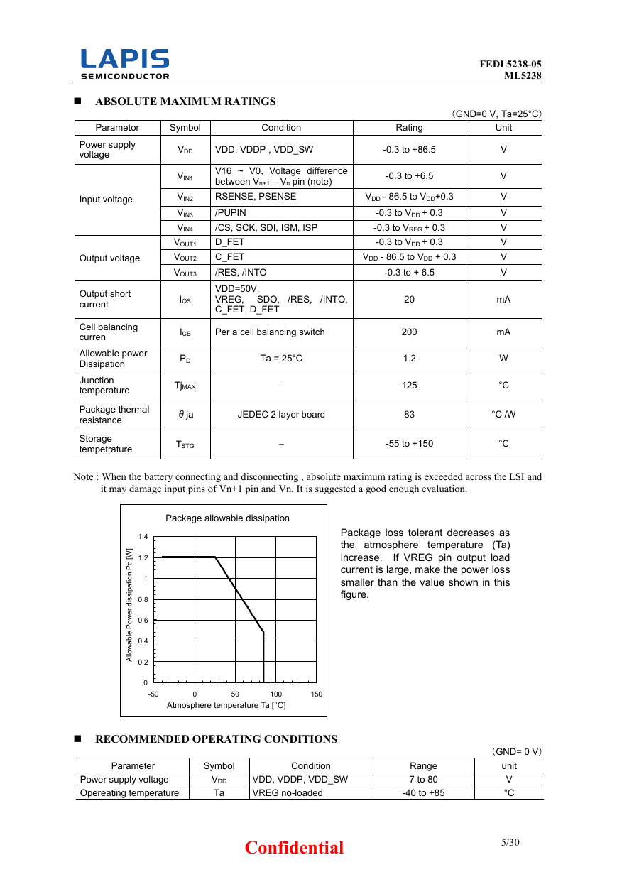
ABSOLUTE MAXIMUM RATINGS
FEDL5238-05
ML5238
(GND=0 V, Ta=25°C)
Parametor
Power supply
voltage
Input voltage
Output voltage
Output short
current
Cell balancing
curren
Allowable power
Dissipation
Junction
temperature
Package thermal
resistance
Storage
tempetrature
Symbol
Condition
Rating
Unit
VDD
VDD, VDDP , VDD_SW
-0.3 to +86.5
VIN1
VIN2
VIN3
VIN4
VOUT1
VOUT2
VOUT3
IOS
ICB
PD
TjMAX
θja
TSTG
V16 ~ V0, Voltage difference
between Vn+1 – Vn pin (note)
RSENSE, PSENSE
/PUPIN
/CS, SCK, SDI, ISM, ISP
D_FET
C_FET
/RES, /INTO
VDD=50V,
VREG, SDO,
C_FET, D_FET
/INTO,
/RES,
Per a cell balancing switch
Ta = 25°C
−
JEDEC 2 layer board
-0.3 to +6.5
VDD - 86.5 to VDD+0.3
-0.3 to VDD + 0.3
-0.3 to VREG + 0.3
-0.3 to VDD + 0.3
VDD - 86.5 to VDD + 0.3
-0.3 to + 6.5
20
200
1.2
125
83
−
-55 to +150
V
V
V
V
V
V
V
V
mA
mA
W
°C
°C /W
°C
Note : When the battery connecting and disconnecting , absolute maximum rating is exceeded across the LSI and
it may damage input pins of Vn+1 pin and Vn. It is suggested a good enough evaluation.
Parameter
Power supply voltage
Opereating temperature
Symbol
VDD
Ta
Condition
VDD, VDDP, VDD_SW
VREG no-loaded
Range
7 to 80
-40 to +85
Confidential
(GND= 0 V)
unit
V
°C
5/30
Package loss tolerant decreases as
the atmosphere
temperature (Ta)
increase. If VREG pin output load
current is large, make the power loss
smaller than the value shown in this
figure.
1.4
1
.
]
W
i
i
1.2
0.8
0.6
[
d
P
n
o
i
t
a
p
s
s
d
Package allowable dissipation
RECOMMENDED OPERATING CONDITIONS
100
Atmosphere temperature Ta [°C]
0
-50
r
e
w
o
P
e
b
a
w
o
l
l
l
150
0.4
0.2
0
50
A
�
Parameter
Symbol
Condition
Min.
Typ.
VDD=7 to 80V,GND=0 V,Ta=-40 to +85°C,VREG output no-loaded
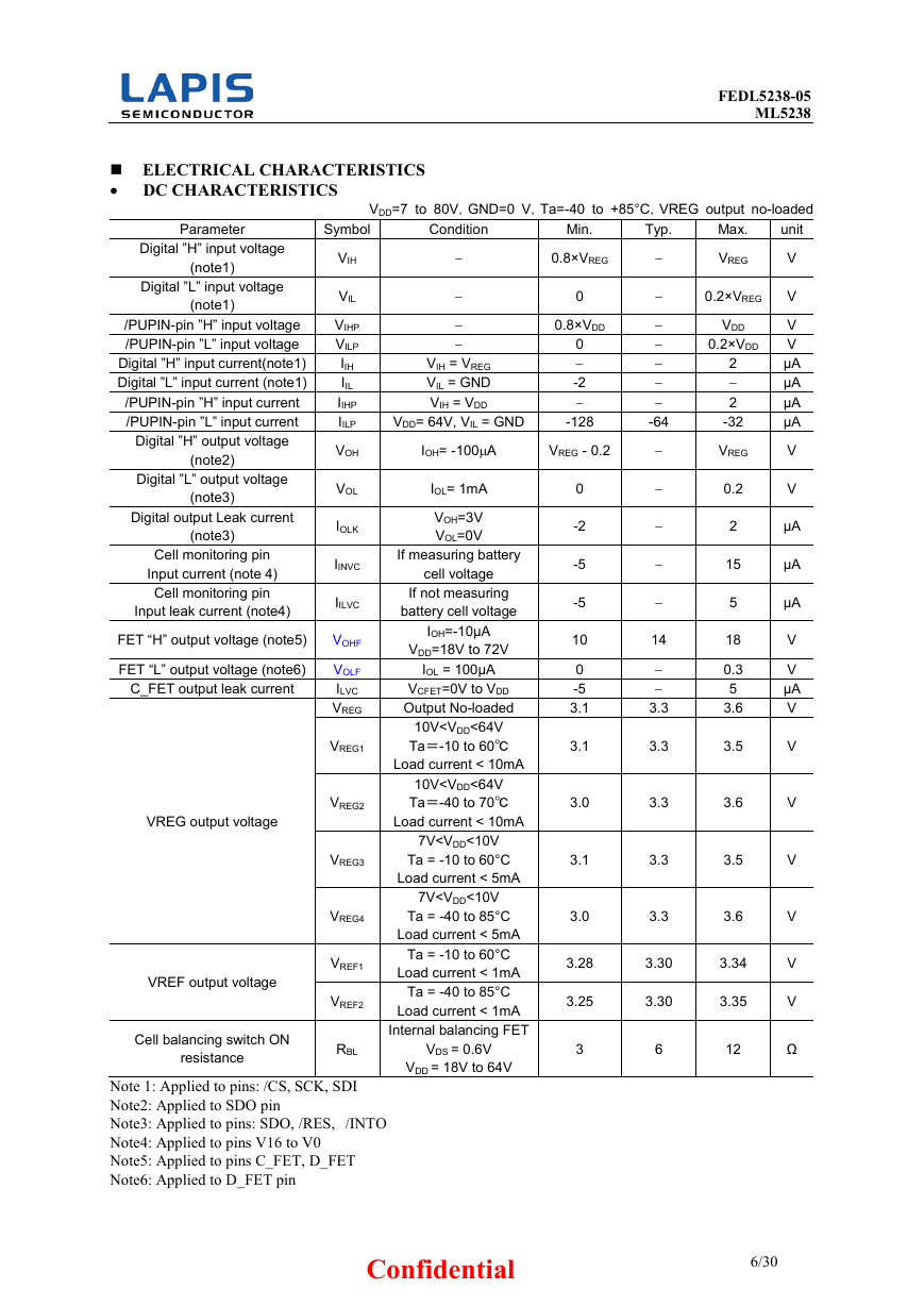
ELECTRICAL CHARACTERISTICS
• DC CHARACTERISTICS
Digital ”H” input voltage
(note1)
Digital ”L” input voltage
(note1)
/PUPIN-pin ”H” input voltage
/PUPIN-pin ”L” input voltage
Digital ”H” input current(note1)
Digital ”L” input current (note1)
/PUPIN-pin ”H” input current
/PUPIN-pin ”L” input current
Digital ”H” output voltage
(note2)
Digital ”L” output voltage
(note3)
Digital output Leak current
(note3)
Cell monitoring pin
Input current (note 4)
Cell monitoring pin
Input leak current (note4)
FET “H” output voltage (note5)
FET “L” output voltage (note6)
C_FET output leak current
VREG output voltage
VREF output voltage
Cell balancing switch ON
resistance
VIH
VIL
VIHP
VILP
IIH
IIL
IIHP
IILP
VOH
VOL
IOLK
IINVC
IILVC
VOHF
VOLF
ILVC
VREG
VREG1
VREG2
VREG3
VREG4
VREF1
VREF2
RBL
−
−
−
−
VIH = VREG
VIL = GND
VIH = VDD
0.8×VREG
0
0.8×VDD
0
−
-2
−
VDD= 64V, VIL = GND
-128
IOH= -100µA
VREG - 0.2
IOL= 1mA
VOH=3V
VOL=0V
If measuring battery
cell voltage
If not measuring
battery cell voltage
IOH=-10µA
VDD=18V to 72V
IOL = 100µA
VCFET=0V to VDD
Output No-loaded
10V
•
FEDL5238-05
ML5238
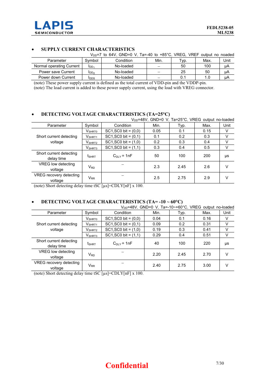
SUPPLY CURRENT CHARACTERISTICS
VDD=7 to 64V,GND=0 V,Ta=-40 to +85°C,VREG, VREF output no noaded
Parameter
Symbol
Normal operating Current
Power save Current
Power down Current
IDD1
IDD2
IDDS
Condition
No-loaded
No-loaded
No-loaded
Min.
−
−
−
Typ.
50
25
0.1
Max.
100
50
1.0
Unit
µA
µA
µA
(note) These power supply current is defined as the total current of VDD-pin and the VDDP-pin.
(note) The load current is added to these power supply current, using the load with VREG connector.
• DETECTING VOLTAGE CHARACTERISTICS (TA=25°C)
Parameter
Short current detecting
voltage
Short current detecting
delay time
VREG low detecting
voltage
VREG recovery detecting
voltage
VDD=48V,GND=0 V,Ta=25°C,VREG output no-loaded
Symbol
VSHRT0
VSHRT1
VSHRT2
VSHRT3
tSHRT
VRD
VRR
Condition
SC1,SC0 bit = (0,0)
SC1,SC0 bit = (0,1)
SC1,SC0 bit = (1,0)
SC1,SC0 bit = (1,1)
CDLY = 1nF
−
−
Min.
0.05
0.1
0.2
0.3
50
2.3
2.5
Typ.
0.1
0.2
0.3
0.4
100
2.45
2.75
Max.
0.15
0.3
0.4
0.5
200
2.6
2.9
Unit
V
V
V
V
µs
V
V
(note) Short detecting delay time tSC [µs]=CDLY[nF] x 100.
• DETECTING VOLTAGE CHARACTERISTICS (TA= -10 ~ 60°C)
VDD=48V,GND=0 V,Ta=-10~+60°C,VREG output no-loaded
Symbol
VSHRT0
VSHRT1
VSHRT2
VSHRT3
tSHRT
VRD
VRR
Condition
SC1,SC0 bit = (0,0)
SC1,SC0 bit = (0,1)
SC1,SC0 bit = (1,0)
SC1,SC0 bit = (1,1)
CDLY = 1nF
−
−
Min.
0.04
0.09
0.19
0.29
40
2.20
2.40
Typ.
0.1
0.2
0.3
0.4
100
2.45
2.75
Max.
0.16
0.31
0.41
0.51
220
2.70
3.00
Unit
V
V
V
V
µs
V
V
Parameter
Short current detecting
voltage
Short current detecting
delay time
VREG low detecting
voltage
VREG recovery detecting
voltage
(note) Short detecting delay time tSC [µs]=CDLY[nF] x 100.
Confidential
7/30
�
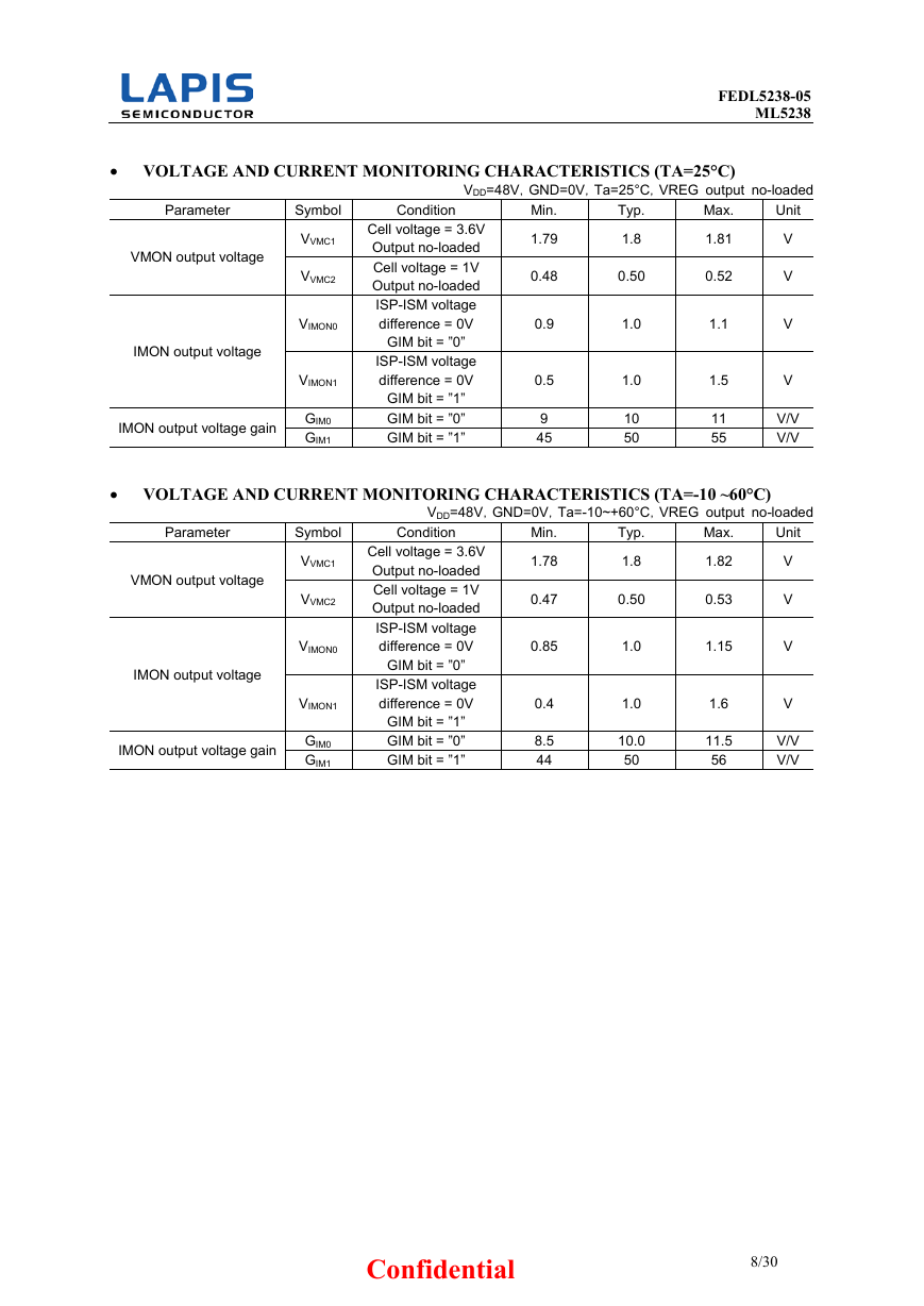
• VOLTAGE AND CURRENT MONITORING CHARACTERISTICS (TA=25°C)
FEDL5238-05
ML5238
VDD=48V,GND=0V,Ta=25°C,VREG output no-loaded
Parameter
VMON output voltage
IMON output voltage
IMON output voltage gain
Symbol
VVMC1
VVMC2
VIMON0
VIMON1
GIM0
GIM1
Condition
Cell voltage = 3.6V
Output no-loaded
Cell voltage = 1V
Output no-loaded
ISP-ISM voltage
difference = 0V
GIM bit = ”0”
ISP-ISM voltage
difference = 0V
GIM bit = ”1”
GIM bit = ”0”
GIM bit = ”1”
Min.
1.79
0.48
0.9
0.5
Typ.
1.8
0.50
1.0
1.0
Max.
1.81
0.52
1.1
1.5
9
45
10
50
11
55
Unit
V
V
V
V
V/V
V/V
• VOLTAGE AND CURRENT MONITORING CHARACTERISTICS (TA=-10 ~60°C)
VDD=48V,GND=0V,Ta=-10~+60°C,VREG output no-loaded
Parameter
VMON output voltage
IMON output voltage
IMON output voltage gain
Symbol
VVMC1
VVMC2
VIMON0
VIMON1
GIM0
GIM1
Condition
Cell voltage = 3.6V
Output no-loaded
Cell voltage = 1V
Output no-loaded
ISP-ISM voltage
difference = 0V
GIM bit = ”0”
ISP-ISM voltage
difference = 0V
GIM bit = ”1”
GIM bit = ”0”
GIM bit = ”1”
Min.
1.78
0.47
0.85
0.4
8.5
44
Typ.
1.8
0.50
1.0
1.0
10.0
50
Max.
1.82
0.53
1.15
1.6
11.5
56
Unit
V
V
V
V
V/V
V/V
Confidential
8/30
�



 2023年江西萍乡中考道德与法治真题及答案.doc
 2012年重庆南川中考生物真题及答案.doc
 2013年江西师范大学地理学综合及文艺理论基础考研真题.doc
 2020年四川甘孜小升初语文真题及答案I卷.doc
 2020年注册岩土工程师专业基础考试真题及答案.doc
 2023-2024学年福建省厦门市九年级上学期数学月考试题及答案.doc
 2021-2022学年辽宁省沈阳市大东区九年级上学期语文期末试题及答案.doc
 2022-2023学年北京东城区初三第一学期物理期末试卷及答案.doc
 2018上半年江西教师资格初中地理学科知识与教学能力真题及答案.doc
 2012年河北国家公务员申论考试真题及答案-省级.doc
 2020-2021学年江苏省扬州市江都区邵樊片九年级上学期数学第一次质量检测试题及答案.doc
 2022下半年黑龙江教师资格证中学综合素质真题及答案.doc