logo资料库

Arm Debug Interface Architecture Specification ADIv6.0.pdf

第1页 / 共402页
第2页 / 共402页
第3页 / 共402页
第4页 / 共402页
第5页 / 共402页
第6页 / 共402页
第7页 / 共402页
第8页 / 共402页
资料共402页,剩余部分请下载后查看
Arm Debug Interface Architecture Specification ADIv6.0
Contents
Preface
About this manual
Intended audience
Using this book
Conventions
Typographic conventions
Signals
Timing diagrams
Numbers
Pseudocode descriptions
Additional reading
Arm publications
Other publications
Feedback
Feedback on this book
Part A: The Arm Debug Interface
A1: About the Arm Debug Interface
A1.1 ADI versions
A1.2 Purpose of the ADI
A1.2.1 Embedded core debug functionality
A1.2.2 System debug functionality
A1.2.3 Compatibility between CoreSight and Arm debug interfaces
A1.3 The debug link
A1.4 The subdivisions of an ADIv6 implementation
A1.4.1 Connections to the ADI
A1.4.2 Accessing the DP and AP registers
A1.5 The Debug Port (DP)
A1.6 Access Ports (APs)
A1.6.1 Using the Debug Port to access Access Ports
A1.6.2 Guide to the detailed description of a MEM-AP
A1.6.3 Guide to the detailed description of a JTAG-AP
A1.6.4 Using the AP to access debug resources
A1.7 Design choices and implementation examples
A1.7.1 Choices for the DP
A1.7.2 Choices for the APs
A1.8 Power Requests
Part B: The Debug Port
B1: About the DP
B1.1 MINDP, Minimal DP extension
B1.2 Sticky flags and DP error responses
B1.3 The transaction counter
B1.4 Pushed-compare and pushed-verify operations
B1.5 Power and reset control
B2: DP Reference Information
B2.1 DP architecture versions
B2.1.1 DP architecture versions summary
B2.1.2 DP architecture version 3 (DPv3) address map
B2.1.3 Register maps, and accesses to reserved addresses
B2.2 DP register descriptions
B2.2.1 ABORT, Abort register
B2.2.2 BASEPTR0-BASEPTR1, Base Pointer 0 and 1
B2.2.3 CTRL/STAT, Control/Status register
B2.2.4 DLCR, Data Link Control Register
B2.2.5 DLPIDR, Data Link Protocol Identification Register
B2.2.6 DPIDR, Debug Port Identification Register
B2.2.7 DPIDR1, Debug Port Identification Register 1
B2.2.8 EVENTSTAT, Event Status register
B2.2.9 RDBUFF, Read Buffer register
B2.2.10 RESEND, Read Resend register
B2.2.11 SELECT-SELECT1, AP Select registers
B2.2.12 TARGETID, Target Identification register
B2.2.13 TARGETSEL, Target Selection register
B2.3 System and debug power control behavior
B2.3.1 The ADI power domains model
B2.3.2 Power control requirements and operation
B2.3.3 Emulation of powerdown
B2.3.4 Emulation of power control
B2.4 Debug reset control behavior
B2.4.1 Emulation of debug reset request
B2.4.2 Limitations of CDBGRSTREQ and CDBGRSTACK
B2.5 System reset control behavior
B2.5.1 Limitations of system reset control
B3: The JTAG Debug Port (JTAG-DP)
B3.1 About the JTAG-DP
B3.2 The scan chain interface
B3.2.1 DP elements
B3.2.2 Physical connection to the JTAG-DP
B3.2.3 The Debug TAP State Machine (DBGTAPSM)
B3.3 IR scan chain and IR instructions
B3.3.1 Required IR instructions
B3.3.2 IMPLEMENTATION DEFINED extensions to the IR instruction set
B3.3.3 IR, JTAG-DP Instruction Register
B3.4 DR scan chain and DR instructions
B3.4.1 ABORT, JTAG-DP Abort register
B3.4.2 BYPASS, JTAG-DP Bypass register
B3.4.3 DPACC and APACC, JTAG-DP DP and AP Access registers
B3.4.4 IDCODE, the JTAG TAP ID register
B4: The Serial Wire Debug Port (SW-DP)
B4.1 About the SWD protocol
B4.1.1 Basic operation
B4.1.2 SWD protocol versions
B4.1.3 Line turnaround
B4.1.4 Idle cycles
B4.1.5 Bit order
B4.1.6 Parity
B4.1.7 Limitations of multi-drop
B4.2 SWD protocol operation
B4.2.1 Successful write operation (OK response)
B4.2.2 Successful read operation (OK response)
B4.2.3 WAIT response to read or write operation request
B4.2.4 FAULT response to read or write operation request
B4.2.5 Protocol error response
B4.2.6 Sticky overrun behavior
B4.2.7 SW-DP write buffering
B4.2.8 Summary of target responses
B4.2.9 Summary of host responses
B4.3 SWD interface
B4.3.1 Line interface
B4.3.2 Line pull-up
B4.3.3 Connection and line reset sequence
B4.3.4 Target selection protocol, SWD protocol version 2
B5: The Serial Wire/JTAG Debug Port (SWJ-DP)
B5.1 About the SWJ-DP
B5.1.1 SWJ-DP structure
B5.1.2 Limitations when reusing pins
B5.2 Switching between SWD and JTAG
B5.2.1 The Switching Mechanism
B5.2.2 Switching from JTAG to SWD operation
B5.2.3 Switching from SWD to JTAG operation
B5.3 Dormant operation
B5.3.1 Using the dormant state outside of SWJ-DP
B5.3.2 Switching from JTAG to dormant state
B5.3.3 Switching from SWD to dormant state
B5.3.4 Leaving dormant state
B5.4 Restrictions on switching between operating modes
Part C: The Access Port
C1: About the AP
C1.1 AP requirements
C1.2 Selecting and accessing an AP
C1.2.1 Stalling accesses
C1.3 AP Programmers’ Model Summary
C1.4 AP Register Descriptions
C1.4.1 AUTHSTATUS, Authentication Status Register
C1.4.2 CIDR0-CIDR3, Component Identification Registers
C1.4.3 CLAIMSET and CLAIMCLR, Claim Tag Set Register and Claim Tag Clear Register
C1.4.4 DEVAFF0-DEVAFF1, Device Affinity Registers
C1.4.5 DEVARCH, Device Architecture Register
C1.4.6 DEVID, Device Configuration Register
C1.4.7 DEVID1-DEVID2, Device Configuration Registers
C1.4.8 DEVTYPE, Device Type Register
C1.4.9 IDR, Identification Register
C1.4.10 ITCTRL, Integration Mode Control Register
C1.4.11 LAR and LSR, Lock Access Register and Lock Status Register
C1.4.12 PIDR0-PIDR7, Peripheral Identification Registers
C2: The Memory Access Port (MEM-AP)
C2.1 About the MEM-AP
C2.1.1 The programmers’ model for debug register access
C2.1.2 Selecting and accessing the MEM-AP
C2.1.3 The MEM-AP registers
C2.1.4 MEM-AP register accesses and memory accesses
C2.1.5 MEM-AP response to an abort request through the DP ABORT register
C2.2 MEM-AP functions
C2.2.1 Enabling access to the connected debug device or memory system
C2.2.2 Auto-incrementing the Transfer Address Register (TAR)
C2.2.3 Stalling accesses
C2.2.4 Error Handling
C2.2.5 Response to debug component errors
C2.2.6 Variable access size for memory accesses
C2.2.7 Byte lanes
C2.2.8 Packed transfers
C2.2.9 Slave Memory Ports
C2.2.10 Twin MEM-APs
C2.2.11 Software access control
C2.3 Implementing a MEM-AP
C2.3.1 IMPLEMENTATION DEFINED features of a MEM-AP implementation
C2.3.2 MEM-AP implementation requirements
C2.3.3 MEM-AP Extensions
C2.4 MEM-AP examples of pushed-verify and pushed-compare
C2.4.1 Example of using a pushed-verify operation on a MEM-AP
C2.4.2 Example of using a pushed-find operation on a MEM-AP
C2.4.3 Example of using the transaction counter for a pushed-compare operation on a MEM-AP
C2.5 MEM-AP Programmers’ Model
C2.6 MEM-AP register descriptions
C2.6.1 AUTHSTATUS, Authentication Status Register
C2.6.2 BASE, Debug Base Address register
C2.6.3 BD0-BD3, Banked Data registers
C2.6.4 CFG, Configuration register
C2.6.5 CIDR0-CIDR3, Component Identification Registers
C2.6.6 CLAIMSET and CLAIMCLR, Claim Tag Set Register and Claim Tag Clear Register
C2.6.7 CSW, Control/Status Word register
C2.6.8 DAR0-DAR255, Direct Access registers
C2.6.9 DEVAFF0-DEVAFF1, Device Affinity Registers
C2.6.10 DEVARCH, Device Architecture Register
C2.6.11 DEVID, Device Configuration Register
C2.6.12 DEVID1-DEVID2, Device Configuration Registers
C2.6.13 DEVTYPE, Device Type Register
C2.6.14 DRW, Data Read/Write register
C2.6.15 IDR, Identification Register
C2.6.16 ITCTRL, Integration Mode Control Register
C2.6.17 LAR and LSR, Lock Access Register and Lock Status Register
C2.6.18 MBT, Memory Barrier Transfer register
C2.6.19 PIDR0-PIDR7, Peripheral Identification Register
C2.6.20 TAR, Transfer Address Register
C2.6.21 TRR, Transfer Response register
C3: The JTAG Access Port (JTAG-AP)
C3.1 About the JTAG-AP
C3.1.1 Selecting and accessing the JTAG-AP
C3.1.2 Logical structure of the JTAG-AP
C3.1.3 JTAG port signals
C3.2 Operation of the JTAG-AP
C3.2.1 Stalling accesses
C3.2.2 Resetting connected JTAG devices or subsystems
C3.2.3 Handling of an ABORT instruction
C3.2.4 Pushed transaction and transaction counter support
C3.3 The JTAG Engine Byte Command Protocol
C3.3.1 The encoding of the TMS packet
C3.3.2 The encoding of the TDI_TDO packet
C3.3.3 Response bytes from a TDI_TDO packet
C3.4 JTAG-AP programmers’ model
C3.5 JTAG-AP register descriptions
C3.5.1 AUTHSTATUS, Authentication Status Register
C3.5.2 BRFIFO1-BRFIFO4, Byte FIFO registers for read access
C3.5.3 BWFIFO1-BWFIFO4, Byte FIFO registers for write access
C3.5.4 CIDR0-CIDR3, Component Identification Registers
C3.5.5 CLAIMSET and CLAIMCLR, Claim Tag Set Register and Claim Tag Clear Register
C3.5.6 CSW, Control/Status Word Register
C3.5.7 DEVAFF0-DEVAFF1, Device Affinity Registers
C3.5.8 DEVARCH, Device Architecture Register
C3.5.9 DEVID, Device Configuration Register
C3.5.10 DEVID1-DEVID2, Device Configuration Registers
C3.5.11 DEVTYPE, Device Type Register
C3.5.12 ITCTRL, Integration Mode Control Register
C3.5.13 LAR and LSR, Lock Access Register and Lock Status Register
C3.5.14 PIDR0-PIDR7, Peripheral Identification Register
C3.5.15 PSEL, Port Select register
C3.5.16 PSTA, Port Status Register
Part D: Identification Registers and ROM Tables
D1: Component and Peripheral ID Registers
D1.1 About the Component and Peripheral ID registers
D1.2 Component and Peripheral Identification Registers Reference Information
D1.2.1 CIDR0-CIDR3, Component Identification Registers
D1.2.2 PIDR0-PIDR7, Peripheral Identification Registers
D1.3 Legacy Peripheral ID layout
D2: About ROM Tables
D2.1 ROM Tables Overview
D2.2 ROM Table Types
D2.3 Component and Peripheral ID Registers for ROM Tables
D2.3.1 Identifying the debug SoC or platform
D2.4 The component address
D2.5 Location of the ROM Table
D2.6 ROM Table hierarchies
D2.6.1 Peripheral ID Registers in lower-level ROM Tables
D2.6.2 Component Revision Numbers
D2.6.3 Prohibited ROM Table references
D3: Class 0x1 ROM Tables
D3.1 About Class 0x1 ROM Tables
D3.2 Class 0x1 ROM Table summary
D3.2.1 Class 0x1 ROM Table Layout
D3.2.2 ROM Table entries that are marked not present
D3.3 Use of power domain IDs
D3.3.1 Power domain entries
D3.3.2 Algorithm to discover power domain IDs
D3.4 Register Descriptions
D3.4.1 CIDR0-CIDR3, Component Identification Registers
D3.4.2 MEMTYPE, Memory Type Register
D3.4.3 PIDR0-PIDR7, Peripheral Identification Register
D3.4.4 ROMENTRY, Class 0x1 ROM Table entries
D4: Class 0x9 ROM Tables
D4.1 About Class 0x9 ROM Tables
D4.2 Class 0x9 ROM Table summary
D4.2.1 Class 0x9 ROM Table Layout
D4.2.2 ROM Table entries that are marked not present
D4.3 Use of power domain IDs
D4.3.1 Power domain entries
D4.3.2 Algorithm to discover power domain IDs
D4.3.3 Debug power requests
D4.3.4 System power requests
D4.4 Reset control
D4.4.1 Debug reset control
D4.4.2 System reset control
D4.5 Register descriptions
D4.5.1 AUTHSTATUS, Authentication Status Register
D4.5.2 CIDR0-CIDR3, Component Identification Registers
D4.5.3 CLAIMSET and CLAIMCLR, Claim Tag Set Register and Claim Tag Clear Register
D4.5.4 DBGPCR, Debug Power Control Registers
D4.5.5 DBGPSR, Debug Power Status Registers
D4.5.6 DBGRSTAR, Debug Reset Acknowledge Register
D4.5.7 DBGRSTRR, Debug Reset Request Register
D4.5.8 DEVAFF0-DEVAFF1, Device Affinity Registers
D4.5.9 DEVARCH, Device Architecture Register
D4.5.10 DEVID, Device Configuration Register
D4.5.11 DEVID1-DEVID2, Device Configuration Registers
D4.5.12 DEVTYPE, Device Type Register
D4.5.13 ITCTRL, Integration Mode Control Register
D4.5.14 LAR and LSR, Software Lock Access Register and Software Lock Status Register
D4.5.15 PIDR0-PIDR7, Peripheral Identification Register
D4.5.16 PRIDR0, Power Request ID Register 0
D4.5.17 ROMENTRY, Class 0x9 ROM Table entries
D4.5.18 SYSPCR, Debug Power Control Registers
D4.5.19 SYSPSR, System Power Status Registers
D4.5.20 SYSRSTAR, System Reset Acknowledge Register
D4.5.21 SYSRSTRR, System Reset Request Register
Part E: Appendixes
E1: Standard Memory Access Port Definitions
E1.1 Introduction
E1.2 AMBA AXI3 and AXI4
E1.2.1 CSW register implementation
E1.3 AMBA AXI4 with ACE-Lite
E1.3.1 CSW register implementation
E1.3.2 MBT register implementation
E1.4 AMBA AHB3
E1.4.1 CSW register implementation
E1.5 AMBA AHB5
E1.5.1 CSW register implementation
E1.6 AMBA APB2 and APB3
E1.6.1 CSW register implementation
E1.7 AMBA APB4
E1.7.1 CSW register implementation
E2: Cross-over with the Arm Architecture
E2.1 Introduction
E2.2 Armv6-M, Armv7-M, and Armv8-M architecture profiles
E2.3 Armv7-A without Large Physical Address Extension, Armv7-R, and Armv8-R
E2.4 Armv7-A with Large Physical Address Extension, and Armv8-A
E2.5 Summary of the requirements for ADIv6 implementations
E3: Pseudocode Definition
E3.1 About Arm pseudocode
E3.1.1 General limitations of Arm pseudocode
E3.2 Data types
E3.2.1 General data type rules
E3.2.2 Bitstrings
E3.2.3 Integers
E3.2.4 Reals
E3.2.5 Booleans
E3.2.6 Enumerations
E3.2.7 Lists
E3.2.8 Arrays
E3.3 Expressions
E3.3.1 General expression syntax
E3.3.2 Operators and functions - polymorphism and prototypes
E3.3.3 Precedence rules
E3.4 Operators and built-in functions
E3.4.1 Operations on generic types
E3.4.2 Operations on Booleans
E3.4.3 Bitstring manipulation
E3.4.4 Arithmetic
E3.5 Statements and program structure
E3.5.1 Simple statements
E3.5.2 Compound statements
E3.5.3 Comments
E4: Revisions
Glossary
Arm® Debug Interface Architecture Specification ADIv6.0 Copyright © 2018 Arm Limited or its affiliates. All rights reserved. ARM IHI 0074B (ID042618)
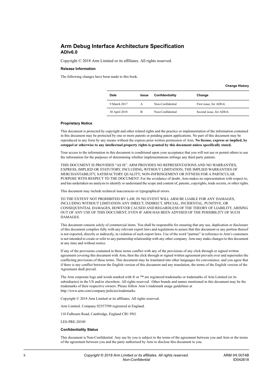
Arm Debug Interface Architecture Specification ADIv6.0 Copyright © 2018 Arm Limited or its affiliates. All rights reserved. Release Information The following changes have been made to this book. Date Issue Confidentiality Change 9 March 2017 30 April 2018 A B Non-Confidential Non-Confidential First issue, for ADIv6. Second issue, for ADIv6. Change History Proprietary Notice This document is protected by copyright and other related rights and the practice or implementation of the information contained in this document may be protected by one or more patents or pending patent applications. No part of this document may be reproduced in any form by any means without the express prior written permission of Arm. No license, express or implied, by estoppel or otherwise to any intellectual property rights is granted by this document unless specifically stated. Your access to the information in this document is conditional upon your acceptance that you will not use or permit others to use the information for the purposes of determining whether implementations infringe any third party patents. THIS DOCUMENT IS PROVIDED “AS IS”. ARM PROVIDES NO REPRESENTATIONS AND NO WARRANTIES, EXPRESS, IMPLIED OR STATUTORY, INCLUDING, WITHOUT LIMITATION, THE IMPLIED WARRANTIES OF MERCHANTABILITY, SATISFACTORY QUALITY, NON-INFRINGEMENT OR FITNESS FOR A PARTICULAR PURPOSE WITH RESPECT TO THE DOCUMENT. For the avoidance of doubt, Arm makes no representation with respect to, and has undertaken no analysis to identify or understand the scope and content of, patents, copyrights, trade secrets, or other rights. This document may include technical inaccuracies or typographical errors. TO THE EXTENT NOT PROHIBITED BY LAW, IN NO EVENT WILL ARM BE LIABLE FOR ANY DAMAGES, INCLUDING WITHOUT LIMITATION ANY DIRECT, INDIRECT, SPECIAL, INCIDENTAL, PUNITIVE, OR CONSEQUENTIAL DAMAGES, HOWEVER CAUSED AND REGARDLESS OF THE THEORY OF LIABILITY, ARISING OUT OF ANY USE OF THIS DOCUMENT, EVEN IF ARM HAS BEEN ADVISED OF THE POSSIBILITY OF SUCH DAMAGES. This document consists solely of commercial items. You shall be responsible for ensuring that any use, duplication or disclosure of this document complies fully with any relevant export laws and regulations to assure that this document or any portion thereof is not exported, directly or indirectly, in violation of such export laws. Use of the word “partner” in reference to Arm’s customers is not intended to create or refer to any partnership relationship with any other company. Arm may make changes to this document at any time and without notice. If any of the provisions contained in these terms conflict with any of the provisions of any click through or signed written agreement covering this document with Arm, then the click through or signed written agreement prevails over and supersedes the conflicting provisions of these terms. This document may be translated into other languages for convenience, and you agree that if there is any conflict between the English version of this document and any translation, the terms of the English version of the Agreement shall prevail. The Arm corporate logo and words marked with ® or ™ are registered trademarks or trademarks of Arm Limited (or its subsidiaries) in the US and/or elsewhere. All rights reserved. Other brands and names mentioned in this document may be the trademarks of their respective owners. Please follow Arm’s trademark usage guidelines at http://www.arm.com/company/policies/trademarks. Copyright © 2018 Arm Limited or its affiliates. All rights reserved. Arm Limited. Company 02557590 registered in England. 110 Fulbourn Road, Cambridge, England CB1 9NJ. LES-PRE-20349 Confidentiality Status This document is Non-Confidential. Any use by you is subject to the terms of the agreement between you and Arm or the terms of the agreement between you and the party authorised by Arm to disclose this document to you. ii Copyright © 2018 Arm Limited or its affiliates. All rights reserved. Non-Confidential ARM IHI 0074B ID042618
Product Status The information in this document is final, that is for a developed product. Web Address http://www.arm.com ARM IHI 0074B ID042618 Copyright © 2018 Arm Limited or its affiliates. All rights reserved. Non-Confidential iii
iv Copyright © 2018 Arm Limited or its affiliates. All rights reserved. Non-Confidential ARM IHI 0074B ID042618
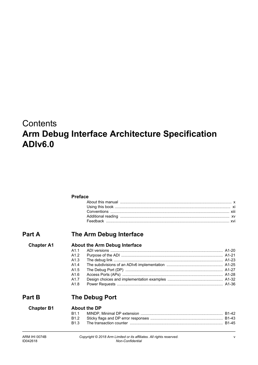
Contents Arm Debug Interface Architecture Specification ADIv6.0 Preface About this manual ....................................................................................................... x Using this book ........................................................................................................... xi Conventions .............................................................................................................. xiii Additional reading ..................................................................................................... xv Feedback .................................................................................................................. xvi The Arm Debug Interface About the Arm Debug Interface A1.1 A1.2 A1.3 A1.4 A1.5 A1.6 A1.7 A1.8 ADI versions ........................................................................................................ A1-20 Purpose of the ADI .............................................................................................. A1-21 The debug link ..................................................................................................... A1-23 The subdivisions of an ADIv6 implementation .................................................... A1-25 The Debug Port (DP) .......................................................................................... A1-27 Access Ports (APs) ............................................................................................. A1-28 Design choices and implementation examples ................................................... A1-32 Power Requests .................................................................................................. A1-36 The Debug Port About the DP B1.1 B1.2 B1.3 MINDP, Minimal DP extension ............................................................................ B1-42 Sticky flags and DP error responses ................................................................... B1-43 The transaction counter ...................................................................................... B1-45 Part A Chapter A1 Part B Chapter B1 ARM IHI 0074B ID042618 Copyright © 2018 Arm Limited or its affiliates. All rights reserved. Non-Confidential v
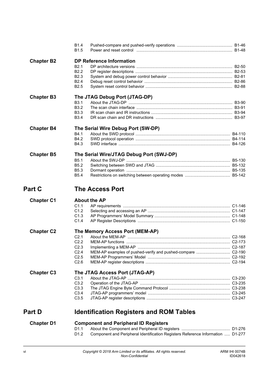
Chapter B2 Chapter B3 Chapter B4 Chapter B5 Part C Chapter C1 Chapter C2 Chapter C3 B1.4 B1.5 Pushed-compare and pushed-verify operations ................................................. B1-46 Power and reset control ..................................................................................... B1-48 DP Reference Information B2.1 B2.2 B2.3 B2.4 B2.5 DP architecture versions ..................................................................................... B2-50 DP register descriptions ...................................................................................... B2-53 System and debug power control behavior ......................................................... B2-81 Debug reset control behavior .............................................................................. B2-86 System reset control behavior ............................................................................. B2-88 The JTAG Debug Port (JTAG-DP) B3.1 B3.2 B3.3 B3.4 About the JTAG-DP ............................................................................................ B3-90 The scan chain interface ..................................................................................... B3-91 IR scan chain and IR instructions ........................................................................ B3-94 DR scan chain and DR instructions .................................................................... B3-97 The Serial Wire Debug Port (SW-DP) B4.1 B4.2 B4.3 About the SWD protocol .................................................................................... B4-110 SWD protocol operation .................................................................................... B4-114 SWD interface ................................................................................................... B4-126 The Serial Wire/JTAG Debug Port (SWJ-DP) B5.1 B5.2 B5.3 B5.4 About the SWJ-DP ............................................................................................ B5-130 Switching between SWD and JTAG .................................................................. B5-132 Dormant operation ............................................................................................ B5-135 Restrictions on switching between operating modes ........................................ B5-142 The Access Port About the AP C1.1 C1.2 C1.3 C1.4 AP requirements ............................................................................................... C1-146 Selecting and accessing an AP ......................................................................... C1-147 AP Programmers’ Model Summary ................................................................... C1-148 AP Register Descriptions .................................................................................. C1-150 The Memory Access Port (MEM-AP) C2.1 C2.2 C2.3 C2.4 C2.5 C2.6 About the MEM-AP ........................................................................................... C2-168 MEM-AP functions ............................................................................................ C2-173 Implementing a MEM-AP .................................................................................. C2-187 MEM-AP examples of pushed-verify and pushed-compare .............................. C2-190 MEM-AP Programmers’ Model ......................................................................... C2-192 MEM-AP register descriptions ........................................................................... C2-194 The JTAG Access Port (JTAG-AP) C3.1 C3.2 C3.3 C3.4 C3.5 About the JTAG-AP ........................................................................................... C3-230 Operation of the JTAG-AP ................................................................................ C3-235 The JTAG Engine Byte Command Protocol ...................................................... C3-238 JTAG-AP programmers’ model ......................................................................... C3-245 JTAG-AP register descriptions .......................................................................... C3-247 Part D Chapter D1 Identification Registers and ROM Tables Component and Peripheral ID Registers D1.1 D1.2 About the Component and Peripheral ID registers ........................................... D1-276 Component and Peripheral Identification Registers Reference Information ..... D1-277 vi Copyright © 2018 Arm Limited or its affiliates. All rights reserved. Non-Confidential ARM IHI 0074B ID042618
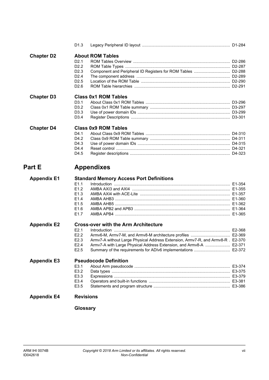
Chapter D2 Chapter D3 Chapter D4 Part E Appendix E1 Appendix E2 Appendix E3 D1.3 Legacy Peripheral ID layout .............................................................................. D1-284 About ROM Tables D2.1 D2.2 D2.3 D2.4 D2.5 D2.6 ROM Tables Overview ...................................................................................... D2-286 ROM Table Types ............................................................................................. D2-287 Component and Peripheral ID Registers for ROM Tables ................................ D2-288 The component address ................................................................................... D2-289 Location of the ROM Table ............................................................................... D2-290 ROM Table hierarchies ..................................................................................... D2-291 Class 0x1 ROM Tables D3.1 D3.2 D3.3 D3.4 About Class 0x1 ROM Tables ........................................................................... D3-296 Class 0x1 ROM Table summary ....................................................................... D3-297 Use of power domain IDs .................................................................................. D3-299 Register Descriptions ........................................................................................ D3-301 Class 0x9 ROM Tables D4.1 D4.2 D4.3 D4.4 D4.5 About Class 0x9 ROM Tables ........................................................................... D4-310 Class 0x9 ROM Table summary ....................................................................... D4-311 Use of power domain IDs .................................................................................. D4-315 Reset control ..................................................................................................... D4-321 Register descriptions ......................................................................................... D4-323 Appendixes Standard Memory Access Port Definitions E1.1 E1.2 E1.3 E1.4 E1.5 E1.6 E1.7 Introduction ....................................................................................................... E1-354 AMBA AXI3 and AXI4 ....................................................................................... E1-355 AMBA AXI4 with ACE-Lite ................................................................................ E1-357 AMBA AHB3 ...................................................................................................... E1-360 AMBA AHB5 ...................................................................................................... E1-362 AMBA APB2 and APB3 ..................................................................................... E1-364 AMBA APB4 ...................................................................................................... E1-365 Cross-over with the Arm Architecture E2.1 E2.2 E2.3 E2.4 E2.5 Introduction ....................................................................................................... E2-368 Armv6-M, Armv7-M, and Armv8-M architecture profiles ................................... E2-369 Armv7-A without Large Physical Address Extension, Armv7-R, and Armv8-R . E2-370 Armv7-A with Large Physical Address Extension, and Armv8-A ...................... E2-371 Summary of the requirements for ADIv6 implementations ................................ E2-372 Pseudocode Definition E3.1 E3.2 E3.3 E3.4 E3.5 About Arm pseudocode ..................................................................................... E3-374 Data types ......................................................................................................... E3-375 Expressions ....................................................................................................... E3-379 Operators and built-in functions ........................................................................ E3-381 Statements and program structure .................................................................... E3-386 Appendix E4 Revisions Glossary ARM IHI 0074B ID042618 Copyright © 2018 Arm Limited or its affiliates. All rights reserved. Non-Confidential vii
viii Copyright © 2018 Arm Limited or its affiliates. All rights reserved. Non-Confidential ARM IHI 0074B ID042618
分享到:
收藏