Rev 5; 7/10
®
♦
♦
♦
♦
♦
♦
♦
♦
°°
♦
VCC
μC
RPUP
IO
DS28E01-100
GND
PART
DS28E01P-100+
DS28E01P-100+T
DS28E01G-100+T&R
TEMP RANGE
-40°C to +85°C
-40°C to +85°C
-40°C to +85°C
DS28E01Q-100+T&R
-40°C to +85°C
PIN-PACKAGE
6 TSOC
6 TSOC
2 SFN
6 TDFN-EP*
(2.5k pcs)
+
*
本文是英文数据资料的译文,文中可能存在翻译上的不准确或错误。如需进一步确认,请在您的设计中参考英文资料。有关价格、供货及订购信息,请联络Maxim亚洲销售中心:10800 852 1249 (北中国区),10800 152 1249 (南中国区),或访问Maxim的中文网站:china.maximintegrated.com。AVAILABLEDS28E01-100�
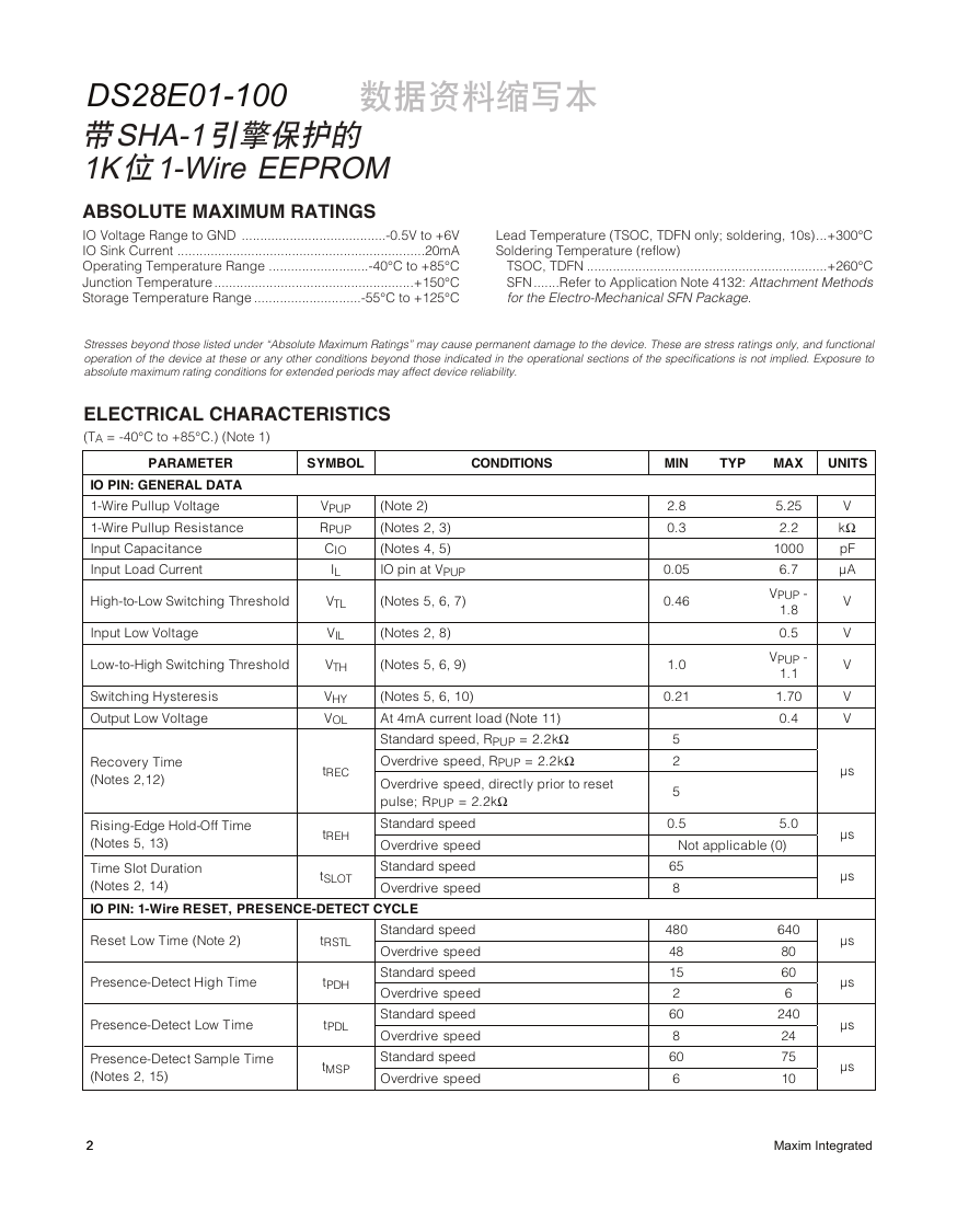
ABSOLUTE MAXIMUM RATINGS
IO Voltage Range to GND .......................................-0.5V to +6V
IO Sink Current ...................................................................20mA
Operating Temperature Range ...........................-40°C to +85°C
Junction Temperature......................................................+150°C
Storage Temperature Range .............................-55°C to +125°C
Lead Temperature (TSOC, TDFN only; soldering, 10s)...+300°C
Soldering Temperature (reflow)
TSOC, TDFN .................................................................+260°C
SFN .......Refer to Application Note 4132: Attachment Methods
for the Electro-Mechanical SFN Package.
Stresses beyond those listed under “Absolute Maximum Ratings” may cause permanent damage to the device. These are stress ratings only, and functional
operation of the device at these or any other conditions beyond those indicated in the operational sections of the specifications is not implied. Exposure to
absolute maximum rating conditions for extended periods may affect device reliability.
ELECTRICAL CHARACTERISTICS
(TA = -40°C to +85°C.) (Note 1)
SYMBOL
CONDITIONS
MIN
TYP
MAX
UNITS
PARAMETER
IO PIN: GENERAL DATA
1-Wire Pullup Voltage
1-Wire Pullup Resistance
Input Capacitance
Input Load Current
High-to-Low Switching Threshold
Input Low Voltage
Low-to-High Switching Threshold
Switching Hysteresis
Output Low Voltage
Recovery Time
(Notes 2,12)
Rising-Edge Hold-Off Time
(Notes 5, 13)
VPUP
RPUP
CIO
IL
VTL
VIL
VTH
VHY
VOL
tREC
tREH
(Note 2)
(Notes 2, 3)
(Notes 4, 5)
IO pin at VPUP
(Notes 5, 6, 7)
(Notes 2, 8)
(Notes 5, 6, 9)
(Notes 5, 6, 10)
At 4mA current load (Note 11)
Standard speed, RPUP = 2.2k
Overdrive speed, RPUP = 2.2k
Overdrive speed, directly prior to reset
pulse; RPUP = 2.2k
Standard speed
Overdrive speed
Standard speed
Overdrive speed
2.8
0.3
0.05
0.46
1.0
0.21
5
2
5
0.5
5.25
2.2
1000
6.7
VPUP -
1.8
0.5
VPUP -
1.1
1.70
0.4
5.0
Not applicable (0)
65
8
V
k
pF
μA
V
V
V
V
V
μs
μs
μs
μs
μs
μs
μs
Time Slot Duration
(Notes 2, 14)
IO PIN: 1-Wire RESET, PRESENCE-DETECT CYCLE
tSLOT
Reset Low Time (Note 2)
Presence-Detect High Time
Presence-Detect Low Time
Presence-Detect Sample Time
(Notes 2, 15)
tRSTL
tPDH
tPDL
tMSP
Standard speed
Overdrive speed
Standard speed
Overdrive speed
Standard speed
Overdrive speed
Standard speed
Overdrive speed
480
48
15
2
60
8
60
6
640
80
60
6
240
24
75
10
DS28E01-1002Maxim Integrated2�
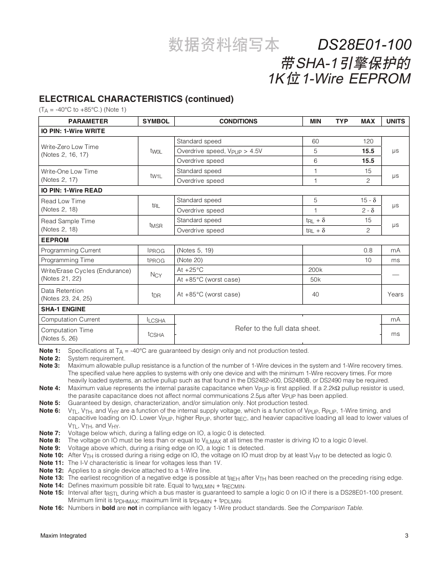
ELECTRICAL CHARACTERISTICS (continued)
(TA = -40°C to +85°C.) (Note 1)
PARAMETER
SYMBOL
CONDITIONS
MIN
TYP
MAX
UNITS
IO PIN: 1-Wire WRITE
Write-Zero Low Time
(Notes 2, 16, 17)
Write-One Low Time
(Notes 2, 17)
IO PIN: 1-Wire READ
Read Low Time
(Notes 2, 18)
Read Sample Time
(Notes 2, 18)
EEPROM
Programming Current
Programming Time
Write/Erase Cycles (Endurance)
(Notes 21, 22)
Data Retention
(Notes 23, 24, 25)
SHA-1 ENGINE
Computation Current
Computation Time
(Notes 5, 26)
tW0L
tW1L
tRL
tMSR
Standard speed
Overdrive speed, VPUP > 4.5V
Overdrive speed
Standard speed
Overdrive speed
Standard speed
Overdrive speed
Standard speed
Overdrive speed
IPROG
tPROG
NCY
(Notes 5, 19)
(Note 20)
At +25°C
At +85°C (worst case)
tDR
At +85°C (worst case)
60
5
6
1
1
5
1
tRL +
tRL +
200k
50k
40
ILCSHA
tCSHA
Refer to the full data sheet.
120
15.5
15.5
15
2
15 -
2 -
15
2
0.8
10
μs
μs
μs
μs
mA
ms
Years
mA
ms
Note 1:
Note 2:
Note 3: Maximum allowable pullup resistance is a function of the number of 1-Wire devices in the system and 1-Wire recovery times.
Specifications at TA = -40°C are guaranteed by design only and not production tested.
System requirement.
The specified value here applies to systems with only one device and with the minimum 1-Wire recovery times. For more
heavily loaded systems, an active pullup such as that found in the DS2482-x00, DS2480B, or DS2490 may be required.
Note 4: Maximum value represents the internal parasite capacitance when VPUP is first applied. If a 2.2kΩ pullup resistor is used,
the parasite capacitance does not affect normal communications 2.5μs after VPUP has been applied.
Note 5: Guaranteed by design, characterization, and/or simulation only. Not production tested.
Note 6:
VTL, VTH, and VHY are a function of the internal supply voltage, which is a function of VPUP, RPUP, 1-Wire timing, and
capacitive loading on IO. Lower VPUP, higher RPUP, shorter tREC, and heavier capacitive loading all lead to lower values of
VTL, VTH, and VHY.
Voltage below which, during a falling edge on IO, a logic 0 is detected.
The voltage on IO must be less than or equal to VILMAX at all times the master is driving IO to a logic 0 level.
Voltage above which, during a rising edge on IO, a logic 1 is detected.
Note 7:
Note 8:
Note 9:
Note 10: After VTH is crossed during a rising edge on IO, the voltage on IO must drop by at least VHY to be detected as logic 0.
Note 11: The I-V characteristic is linear for voltages less than 1V.
Note 12: Applies to a single device attached to a 1-Wire line.
Note 13: The earliest recognition of a negative edge is possible at tREH after VTH has been reached on the preceding rising edge.
Note 14: Defines maximum possible bit rate. Equal to tW0LMIN + tRECMIN.
Note 15:
Interval after tRSTL during which a bus master is guaranteed to sample a logic 0 on IO if there is a DS28E01-100 present.
Minimum limit is tPDHMAX; maximum limit is tPDHMIN + tPDLMIN.
Note 16: Numbers in bold are not in compliance with legacy 1-Wire product standards. See the Comparison Table.
Maxim Integrated3DS28E01-100�
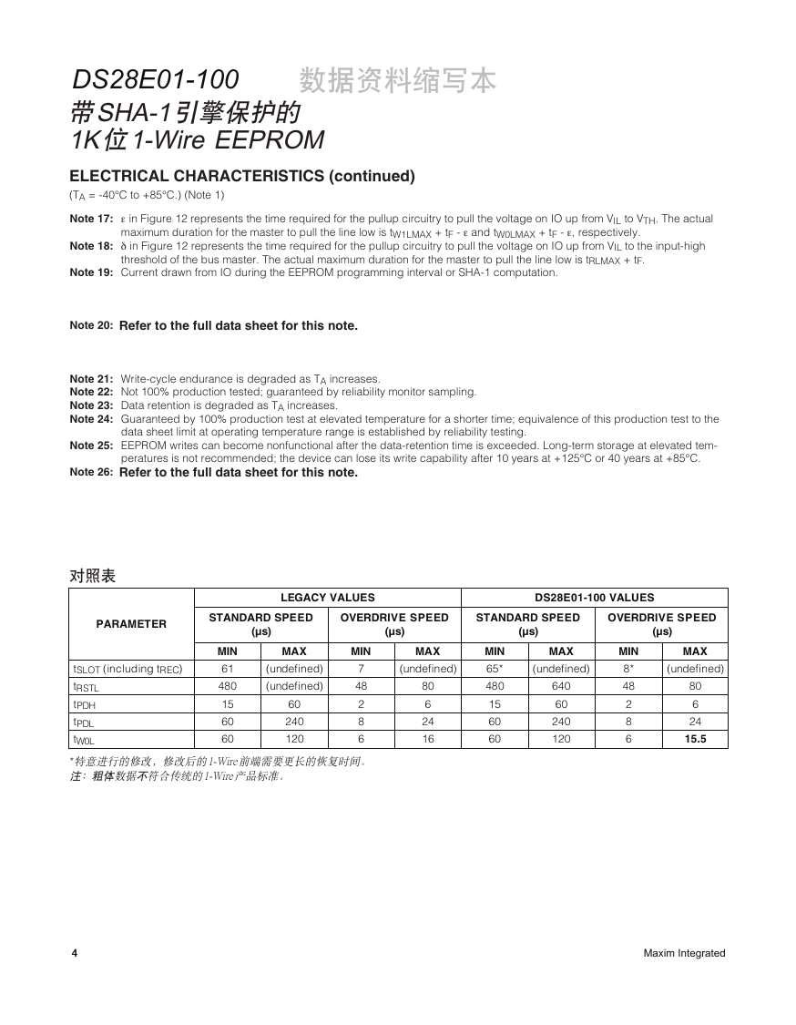
ELECTRICAL CHARACTERISTICS (continued)
(TA = -40°C to +85°C.) (Note 1)
Note 17: ε in Figure 12 represents the time required for the pullup circuitry to pull the voltage on IO up from VIL to VTH. The actual
maximum duration for the master to pull the line low is tW1LMAX + tF - ε and tW0LMAX + tF - ε, respectively.
Note 18: δ in Figure 12 represents the time required for the pullup circuitry to pull the voltage on IO up from VIL to the input-high
threshold of the bus master. The actual maximum duration for the master to pull the line low is tRLMAX + tF.
Note 19: Current drawn from IO during the EEPROM programming interval or SHA-1 computation.
Note 20:
Refer to the full data sheet for this note.
Note 21: Write-cycle endurance is degraded as TA increases.
Note 22: Not 100% production tested; guaranteed by reliability monitor sampling.
Note 23: Data retention is degraded as TA increases.
Note 24: Guaranteed by 100% production test at elevated temperature for a shorter time; equivalence of this production test to the
data sheet limit at operating temperature range is established by reliability testing.
Note 25: EEPROM writes can become nonfunctional after the data-retention time is exceeded. Long-term storage at elevated tem-
Note 26:
peratures is not recommended; the device can lose its write capability after 10 years at +125°C or 40 years at +85°C.
Refer to the full data sheet for this note.
LEGACY VALUES
DS28E01-100 VALUES
PARAMETER
STANDARD SPEED
OVERDRIVE SPEED
STANDARD SPEED
OVERDRIVE SPEED
(μs)
(μs)
(μs)
(μs)
tSLOT (including tREC)
tRSTL
tPDH
tPDL
tW0L
MIN
61
480
15
60
60
MAX
MIN
MAX
(undefined)
(undefined)
60
240
120
7
48
2
8
6
(undefined)
80
6
24
16
MIN
65*
480
15
60
60
MAX
(undefined)
640
60
240
120
MIN
8*
48
2
8
6
MAX
(undefined)
80
6
24
15.5
*
DS28E01-1004Maxim Integrated4�
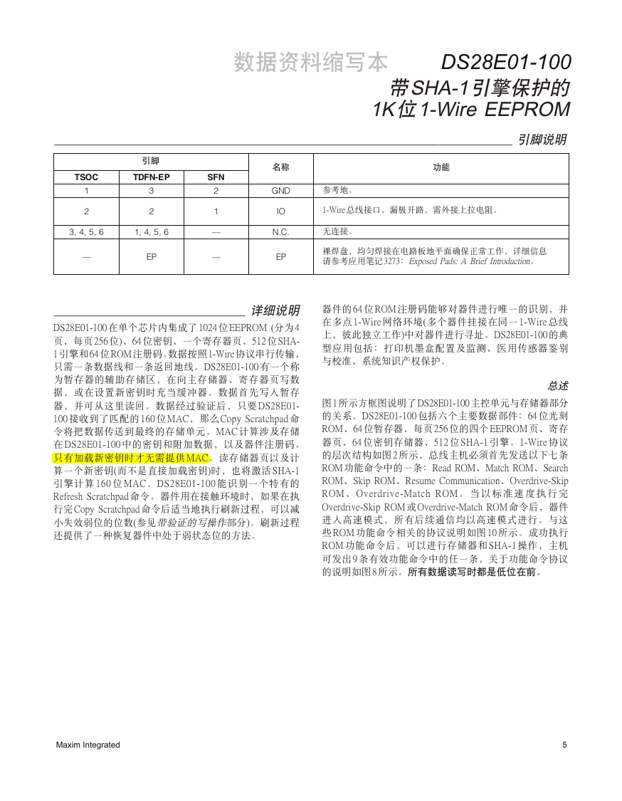
TSOC
TDFN-EP
SFN
1
2
3
2
3, 4, 5, 6
1, 4, 5, 6
—
EP
2
1
—
—
GND
IO
N.C.
EP
Maxim Integrated5DS28E01-100�
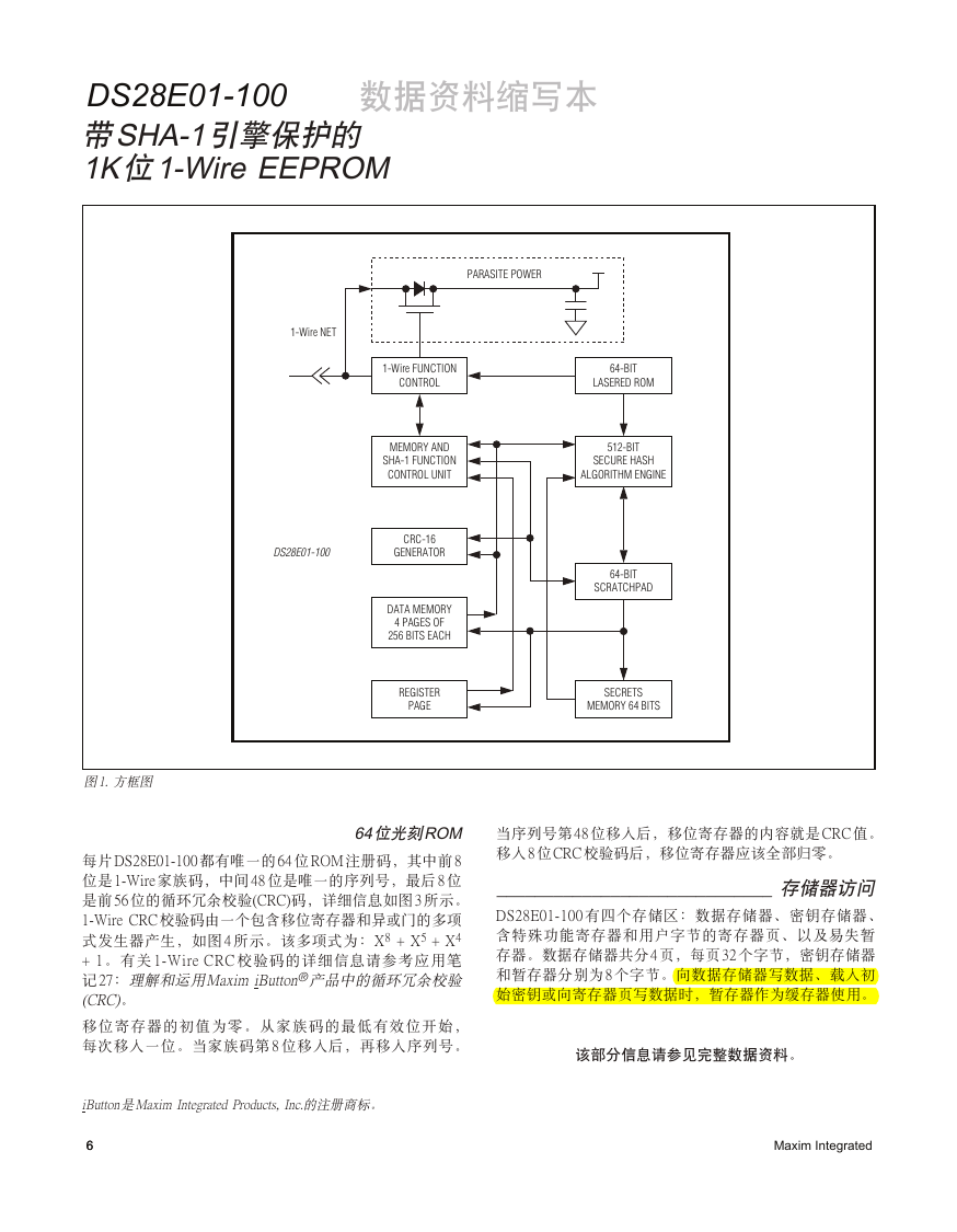
PARASITE POWER
1-Wire NET
1-Wire FUNCTION
CONTROL
64-BIT
LASERED ROM
MEMORY AND
SHA-1 FUNCTION
CONTROL UNIT
DS28E01-100
CRC-16
GENERATOR
DATA MEMORY
4 PAGES OF
256 BITS EACH
REGISTER
PAGE
512-BIT
SECURE HASH
ALGORITHM ENGINE
64-BIT
SCRATCHPAD
SECRETS
MEMORY 64 BITS
®
DS28E01-1006Maxim Integrated6�
COMMAND LEVEL:
AVAILABLE COMMANDS:
DATA FIELD AFFECTED:
DS28E01-100
1-Wire ROM FUNCTION COMMANDS
(SEE FIGURE 10)
READ ROM
MATCH ROM
SEARCH ROM
SKIP ROM
RESUME
OVERDRIVE-SKIP ROM
OVERDRIVE-MATCH ROM
64-BIT REG. #, RC-FLAG
64-BIT REG. #, RC-FLAG
64-BIT REG. #, RC-FLAG
RC-FLAG
RC-FLAG
RC-FLAG, OD-FLAG
64-BIT REG. #, RC-FLAG, OD-FLAG
DEVICE-SPECIFIC MEMORY
FUNCTION COMMANDS
(SEE FIGURE 8)
Refer to the full data sheet.
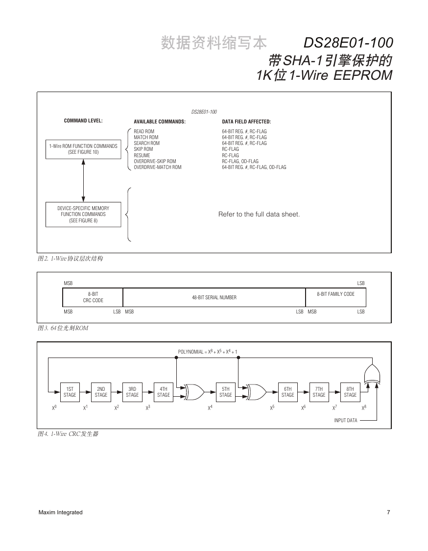
MSB
MSB
8-BIT
CRC CODE
LSB
MSB
48-BIT SERIAL NUMBER
8-BIT FAMILY CODE
LSB
MSB
LSB
LSB
POLYNOMIAL = X8 + X5 + X4 + 1
1ST
STAGE
2ND
STAGE
3RD
STAGE
4TH
STAGE
5TH
STAGE
6TH
STAGE
7TH
STAGE
8TH
STAGE
X0
X1
X2
X3
X4
X5
X6
X7
X8
INPUT DATA
Maxim Integrated7DS28E01-100�
BIT #
7
TARGET ADDRESS (TA1)
T7
6
T6
5
T5
4
T4
3
T3
2
T2
(0)
1
T1
(0)
0
T0
(0)
TARGET ADDRESS (TA2)
T15
T14
T13
T12
T11
T10
T9
T8
ENDING ADDRESS WITH
DATA STATUS (E/S)
(READ ONLY)
AA
1
PF
1
1
E2
(1)
E1
(1)
E0
(1)
DS28E01-1008Maxim Integrated8�



 2023年江西萍乡中考道德与法治真题及答案.doc
 2012年重庆南川中考生物真题及答案.doc
 2013年江西师范大学地理学综合及文艺理论基础考研真题.doc
 2020年四川甘孜小升初语文真题及答案I卷.doc
 2020年注册岩土工程师专业基础考试真题及答案.doc
 2023-2024学年福建省厦门市九年级上学期数学月考试题及答案.doc
 2021-2022学年辽宁省沈阳市大东区九年级上学期语文期末试题及答案.doc
 2022-2023学年北京东城区初三第一学期物理期末试卷及答案.doc
 2018上半年江西教师资格初中地理学科知识与教学能力真题及答案.doc
 2012年河北国家公务员申论考试真题及答案-省级.doc
 2020-2021学年江苏省扬州市江都区邵樊片九年级上学期数学第一次质量检测试题及答案.doc
 2022下半年黑龙江教师资格证中学综合素质真题及答案.doc