JEDEC
PUBLICATION
Failure Mechanisms and Models for
Semiconductor Devices
JEP122H
(Revision of JEP122G, October 2011)
SEPTEMBER 2016
JEDEC SOLID STATE TECHNOLOGY ASSOCIATION
�
NOTICE
JEDEC standards and publications contain material that has been prepared, reviewed, and
approved through the JEDEC Board of Directors level and subsequently reviewed and approved
by the JEDEC legal counsel.
JEDEC standards and publications are designed to serve the public interest through eliminating
misunderstandings between manufacturers and purchasers, facilitating interchangeability and
improvement of products, and assisting the purchaser in selecting and obtaining with minimum
delay the proper product for use by those other than JEDEC members, whether the standard is to
be used either domestically or internationally.
JEDEC standards and publications are adopted without regard to whether or not their adoption
may involve patents or articles, materials, or processes. By such action JEDEC does not assume
any liability to any patent owner, nor does it assume any obligation whatever to parties adopting
the JEDEC standards or publications.
The information included in JEDEC standards and publications represents a sound approach to
product specification and application, principally from the solid state device manufacturer
viewpoint. Within the JEDEC organization there are procedures whereby a JEDEC standard or
publication may be further processed and ultimately become an ANSI standard.
No claims to be in conformance with this standard may be made unless all requirements stated in
the standard are met.
Inquiries, comments, and suggestions relative to the content of this JEDEC standard or
publication should be addressed to JEDEC at the address below, or refer to www.jedec.org under
Standards and Documents for alternative contact information.
©JEDEC Solid State Technology Association 2016
Published by
3103 North 10th Street
Suite 240 South
Arlington, VA 22201-2107
This document may be downloaded free of charge; however JEDEC retains the
copyright on this material. By downloading this file the individual agrees not to
charge for or resell the resulting material.
PRICE: Contact JEDEC
Printed in the U.S.A.
All rights reserved
�
PLEASE!
DON’T VIOLATE
THE
LAW!
This document is copyrighted by JEDEC and may not be
reproduced without permission.
For information, contact:
JEDEC Solid State Technology Association
3103 North 10th Street
Suite 240 South
Arlington, VA 22201-2107
or refer to www.jedec.org under Standards-Documents/Copyright Information.
�
�
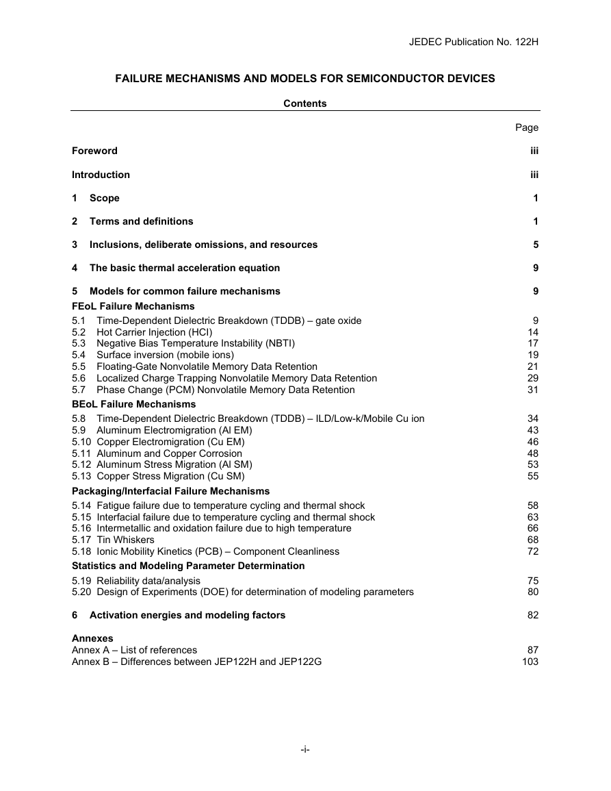
FAILURE MECHANISMS AND MODELS FOR SEMICONDUCTOR DEVICES
JEDEC Publication No. 122H
Contents
Inclusions, deliberate omissions, and resources
Foreword
Introduction
1 Scope
2 Terms and definitions
3
4 The basic thermal acceleration equation
5 Models for common failure mechanisms
FEoL Failure Mechanisms
5.1 Time-Dependent Dielectric Breakdown (TDDB) – gate oxide
5.2 Hot Carrier Injection (HCI)
5.3 Negative Bias Temperature Instability (NBTI)
5.4 Surface inversion (mobile ions)
5.5 Floating-Gate Nonvolatile Memory Data Retention
5.6 Localized Charge Trapping Nonvolatile Memory Data Retention
5.7 Phase Change (PCM) Nonvolatile Memory Data Retention
BEoL Failure Mechanisms
5.8 Time-Dependent Dielectric Breakdown (TDDB) – ILD/Low-k/Mobile Cu ion
5.9 Aluminum Electromigration (Al EM)
5.10 Copper Electromigration (Cu EM)
5.11 Aluminum and Copper Corrosion
5.12 Aluminum Stress Migration (Al SM)
5.13 Copper Stress Migration (Cu SM)
Packaging/Interfacial Failure Mechanisms
5.14 Fatigue failure due to temperature cycling and thermal shock
5.15 Interfacial failure due to temperature cycling and thermal shock
5.16 Intermetallic and oxidation failure due to high temperature
5.17 Tin Whiskers
5.18 Ionic Mobility Kinetics (PCB) – Component Cleanliness
Statistics and Modeling Parameter Determination
5.19 Reliability data/analysis
5.20 Design of Experiments (DOE) for determination of modeling parameters
6 Activation energies and modeling factors
Annexes
Annex A – List of references
Annex B – Differences between JEP122H and JEP122G
-i-
Page
iii
iii
1
1
5
9
9
9
14
17
19
21
29
31
34
43
46
48
53
55
58
63
66
68
72
75
80
82
87
103
�
JEDEC Publication No. 122H
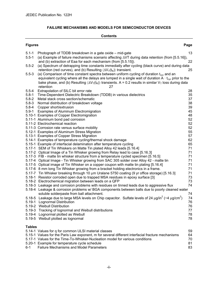
FAILURE MECHANISMS AND MODELS FOR SEMICONDUCTOR DEVICES
Contents
25
Figures
5.1-1 Photograph of TDDB breakdown in a gate oxide – mid-gate
5.5-1 (a) Example of failure mechanisms scenario affecting ΔVT during data retention (from [5.5.16]),
5.5-2 (a) Spectrum of detrapping time constants immediatly after cycling (black curve) and during data
and (b) extraction of Eaa for each mechanism (from [5.5.15]).
Page
13
22
retention (red curves), and (b) Resulting ΔVT(tR) transient.
5.5-3 (a) Comparison of time constant spectra between uniform cycling of duration tcyc and an
equivalent cycling where all the delays are lumped in a single wait of duration A · tcyc prior to the
bake phase, and (b) Resulting ΔVT(tR) transients. A = 0.2 results in similar VT loss during data
retention
27
5.5-4 Extrapolation of SILC bit error rate
5.8-1 Time-Dependent Dielectric Breakdown (TDDB) in various dielectrics
5.8-2 Metal stack cross section/schematic
5.8-3 Normal distribution of breakdown voltage
5.8-4 Copper short/extrusion
5.9-1 Examples of Aluminum Electromigration
5.10-1 Examples of Copper Electromigration
5.11-1 Aluminum bond pad corrosion
5.11-2 Electrochemical reaction
5.11-3 Corrosion rate versus surface mobility
5.12-1 Examples of Aluminum Stress Migration
5.13-1 Examples of Copper Stress Migration
5.14-1 Examples of temperature cycling/thermal shock damage
5.15-1 Example of interfacial delamination after temperature cycling
5.17-1 SEM of Tin Whiskers on Matte Tin plated Alloy 42 leads [5.16.4]
5.17-2 Optical Image of a Tin Whisker growing from Relay lead to case [5.16.3]
5.17-3 FIB - matte tin whisker structure from a temperature cycled specimen [5.16.5]
5.17-4 Optical Image - Tin Whisker growing from SAC 305 solder over Alloy 42 - matte tin
5.17-5 Optical image of Tin Whisker on a copper coupon with matte tin plating [5.16.4]
5.17-6 8 mm long Tin Whisker growing from a bracket holding electronics in a frame.
5.17-7 Tin Whisker breaking through 10 μm Uralane 5750 coating (9 yr office storage) [5.16.3]
5.18-1 Resistor corroded open due to trapped MSA residues in epoxy surface [3]
5.18-2 Electrochemical migration between leads on a QFP
5.18-3 Leakage and corrosion problems with residues on tinned leads due to aggressive flux
5.18-4 Leakage & corrosion problems w/ BGA components between balls due to poorly cleaned water
28
35
37
38
39
45
48
52
52
52
55
57
62
65
71
71
71
71
71
71
71
73
73
74
soluble solderpaste from ball attachment.
5.18-5 Leakage due to large MSA levels on Chip capacitor. Sulfate levels of 24 μg/in2 (~4 μg/cm2)
5.19-1 Lognormal Distribution
5.19-2 Weibull Distribution
5.19-3 Tracking of lognormal and Weibull distributions
5.19-4 Lognormal plotted as Weibull
5.19-5 Weibull plotted as lognormal
Tables
5.14-1 Values for q for common ULSI material classes
5.15-1 Values for the Paris Law exponent, m for several different interfacial fracture mechanisms
5.17-1 Values for the Time-To-Whisker-Nucleation model for various conditions
5.20-1 Example for temperature cycle schedule
6-1 Failure Mechanisms and Model Parameters
74
74
76
76
77
78
78
59
64
70
81
83
-ii-
�
JEDEC Publication No. 122H
FAILURE MECHANISMS AND MODELS FOR SEMICONDUCTOR DEVICES
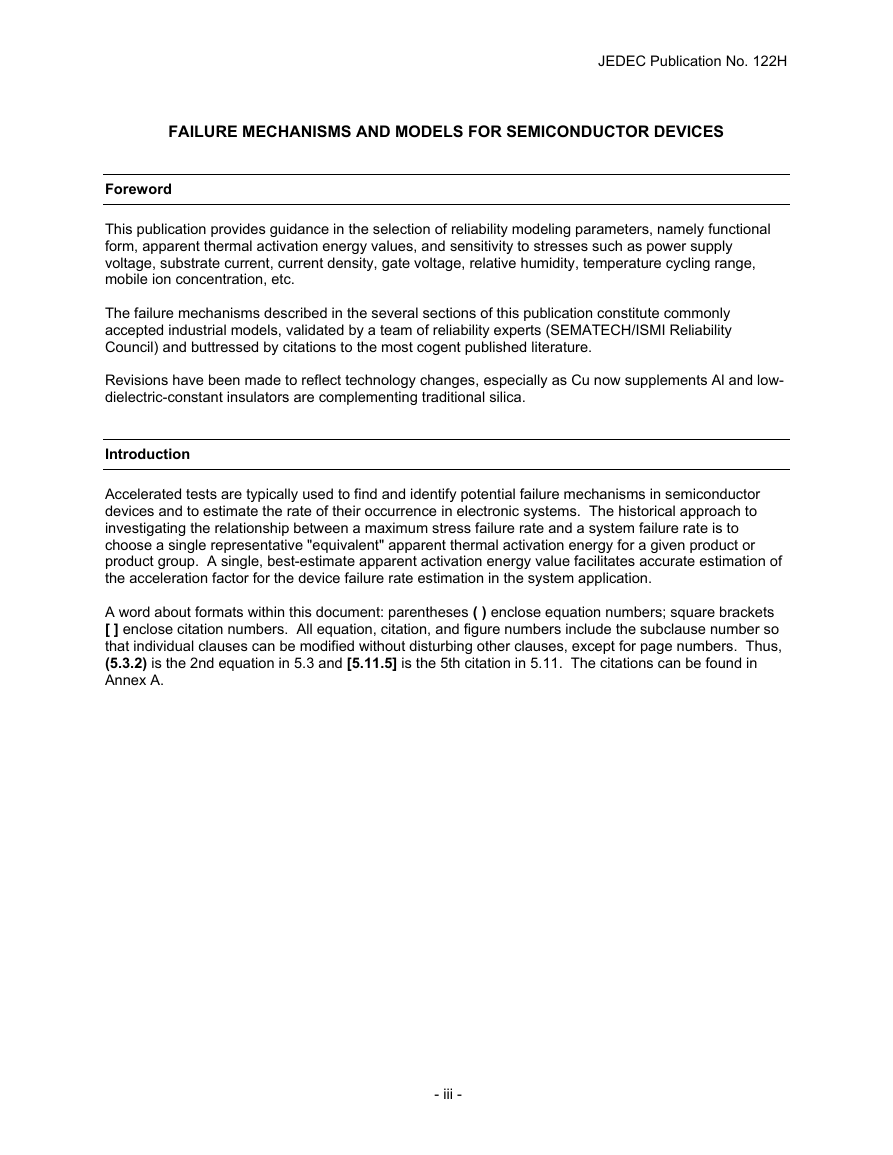
Foreword
This publication provides guidance in the selection of reliability modeling parameters, namely functional
form, apparent thermal activation energy values, and sensitivity to stresses such as power supply
voltage, substrate current, current density, gate voltage, relative humidity, temperature cycling range,
mobile ion concentration, etc.
The failure mechanisms described in the several sections of this publication constitute commonly
accepted industrial models, validated by a team of reliability experts (SEMATECH/ISMI Reliability
Council) and buttressed by citations to the most cogent published literature.
Revisions have been made to reflect technology changes, especially as Cu now supplements Al and low-
dielectric-constant insulators are complementing traditional silica.
Introduction
Accelerated tests are typically used to find and identify potential failure mechanisms in semiconductor
devices and to estimate the rate of their occurrence in electronic systems. The historical approach to
investigating the relationship between a maximum stress failure rate and a system failure rate is to
choose a single representative "equivalent" apparent thermal activation energy for a given product or
product group. A single, best-estimate apparent activation energy value facilitates accurate estimation of
the acceleration factor for the device failure rate estimation in the system application.
A word about formats within this document: parentheses ( ) enclose equation numbers; square brackets
[ ] enclose citation numbers. All equation, citation, and figure numbers include the subclause number so
that individual clauses can be modified without disturbing other clauses, except for page numbers. Thus,
(5.3.2) is the 2nd equation in 5.3 and [5.11.5] is the 5th citation in 5.11. The citations can be found in
Annex A.
- iii -
�
JEDEC Publication No. 122H
-iv-
�



 2023年江西萍乡中考道德与法治真题及答案.doc
 2012年重庆南川中考生物真题及答案.doc
 2013年江西师范大学地理学综合及文艺理论基础考研真题.doc
 2020年四川甘孜小升初语文真题及答案I卷.doc
 2020年注册岩土工程师专业基础考试真题及答案.doc
 2023-2024学年福建省厦门市九年级上学期数学月考试题及答案.doc
 2021-2022学年辽宁省沈阳市大东区九年级上学期语文期末试题及答案.doc
 2022-2023学年北京东城区初三第一学期物理期末试卷及答案.doc
 2018上半年江西教师资格初中地理学科知识与教学能力真题及答案.doc
 2012年河北国家公务员申论考试真题及答案-省级.doc
 2020-2021学年江苏省扬州市江都区邵樊片九年级上学期数学第一次质量检测试题及答案.doc
 2022下半年黑龙江教师资格证中学综合素质真题及答案.doc