Zynq-7000 All Programmable SoC
Table of Contents
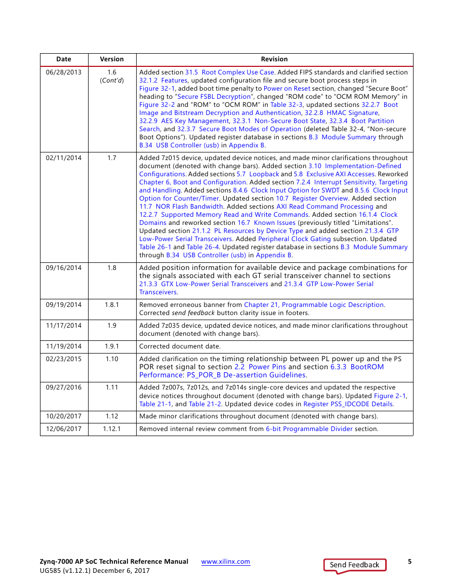
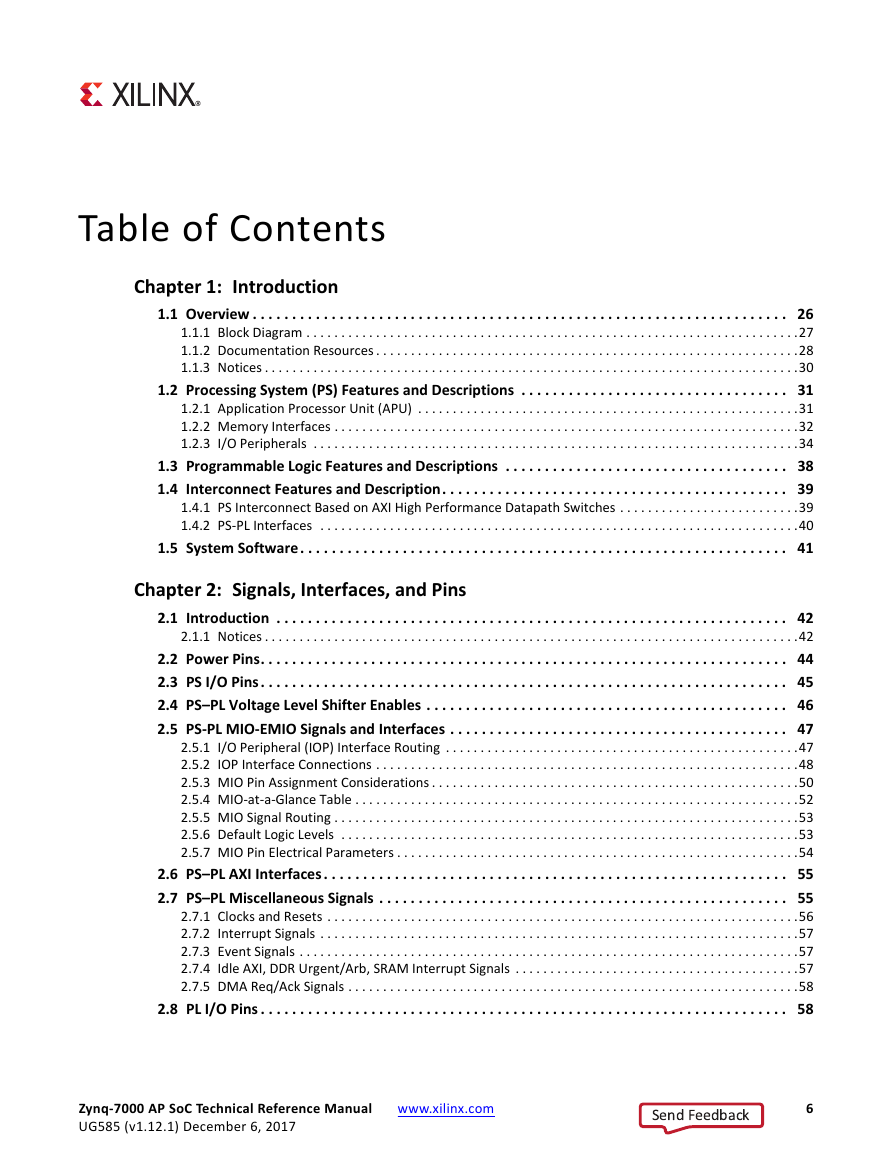
Ch. 1: Introduction
Overview
Block Diagram
Documentation Resources
Notices
Processing System (PS) Features and Descriptions
Application Processor Unit (APU)
Memory Interfaces
I/O Peripherals
Programmable Logic Features and Descriptions
Interconnect Features and Description
PS Interconnect Based on AXI High Performance Datapath Switches
PS-PL Interfaces
System Software
Ch. 2: Signals, Interfaces, and Pins
Introduction
Notices
Power Pins
PS I/O Pins
PS–PL Voltage Level Shifter Enables
PS-PL MIO-EMIO Signals and Interfaces
I/O Peripheral (IOP) Interface Routing
IOP Interface Connections
MIO Pin Assignment Considerations
MIO-at-a-Glance Table
MIO Signal Routing
Default Logic Levels
MIO Pin Electrical Parameters
PS–PL AXI Interfaces
PS–PL Miscellaneous Signals
Clocks and Resets
Interrupt Signals
Event Signals
Idle AXI, DDR Urgent/Arb, SRAM Interrupt Signals
DMA Req/Ack Signals
PL I/O Pins
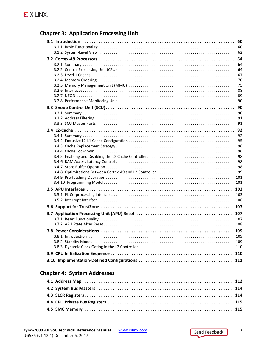
Ch. 3: Application Processing Unit
Introduction
Basic Functionality
System-Level View
Cortex-A9 Processors
Summary
Central Processing Unit (CPU)
Level 1 Caches
Memory Ordering
Memory Management Unit (MMU)
Interfaces
NEON
Performance Monitoring Unit
Snoop Control Unit (SCU)
Summary
Address Filtering
SCU Master Ports
L2-Cache
Summary
Exclusive L2-L1 Cache Configuration
Cache Replacement Strategy
Cache Lockdown
Enabling and Disabling the L2 Cache Controller
RAM Access Latency Control
Store Buffer Operation
Optimizations Between Cortex-A9 and L2 Controller
Pre-fetching Operation
Programming Model
APU Interfaces
PL Co-processing Interfaces
Interrupt Interface
Support for TrustZone
Application Processing Unit (APU) Reset
Reset Functionality
APU State After Reset
Power Considerations
Introduction
Standby Mode
Dynamic Clock Gating in the L2 Controller
CPU Initialization Sequence
Implementation-Defined Configurations
Ch. 4: System Addresses
Address Map
System Bus Masters
SLCR Registers
CPU Private Bus Registers
SMC Memory
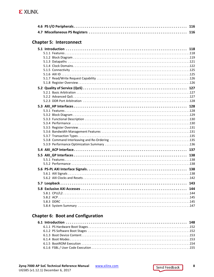
PS I/O Peripherals
Miscellaneous PS Registers
Ch. 5: Interconnect
Introduction
Features
Block Diagram
Datapaths
Clock Domains
Connectivity
AXI ID
Read/Write Request Capability
Register Overview
Quality of Service (QoS)
Basic Arbitration
Advanced QoS
DDR Port Arbitration
AXI_HP Interfaces
Features
Block Diagram
Functional Description
Performance
Register Overview
Bandwidth Management Features
Transaction Types
Command Interleaving and Re-Ordering
Performance Optimization Summary
AXI_ACP Interface
AXI_GP Interfaces
Features
Performance
PS-PL AXI Interface Signals
AXI Signals
AXI Clocks and Resets
Loopback
Exclusive AXI Accesses
CPU/L2
ACP
DDRC
System Summary
Ch. 6: Boot and Configuration
Introduction
PS Hardware Boot Stages
PS Software Boot Stages
Boot Device Content
Boot Modes
BootROM Execution
FSBL / User Code Execution
PL Boot Process
PL Configuration Paths
Device Configuration Interface
Starting Code on CPU 1
Development Environment
Device Start-up
Introduction
Power Requirements
Clocks and PLLs
Reset Operations
Boot Mode Pin Settings
I/O Pin Connections for Boot Devices
BootROM Code
BootROM Flowchart
BootROM Header
BootROM Performance
Quad-SPI Boot
NAND Boot
NOR Boot
SD Card Boot
JTAG Boot
Reset, Boot, and Lockdown States
BootROM Header Search
MultiBoot
BootROM Error Codes
Post BootROM State
Registers Modified by the BootROM – Examples
Device Boot and PL Configuration
PL Control via PS Software
Boot Sequence Examples
PCAP Bridge to PL
PCAP Datapath Configurations
PL Control via User-JTAG
Reference Section
PL Configuration Considerations
Boot Time Reference
Register Overview
PS Version and Device Revision
Ch. 7: Interrupts
Environment
Private, Shared and Software Interrupts
Generic Interrupt Controller (GIC)
Resets and Clocks
Block Diagram
CPU Interrupt Signal Pass-through
Functional Description
Software Generated Interrupts (SGI)
CPU Private Peripheral Interrupts (PPI)
Shared Peripheral Interrupts (SPI)
Interrupt Sensitivity, Targeting and Handling
Wait for Interrupt Event Signal (WFI)
Register Overview
Write Protection Lock
Programming Model
Interrupt Prioritization
Interrupt Handling
ARM Programming Topics
Legacy Interrupts and Security Extensions
Ch. 8: Timers
Introduction
System Diagram
Notices
CPU Private Timers and Watchdog Timers
Clocking
Interrupt to PS Interrupt Controller
Resets
Register Overview
Global Timer (GT)
Clocking
Register Overview
System Watchdog Timer (SWDT)
Features
Block Diagram
Functional Description
Register Overview
Programming Model
Clock Input Option for SWDT
Reset Output Option for SWDT
Triple Timer Counters (TTC)
Features
Block Diagram
Functional Description
Register Overview
Programming Model
Clock Input Option for Counter/Timer
I/O Signals
Ch. 9: DMA Controller
Introduction
Features
System Viewpoint
Block Diagram
Notices
Functional Description
DMA Transfers on the AXI Interconnect
AXI Transaction Considerations
DMA Manager
Multi-channel Data FIFO (MFIFO)
Memory-to-Memory Transfers
PL Peripheral AXI Transactions
PL Peripheral Request Interface
PL Peripheral - Length Managed by PL Peripheral
PL Peripheral - Length Managed by DMAC
Events and Interrupts
Aborts
Security
IP Configuration Options
Programming Guide for DMA Controller
Startup
Execute a DMA Transfer
Interrupt Service Routine
Register Overview
Programming Guide for DMA Engine
Write Microcode to Program CCRx for AXI Transactions
Memory-to-Memory Transfers
PL Peripheral DMA Transfer Length Management
Restart Channel using an Event
Interrupting a Processor
Instruction Set Reference
Programming Restrictions
Updating Channel Control Registers During a DMA Cycle
System Functions
Clocks
Resets
Reset Configuration of Controller
I/O Interface
AXI Master Interface
Peripheral Request Interface
Ch. 10: DDR Memory Controller
Introduction
Features
Block Diagram
Notices
Interconnect
DDR Memory Types, Densities, and Data Widths
I/O Signals
AXI Memory Port Interface (DDRI)
Introduction
Block Diagram
AXI Feature Support and Limitations
TrustZone
DDR Core and Transaction Scheduler (DDRC)
Row/Bank/Column Address Mapping
DDRC Arbitration
Priority, Aging Counter and Urgent Signals
Page-Match
Aging Counter
Stage 1 – AXI Port Arbitration
Stage 2 – Read Versus Write
High Priority Read Ports
Stage 3 – Transaction State
Read Priority Management
Write Combine
Credit Mechanism
Controller PHY (DDRP)
Functional Programming Model
Clock Operating Frequencies
DDR IOB Impedance Calibration
DDR IOB Configuration
DDR Controller Register Programming
DRAM Reset and Initialization
DDR Initialization Sequence
DRAM Input Impedance (ODT) Calibration
DRAM Output Impedance (RON) Calibration
DRAM Training
Write Data Eye Adjustment
Alternatives to Automatic DRAM Training
DRAM Write Latency Restriction
Register Overview
DDRI
DDRC
DDRP
Error Correction Code (ECC)
ECC Initialization
ECC Error Behavior
Data Mask During ECC Mode
ECC Programming Model
Operational Programming Model
Operating Modes
Changing Clock Frequencies
Power Down
Deep Power Down
Self Refresh
DDR Power Reduction
Ch. 11: Static Memory Controller
Introduction
Features
Block Diagram
Notices
Functional Operation
Boot Device
Clocks
Resets
ECC Support
Interrupts
PL353 Functionality
Address Map
I/O Signals
Wiring Diagrams
Register Overview
Programming Model
NOR Flash Bandwidth
Ch. 12: Quad-SPI Flash Controller
Introduction
Features
System Viewpoint
Block Diagram
Notices
Functional Description
Operational Modes
I/O Mode
I/O Mode Transmit Registers (TXD)
I/O Mode Considerations
Linear Addressing Mode
Unsupported Devices
Supported Memory Read and Write Commands
Programming Guide
Configuration
Linear Addressing Mode
Configure I/O Mode
I/O Mode Interrupts
Rx/Tx FIFO Response to I/O Command Sequences
Register Overview
System Functions
Clocks
Resets
I/O Interface
Wiring Connections
MIO Programming
MIO Signals
Ch. 13: SD/SDIO Controller
Introduction
Key Features
System Viewpoint
Functional Description
AHB Interface and Interrupt Controller
SD/SDIO Host Controller
Data FIFO
Command and Control Logic
Bus Monitor
Stream Write and Read
Clocks
Soft Resets
FIFO Overrun and Underrun Conditions
Programming Model
Data Transfer Protocol Overview
Data Transfers Without DMA
Using DMA
Using ADMA
Abort Transaction
External Interface Usage Example
Supported Configurations
Bus Voltage Translation
SDIO Controller Media Interface Signals
SDIO EMIO Considerations
Ch. 14: General Purpose I/O (GPIO)
Introduction
Features
Block Diagram
Notices
Functional Description
GPIO Control of Device Pins
EMIO Signals
Bank0, Bits[8:7] are Outputs
Interrupt Function
Programming Guide
Start-up Sequence
GPIO Pin Configurations
Writing Data to GPIO Output Pins
Reading Data from GPIO Input Pins
GPIO as Wake-up Event
Register Overview
System Functions
Clocks
Resets
Interrupts
I/O Interface
MIO Programming
Ch. 15: USB Host, Device, and OTG Controller
Introduction
Features
Operating Modes
Hardware System Viewpoint
Controller Block Diagram
Configuration, Control and Status
Data Structures
Implementation Summary
Documentation
Notices
Chapter Overview
Functional Description
Controller Flow Diagram
DMA Engine
Protocol Engine
Port Controller
ULPI Link Wrapper
General Purpose Timers
Programming Overview and Reference
Hardware/Software System
Operational Mode Control
Power Management
Register Overview
Interrupt and Status Bits Overview
OTG Status/Interrupt and Control Register
Device Mode Control
Controller State
USB Bus Reset Response
Device Endpoint Data Structures
Link-list Endpoint Descriptors
Manage Endpoints
Endpoint Registers
Endpoint Initialization
Device Endpoint Packet Operational Model
Prime Transmit Endpoints
Prime Receive Endpoints
Interrupt and Bulk Endpoint Operational Model
Isochronous Endpoint Operational Model
Control Endpoint Operational Model
Device Endpoint Descriptor Reference
Endpoint Queue Head Descriptor (dQH)
Endpoint Transfer Descriptor (dTD)
Endpoint Transfer Overlay Area
Programming Guide for Device Controller
Software Model
USB Reset
Register Controlled Reset
Programming Guide for Device Endpoint Data Structures
Device Controller Initialization Overview
Manage Transfer Descriptors
Manage Transfers with Transfer Descriptors
Service Device Mode Interrupts
Host Mode Data Structures
Host Controller Transfer Schedule Structures
Periodic Schedule
Asynchronous Schedule
EHCI Implementation
Overview
Embedded Transaction Translator
EHCI Functional Changes for the TT
Port Reset Timer Enhancement
Port Speed Detection Mechanism
FS/LS Data Structures
Operational Model of the TT
Port Test Mode
Host Data Structures Reference
Descriptor Usage
Transfer Descriptor Type (TYP) Field
Isochronous (High Speed) Transfer Descriptor (iTD)
Split Transaction Isochronous Transfer Descriptor (siTD)
Queue Element Transfer Descriptor (qTD)
Queue Head (QH)
Transfer Overlay Area
Periodic Frame Span Traversal Node (FSTN)
Programming Guide for Host Controller
Controller Reset
Run/Stop
OTG Description and Reference
Hardware Assistance Features
OTG Interrupt and Control Bits
System Functions
Clocks
Reset Types
System Interrupt
APB Slave Interface
AHB Master Interface
I/O Interfaces
Wiring Connections
MIO-EMIO Programming
MIO-EMIO Signals
Ch. 16: Gigabit Ethernet Controller
Introduction
Block Diagram
Features
System Viewpoint
Clock Domains
Notices
Application Notes
Functional Description and Programming Model
MAC Transmitter
MAC Receiver
MAC Filtering
Wake-on-LAN Support
DMA Block
Checksum Offloading
IEEE 1588 Time Stamp Unit
MAC 802.3 Pause Frame Support
Programming Guide
Initialize the Controller
Configure the Controller
I/O Configuration
Configure the PHY
Configure the Buffer Descriptors
Configure Interrupts
Enable the Controller
Transmitting Frames
Receiving Frames
Debug Guide
IEEE 1588 Time Stamping
Overview
Controller Initialization
Best Master Clock Algorithm (BMCA)
PTP Packet Handling at the Master
PTP Packet Handling at the Slave
Register Overview
Control Registers
Status and Statistics Registers
Signals and I/O Connections
MIO–EMIO Interface Routing
Precision Time Protocol
Programmable Logic (PL) Implementations
RGMII Interface via MIO
GMII/MII Interface via EMIO
MDIO Interface Signals via MIO and EMIO
MIO Pin Considerations
Known Issues
Ch. 17: SPI Controller
Introduction
Features
System Viewpoint
Block Diagram
Notices
Functional Description
Master Mode
Multi-Master Capability
Slave Mode
FIFOs
FIFO Interrupts
Interrupt Register Bits, Logic Flow
SPI-to-SPI Connection
Programming Guide
Start-up Sequence
Controller Configuration
Master Mode Data Transfer
Slave Mode Data Transfer
Interrupt Service Routine
Register Overview
System Functions
Resets
Clocks
I/O Interfaces
Protocol
Back-to-Back Transfers
MIO/EMIO Routing
Wiring Connections
MIO/EMIO Signal Tables
Ch. 18: CAN Controller
Introduction
Features
System Viewpoint
Block Diagram
Notices
Functional Description
Controller Modes
Message Format
Message Buffering
Interrupts
Rx Message Filtering
Protocol Engine
CAN0-to-CAN1 Connection
Programming Guide
Overview
Configuration Mode State
Start-up Controller
Change Operating Mode
Write Messages to TxFIFO
Write Messages to TxHPB
Read Messages from RxFIFO
Register Overview
System Functions
Clocks
Resets
I/O Interface
MIO Programming
MIO-EMIO Signals
Ch. 19: UART Controller
Introduction
Features
System Viewpoint
Notices
Functional Description
Block Diagram
Control Logic
Baud Rate Generator
Transmit FIFO
Transmitter Data Stream
Receiver FIFO
Receiver Data Capture
I/O Mode Switch
UART0-to-UART1 Connection
Status and Interrupts
Modem Control
Programming Guide
Start-up Sequence
Configure Controller Functions
Transmit Data
Receive Data
RxFIFO Trigger Level Interrupt
Register Overview
System Functions
Clocks
Resets
I/O Interface
MIO Programming
MIO – EMIO Signals
Ch. 20: I2C Controller
Introduction
Features
System Block Diagram
Notices
Functional Description
Block Diagram
Master Mode
Slave Monitor Mode
Slave Mode
I2C Speed
Multi-Master Operation
I2C0-to-I2C1 Connection
Status and Interrupts
Programmer’s Guide
Start-up Sequence
Controller Configuration
Configure Interrupts
Data Transfers
Register Overview
System Functions
Clocks
Reset Controller
I/O Interface
Pin Programming
MIO-EMIO Interfaces
Ch. 21: Programmable Logic Description
Introduction
Features
PL Resources by Device Type
Notices
PL Components
CLBs, Slices, and LUTs
Clock Management
Block RAM
Digital Signal Processing — DSP Slice
Input/Output
PS-PL Interfaces
SelectIO
GTX Low-Power Serial Transceivers
GTP Low-Power Serial Transceivers
Integrated I/O Block for PCIe
Configuration
Ch. 22: Programmable Logic Design Guide
Introduction
Programmable Logic for Software Offload
Benefits of Using PL to Implement Software Algorithms
Designing PL Accelerators
PL Acceleration Limits
Power Offload
Real Time Offload
Reconfigurable Computing
PL and Memory System Performance Overview
Theoretical Bandwidth
DDR Efficiency
OCM Efficiency
Interconnect Throughput Bottlenecks
Choosing a Programmable Logic Interface
PL Interface Comparison Summary
Cortex-A9 CPU via General Purpose Masters
PS DMA Controller (DMAC) via General Purpose Masters
PL DMA via AXI High-Performance (HP) Interface
PL DMA via AXI ACP
PL DMA via General Purpose AXI Slave (GP)
Ch. 23: Programmable Logic Test and Debug
Introduction
Features
Block Diagram
System Viewpoint
Functional Description
Basic Operation
Packet Generation
Packet Format
Signals
General-Purpose Debug Signals
Trigger Signals
Trace Signals
Register Overview
Programming Model
FTM Security
Ch. 24: Power Management
Introduction
Features
System Design Considerations
Device Technology Choice
PL Power-down Control
APU Maximum Frequency
DDR Memory Clock Frequency
DDR Memory Controller Modes and Configurations
Boot Interface Options
PS Clock Gating
Programming Guides
System Modules
Peripherals
I/O Buffers
Sleep Mode
Setup Wake-up Events
Programming Guide
Register Overview
Ch. 25: Clocks
Introduction
System Block Diagram
Clock Generation
System Viewpoint
Power Management
CPU Clock
System-wide Clock Frequency Examples
Clock Generator Design
DDR Clocks
IOP Module Clocks
USB Clocks
Ethernet Clocks
SDIO, SMC, SPI, Quad-SPI and UART Clocks
CAN Clocks
GPIO and I2C Clocks
PL Clocks
Clock Throttle
Clock Throttle Programming
Trace Port Clock
Register Overview
Programming Model
Branch Clock Generator
DDR Clocks
Digitally Controlled Impedance (DCI) Clock
PLLs
Ch. 26: Reset System
Introduction
Features
Block Diagram
Reset Hierarchy
Boot Flow
Reset Sources
Power-on Reset (PS_POR_B)
External System Reset (PS_SRST_B)
System Software Reset
Watchdog Timer Resets
Secure Violation Lock Down
Debug Resets
Reset Effects
Peripherals
PL Resets
PL General Purpose User Resets
Register Overview
Persistent Registers
System Reset Control
Peripheral Reset Control
Ch. 27: JTAG and DAP Subsystem
Introduction
Block Diagram
Features
Functional Description
I/O Signals
Programming Model
Use Case I: Software Debug with Trace Port Enabled
Use Case II: PS and PL Debug with Trace Port Enabled
ARM DAP Controller
Trace Port Interface Unit (TPIU)
Xilinx TAP Controller
Ch. 28: System Test and Debug
Introduction
Features
Notices
Functional Description
Debug Access Port (DAP)
Embedded Cross Trigger (ECT)
Program Trace Macrocell (PTM)
Instrumentation Trace Macrocell (ITM)
Funnel
Embedded Trace Buffer (ETB)
Trace Packet Output (TPIU)
I/O Signals
Register Overview
Memory Map
Functionality
Programming Model
Authentication Requirements
Ch. 29: On-Chip Memory (OCM)
Introduction
Block Diagram
Features
System Viewpoint
Functional Description
Overview
Optimal Transfer Alignment
Clocking
Arbitration Scheme
Address Mapping
Interrupts
Register Overview
Programming Model
Changing Address Mapping
AXI Responses
Ch. 30: XADC Interface
Introduction
Features
System Viewpoint
PS-XADC Interface Block Diagram
Programming Guide
Functional Description
Interface Arbiter (PL-JTAG and PS-XADC)
Serial Communication Channel (PL-JTAG and PS-XADC)
Analog-to-Digital Converter (All)
Sensor Alarms (PS-XADC and DRP)
PS-XADC Interface Description
Serial Channel Clock Frequency
Command and Data Packets
Command Format
Read Data Format
Min/Max Voltage Thresholds
Critical Over-temperature Alarm
Programming Guide for the PS-XADC Interface
Read and Write to the FIFOs
Interrupts
Command Preparation
Register Overview
Programming Guide for the DRP Interface
Programming Guide for the PL-JTAG Interface
System Functions
Clocks
Resets
Ch. 31: PCI Express
Introduction
Block Diagram
Features
Endpoint Use Case
Root Complex Use Case
Ch. 32: Device Secure Boot
Introduction
Block Diagram
Features
Functional Description
Master Secure Boot
External Boot Devices
Secure Boot Image
eFUSE Settings
RSA Authentication
Boot Image and Bitstream Encryption
Boot Image and Bitstream Decryption and Authentication
HMAC Signature
AES Key Management
Secure Boot Features
Non-Secure Boot State
Secure Boot State
Security Lockdown
Boot Partition Search
JTAG and Debug Considerations
Readback
Secure Boot Modes of Operation
Programming Considerations
Appx. A: Additional Resources
Xilinx Resources
Solution Centers
References
Zynq-7000 AP SoC Documents
PL Documents – Device and Boards
Additional Zynq-7000 AP SoC Documents
Software Programming Documents
git Information
Design Tool Resources
Xilinx Problem Solvers
Third-Party IP and Standards Documents
Appx. B: Register Details
Overview
Acronyms
Module Summary
AXI_HP Interface (AFI) (axi_hp)
CAN Controller (can)
DDR Memory Controller (ddrc)
CoreSight Cross Trigger Interface (cti)
Performance Monitor Unit (cortexa9_pmu)
CoreSight Program Trace Macrocell (ptm)
Debug Access Port (dap)
CoreSight Embedded Trace Buffer (etb)
PL Fabric Trace Monitor (ftm)
CoreSight Trace Funnel (funnel)
CoreSight Intstrumentation Trace Macrocell (itm)
CoreSight Trace Packet Output (tpiu)
Device Configuration Interface (devcfg)
DMA Controller (dmac)
Gigabit Ethernet Controller (GEM)
General Purpose I/O (gpio)
Interconnect QoS (qos301)
NIC301 Address Region Control (nic301_addr_region_ctrl_registers)
I2C Controller (IIC)
L2 Cache (L2Cpl310)
Application Processing Unit (mpcore)
On-Chip Memory (ocm)
Quad-SPI Flash Controller (qspi)
SD Controller (sdio)
System Level Control Registers (slcr)
Static Memory Controller (pl353)
SPI Controller (SPI)
System Watchdog Timer (swdt)
Triple Timer Counter (ttc)
UART Controller (UART)
USB Controller (usb)


 2023年江西萍乡中考道德与法治真题及答案.doc
 2012年重庆南川中考生物真题及答案.doc
 2013年江西师范大学地理学综合及文艺理论基础考研真题.doc
 2020年四川甘孜小升初语文真题及答案I卷.doc
 2020年注册岩土工程师专业基础考试真题及答案.doc
 2023-2024学年福建省厦门市九年级上学期数学月考试题及答案.doc
 2021-2022学年辽宁省沈阳市大东区九年级上学期语文期末试题及答案.doc
 2022-2023学年北京东城区初三第一学期物理期末试卷及答案.doc
 2018上半年江西教师资格初中地理学科知识与教学能力真题及答案.doc
 2012年河北国家公务员申论考试真题及答案-省级.doc
 2020-2021学年江苏省扬州市江都区邵樊片九年级上学期数学第一次质量检测试题及答案.doc
 2022下半年黑龙江教师资格证中学综合素质真题及答案.doc