1
�
3rd Order PLL Design
fR
Kf
Kv
fO
C2
R1
C1
1
N
Fig. 1: 3rd-Order PLL with Current-Mode Phase-Detector
useful functions and identities
Units
Constants
_______________________________________
Table of Contents
I.
Introduction
II.
Inputs
III.
Design Procedure
IV.
Optimal Phase Margin for Minimum Settling
V.
Synthesis of Loop Filter Components
VI.
Integrated Loop Filter
VII. Modified Loop Filter
PLL Design Function
VIII.
IX.
Copyright and Trademark Notice
2
S
�
_______________________________________
Introduction
The charge-pump-based third order PLL is the most popular PLL architecture today. This report discusses
the design and analysis and the loop dynamics of 3rd order PLLs. This includes phase margin sizing to minimize the
settling time of the PLL, and a anaylsis of a modified loop filter. There are other PLL topologies, such as those which
boost the current charge pump current initially for faster settling, these will be discussed in a later report. There are also
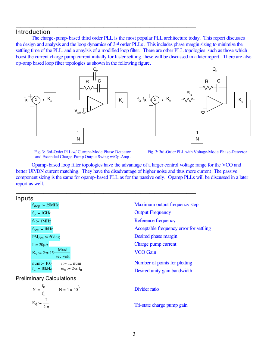
op-amp based loop filter topologies as shown in the following figure.
C2
R
C
C2
R
C
fR
Kf
Kv
fO
f R
Kf
RB
Kv
Vref
1
N
1
N
Fig. 3: 3rd-Order PLL w/ Current-Mode Phase Detector
and Extended Charge-Pump Output Swing w/Op-Amp.
Opamp-based loop filter topologies have the advantage of a larger control voltage range for the VCO and
Fig. 3: 3rd-Order PLL with Voltage-Mode Phase-Detector
better UP/DN current matching. They have the disadvantage of higher noise and thus more current. The passive
component sizing is the same for opamp-based PLL as for the passive only. Opamp PLLs will be discussed in a later
report as well.
_______________________________________
Inputs
:=
25MHz
1GHz
fstep
:=
fo
:=
fr
facc
PMdes
:=
I
Kv
1MHz
:=
1kHz
:=
20m A
2 p
:=
15
60deg
Mrad
sec volt
Maximum output frequency step
Output Frequency
Reference frequency
Acceptable frequency error for settling
Desired phase margin
Charge pump current
VCO Gain
:=
num 100
10kHz
fu
:=
:=
i
w u
1 num..
fu
:=
2 p
Preliminary Calculations
103
·=
N 1
:=
N
fo
fr
:=
Kf
I
2 p
Number of points for plotting
Desired unity gain bandwidth
Divider ratio
Tri-state charge pump gain
3
S
S
�
_______________________________________
3rd Order PLL Design Procedure
Without a loop filter PLLs are a type I system a single pole at DC from the VCO voltage to phase transfer
function. The loop filter accumulates the average charge from the charge pump to generate a fixed voltage to set the
frequency of the VCO. This accumulation gives the loop another pole at DC. Thus the loop starts with a phase of
-180 degrees. In order to insure stability and provide a smooth settling response the phase must be raised with a zero
in the loop to provide a desired phase margin at the unity gain frequency of the open loop transfer function. This zero is
introduced by adding a resistor in series with the main loop filter capacitor.
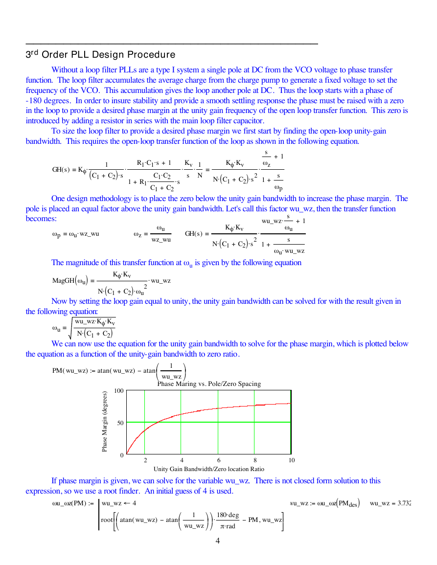
To size the loop filter to provide a desired phase margin we first start by finding the open-loop unity-gain
bandwidth. This requires the open-loop transfer function of the loop as shown in the following equation.
GH s( ) Kf
=
(
1
C1 C2+
) s
R1 C1
1+
s
C1 C2
C1 C2+
+
1 R1
Kv
s
1
N
=
Kf Kv
)
(
N C1 C2+
s2
s
s
w z
+
1
1+
s
w p
One design methodology is to place the zero below the unity gain bandwidth to increase the phase margin. The
pole is placed an equal factor above the unity gain bandwidth. Let's call this factor wu_wz, then the transfer function
becomes:
w p
w u wz_wu
wu_wz
GH s( )
1+
w z
=
=
=
w u
wz_wu
s
w u
s
Kf Kv
)
(
N C1 C2+
s2
+
1
w u wu_wz
u is given by the following equation
The magnitude of this transfer function at w
MagGH w u(
)
wu_wz
=
Kf Kv
)
(
N C1 C2+
2
w u
Now by setting the loop gain equal to unity, the unity gain bandwidth can be solved for with the result given in
the following equation:
Kv
wu_wz Kf
)
(
N C1 C2+
=
w u
We can now use the equation for the unity gain bandwidth to solve for the phase margin, which is plotted below
the equation as a function of the unity-gain bandwidth to zero ratio.
PM wu_wz
)
(
:=
atan wu_wz
)
(
atan
1
wu_wz
Phase Maring vs. Pole/Zero Spacing
)
s
e
e
r
g
e
d
(
n
i
g
r
a
M
e
s
a
h
P
100
50
0
2
4
6
8
10
Unity Gain Bandwidth/Zero location Ratio
If phase margin is given, we can solve for the variable wu_wz. There is not closed form solution to this
expression, so we use a root finder. An initial guess of 4 is used.
wu_wz
:=
(
w u_w z PMdes
)
wu_wz
=
3.732
w u_w z PM(
)
:=
wu_wz
4
root
atan wu_wz
)
(
atan
1
wu_wz
180 deg
rad
PM-
,
wu_wz
4
‹
Ł
ł
-
Ł
ł
p
Ø
Œ
º
ø
œ
ß
Ł
ł
-
�
_______________________________________
Optimal Phase Margin for Minimum Settling
Part of the design process involves entering a desired value of phase margin. The phase margin can effect the
performance of several parameters including phase noise, loop bandwidth, and settling time. It's effect on some
parameters is minor for typical values. Phase margin has it's biggest impact on settling time. Thus, settling time is used
to optimized phase margin. The variable w u_w z is easier to work with than phase margin, so it will be used. There is a
direct relationship between the two, which will be used to find the optimum phase margin.
ClosedLoop s( )
=
wu_wz
The transient response of this system is:
wu_wz
1+
N
s
w u
2
+
s
w u
s
w u
3
+
wu_wz
1+
s
w u
(
)
h w ut wu_wz
,
:=
fstep 1
+
2 e
wu_wz 1-
2
w ut
cosh
1
2
wu_wz
1+
wu_wz
3-
w ut
w ut
e
(
wu_wz
1-
)
wu_wz
3-
For the case where wu_wz=3 the response is
(
)
h w ut wu_wz
We can write a single expression for the transient response in both cases, when wu_wz is and isn't 3.
fstep 1
) e
w ut
w ut
1-
w ut
:=
(
+
2
,
1-
2
w ut
cosh
1
2
2 e
1+
3-
w ut
e-
(
2
) e
w ut
,
(
)
,
e
+
:=
3=
if b
1-
w ut
w ut
fstep 1
)
hlin w ut b,
3-
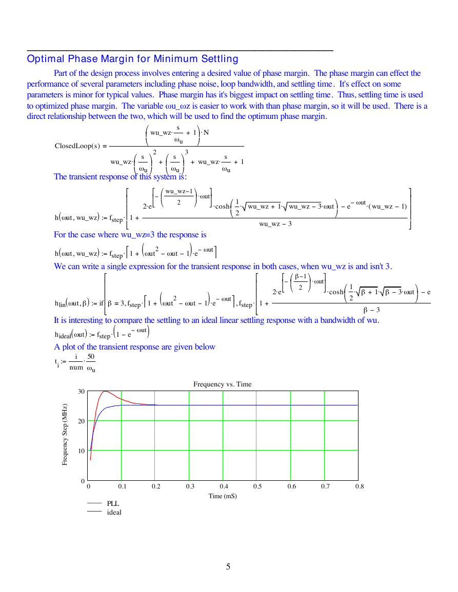
It is interesting to compare the settling to an ideal linear settling response with a bandwidth of wu.
hideal w ut
A plot of the transient response are given below
ti
(
fstep 1
fstep 1
w ut
:=
:=
+
(
)
i
num
50
w u
)
z
H
M
(
p
e
t
S
y
c
n
e
u
q
e
r
F
30
20
10
0
0
Frequency vs. Time
0.1
0.2
0.3
PLL
ideal
0.4
Time (mS)
0.5
0.6
0.7
0.8
5
Ł
ł
Ł
ł
Ł
ł
Ł
ł
-
Ø
Œ
º
ø
œ
ß
Ł
ł
-
-
Ø
Œ
Œ
Œ
º
ø
œ
œ
œ
ß
-
-
Ø
º
ø
ß
-
-
Ø
º
ø
ß
b
Ł
ł
-
Ø
Œ
º
ø
œ
ß
b
b
Ł
ł
b
Ø
Œ
Œ
Œ
º
Ø
Œ
Œ
Œ
º
-
-
�
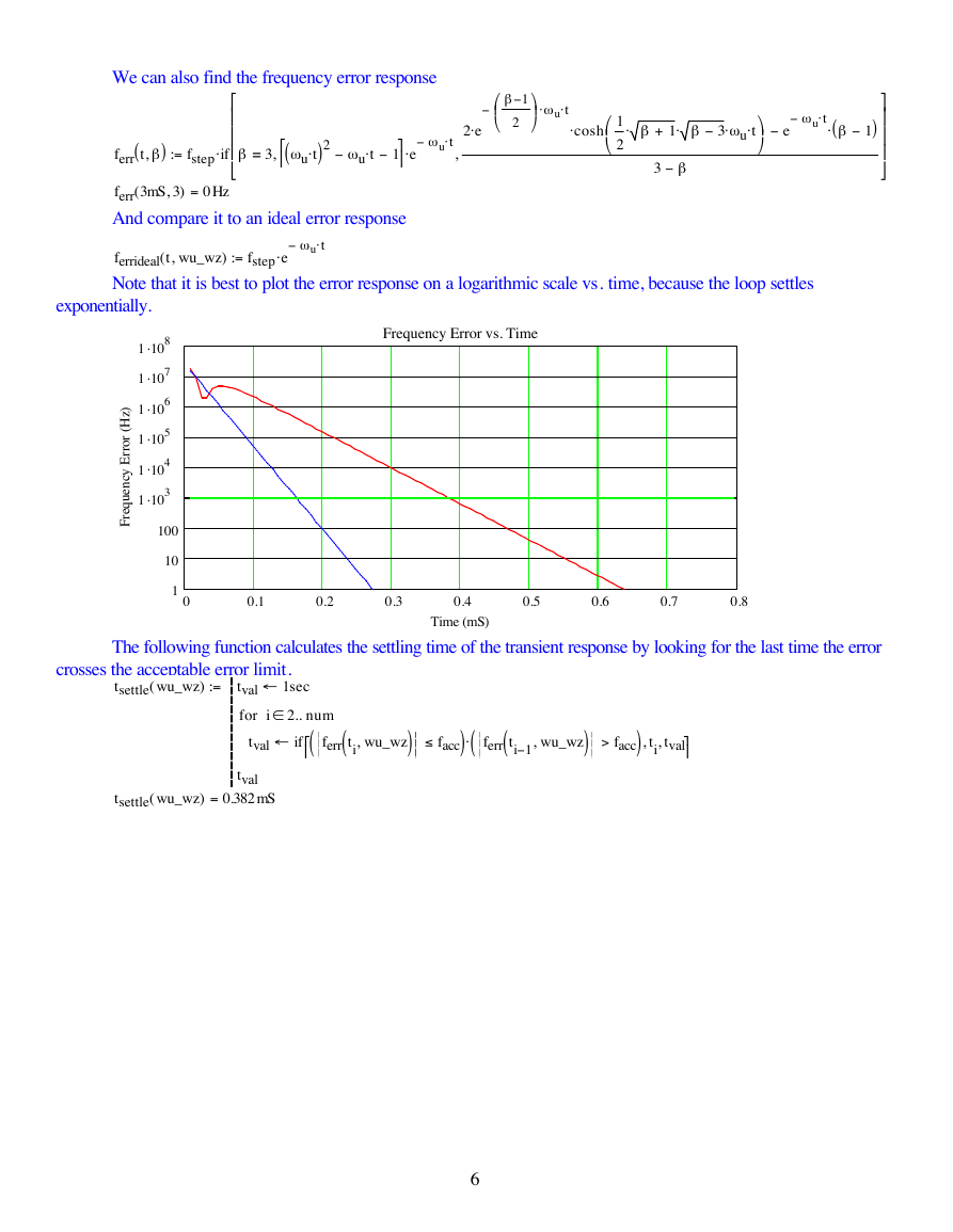
We can also find the frequency error response
(
)2
)
:=
,
3=
ferr t b,(
ferr 3mS 3,
(
)
And compare it to an ideal error response
fstep if b
=
w u t
w u t
0Hz
1-
ß e
2 e
w u
t
,
1-
2
w u
t
cosh
1
2
1+
3
3-
w u
t
w u
t
(
e
)
1-
,(
:=
ferrideal t wu_wz
)
Note that it is best to plot the error response on a logarithmic scale vs. time, because the loop settles
fstep e
w u
t
exponentially.
)
z
H
(
r
o
r
r
E
y
c
n
e
u
q
e
r
F
1 .108
1 .107
1 .106
1 .105
1 .104
1 .103
100
10
1
0
Frequency Error vs. Time
0.1
0.2
0.3
0.4
Time (mS)
0.5
0.6
0.7
0.8
The following function calculates the settling time of the transient response by looking for the last time the error
)
facc
(
(
ferr ti 1-
,
)
wu_wz
)
facc
>
,
,
ti
tval
6
crosses the acceptable error limit.
tsettle wu_wz
)
(
:=
tval
i
for
tval
1sec
2 num..
if
(
)
ferr ti wu_wz
,(
tsettle wu_wz
)
(
=
tval
0.382mS
-
Ø
º
ø
-
b
Ł
ł
-
b
b
Ł
ł
-
b
-
b
-
Ø
Œ
Œ
Œ
º
ø
œ
œ
œ
ß
-
‹
£
Ø
º
ø
ß
‹
˛
�
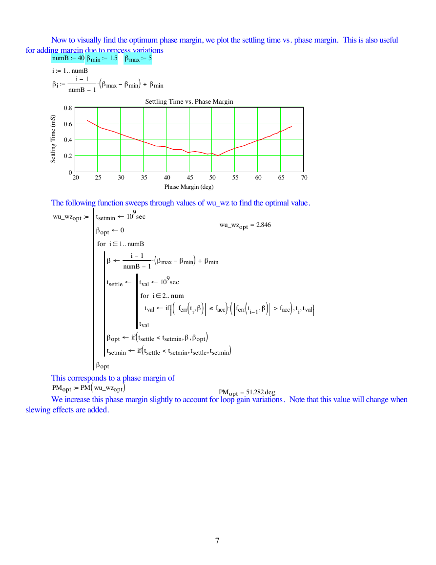
Now to visually find the optimum phase margin, we plot the settling time vs. phase margin. This is also useful
for adding margin due to process variations
b min
:=
1.5
b max
5:=
(
b max
)
b min
+
b min
Settling Time vs. Phase Margin
:=
numB 40
:=
..
1 numB
1-
:=
i
i
i
numB 1-
0.8
0.6
0.4
0.2
)
S
m
i
(
e
m
T
g
n
i
l
t
t
e
S
0
20
25
30
35
45
40
50
Phase Margin (deg)
55
60
65
70
The following function sweeps through values of wu_wz to find the optimal value.
wu_wzopt
109sec
:=
wu_wzopt
=
2.846
tsetmin
b opt
for
i
0
..
1 numB
1-
i
numB 1-
(
b max
)
b min
+
b min
tsettle
tval
i
for
tval
109sec
2 num..
(
if
b,(
ferr ti
)
)
facc
(
(
ferr ti 1-
)
b,
)
facc
>
,
,
ti
tval
tval
<
(
if tsettle
(
if tsettle
b opt
tsetmin
b opt
b,
tsetmin
<
tsetmin
)
b opt
,
tsettle
,
,
)
tsetmin
This corresponds to a phase margin of
PMopt
We increase this phase margin slightly to account for loop gain variations. Note that this value will change when
PM wu_wzopt
51.282deg
PMopt
:=
=
(
)
slewing effects are added.
7
b
-
‹
‹
b
-
‹
‹
£
Ø
º
ø
ß
‹
˛
‹
‹
‹
˛
�
_______________________________________
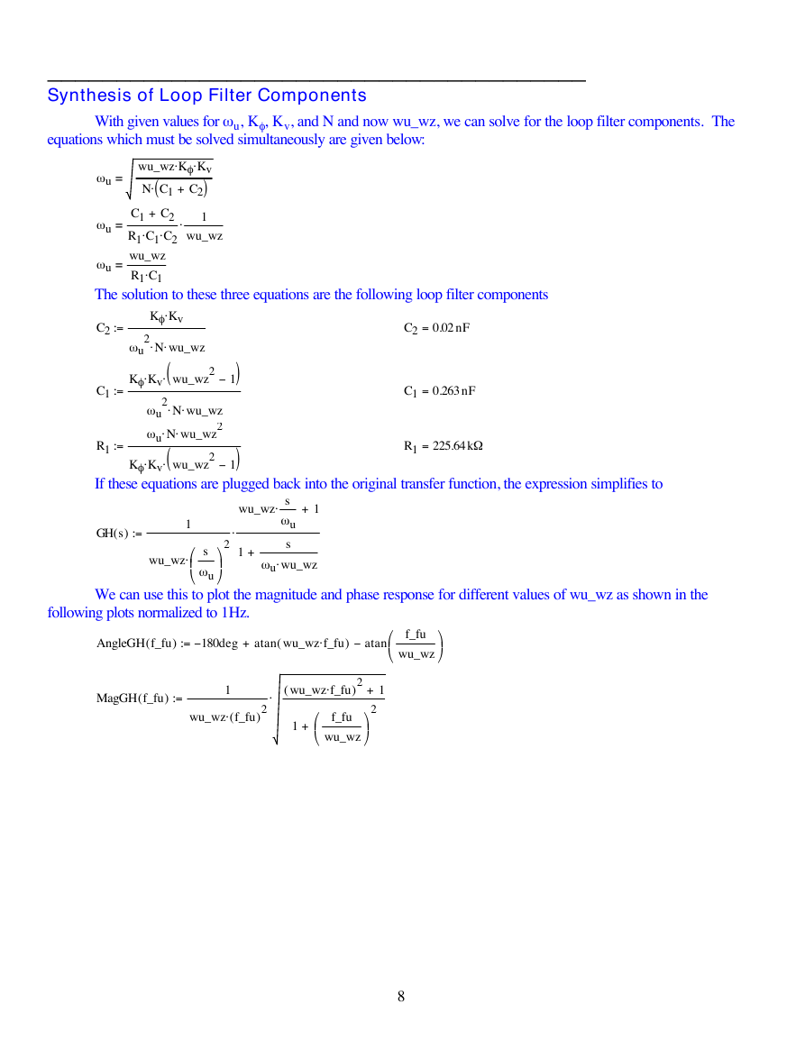
Synthesis of Loop Filter Components
With given values for w u, Kf , Kv, and N and now wu_wz, we can solve for the loop filter components. The
equations which must be solved simultaneously are given below:
w u
=
w u
=
Kv
wu_wz Kf
)
(
N C1 C2+
C1 C2+
1
R1 C1
C2
wu_wz
R1 C1
wu_wz
=
w u
The solution to these three equations are the following loop filter components
:=
C2
2
w u
Kf Kv
N
:=
C1
:=
R1
Kf Kv
2
w u
N
w u N
(
Kf Kv
wu_wz
wu_wz2
(
)
1-
wu_wz
wu_wz2
wu_wz2
)
1-
=
C2
0.02nF
=
C1
0.263nF
=
225.64kW
R1
If these equations are plugged back into the original transfer function, the expression simplifies to
wu_wz
1+
s
w u
s
GH s( )
:=
1
wu_wz
2
+
1
s
w u
w u wu_wz
We can use this to plot the magnitude and phase response for different values of wu_wz as shown in the
following plots normalized to 1Hz.
+
AngleGH f_fu
deg
180
:=
(
)
atan wu_wz f_fu
(
)
atan
f_fu
wu_wz
MagGH f_fu
(
)
:=
1
(
wu_wz f_fu
)2
wu_wz f_fu
(
)2
+
1
f_fu
wu_wz
1+
2
8
Ł
ł
-
Ł
ł
-
Ł
ł
�



 2023年江西萍乡中考道德与法治真题及答案.doc
 2012年重庆南川中考生物真题及答案.doc
 2013年江西师范大学地理学综合及文艺理论基础考研真题.doc
 2020年四川甘孜小升初语文真题及答案I卷.doc
 2020年注册岩土工程师专业基础考试真题及答案.doc
 2023-2024学年福建省厦门市九年级上学期数学月考试题及答案.doc
 2021-2022学年辽宁省沈阳市大东区九年级上学期语文期末试题及答案.doc
 2022-2023学年北京东城区初三第一学期物理期末试卷及答案.doc
 2018上半年江西教师资格初中地理学科知识与教学能力真题及答案.doc
 2012年河北国家公务员申论考试真题及答案-省级.doc
 2020-2021学年江苏省扬州市江都区邵樊片九年级上学期数学第一次质量检测试题及答案.doc
 2022下半年黑龙江教师资格证中学综合素质真题及答案.doc