Innovus User Guide
Product Version 15.20
November 2015
�
© 2014-2015 Cadence Design Systems, Inc. All rights reserved.
Printed in the United States of America.
Cadence Design Systems, Inc. (Cadence), 2655 Seely Ave., San Jose, CA 95134, USA.
Trademarks: Trademarks and service marks of Cadence Design Systems, Inc. (Cadence)
contained in this document are attributed to Cadence with the appropriate symbol. For queries
regarding Cadence's trademarks, contact the corporate legal department at the address shown
above or call 1-800-862-4522.
All other trademarks are the property of their respective holders.
Patents: Licensed under U.S. Patent Nos. 7,526,739; 8,032,857; 8,209,649; 8,266,560; 8,650,516
Restricted Print Permission: This publication is protected by copyright and any unauthorized use
of this publication may violate copyright, trademark, and other laws. Except as specified in this
permission statement, this publication may not be copied, reproduced, modified, published,
uploaded, posted, transmitted, or distributed in any way, without prior written permission from
Cadence. This statement grants you permission to print one (1) hard copy of this publication subject
to the following conditions:
1. The publication may be used solely for personal, informational, and noncommercial purposes;
2. The publication may not be modified in any way;
3. Any copy of the publication or portion thereof must include all original copyright, trademark,
and other proprietary notices and this permission statement; and
4. Cadence reserves the right to revoke this authorization at any time, and any such use shall be
discontinued immediately upon written notice from Cadence.
Disclaimer: Information in this publication is subject to change without notice and does not
represent a commitment on the part of Cadence. The information contained herein is the proprietary
and confidential information of Cadence or its licensors, and is supplied subject to, and may be
used only by Cadence's customer in accordance with, a written agreement between Cadence and
its customer. Except as may be explicitly set forth in such agreement, Cadence does not make, and
expressly disclaims, any representations or warranties as to the completeness, accuracy or
usefulness of the information contained in this document. Cadence does not warrant that use of
such information will not infringe any third party rights, nor does Cadence assume any liability for
damages or costs of any kind that may result from use of such information.
Restricted Rights: Use, duplication, or disclosure by the Government is subject to restrictions as
set forth in FAR52.227-14 and DFAR252.227-7013 et seq. or its successor.
�
�
Innovus User Guide
Table of Contents
Contents
About This Manual
Audience
How This Manual Is Organized
Conventions Used in This Manual
Related Documents
Additional Learning Resources
1
Product and Licensing Information
Overview
Innovus System Products and Product Options
Innovus
Virtuoso Digital Implementation
First Encounter
Product Options
Migration and Upgrade
Migration and Upgrade for Base Products
Migration and Upgrade for Product Options
Licensing Information
Licensing Terminology
Dynamic Licensing
Multi-CPU Licensing
Optional License Requirement for 10/20/32nm Nodes
2
Flows
Design Implementation Flow
Introduction
Recommended Timing Closure Flow
33
33
33
34
35
36
38
38
38
39
39
43
44
46
49
50
51
51
51
53
54
55
56
56
57
59
59
November 2015
4
Product Version 15.20
�
Innovus User Guide
Table of Contents
Software
Foundation Flow
Data Preparation and Validation
Flow Preparation
Pre-Placement Optimization
Floorplanning and Initial Placement
GigaPlace
Clock Tree Synthesis
PostCTS Optimization
Detailed Routing
PostRoute Optimization
Chip Finishing
Timing Sign Off
Final Timing Analysis and Optimization using Tempus/Quantus
Additional Resources
Hierarchical and Prototyping Flow
Introduction
Top-down and Bottom-up Hierarchical Methodologies
Hierarchical Floorplan Considerations
Hierarchical Partitioning Flow and Capabilities
Chip Planning
Supporting Giga-Scale Designs in Planning stage
Top-level Timing Closure
Chip Assembly
3
Infrastructure Related Capabilities
Getting Started
Product and Installation Information
Setting the Run-Time Environment
Temporary File Locations
OpenAccess
60
60
61
68
71
72
76
82
84
88
91
96
97
98
99
100
100
102
104
106
109
122
122
124
128
128
129
129
130
131
131
November 2015
5
Product Version 15.20
�
Innovus User Guide
Table of Contents
Launching the Console
Tab Completing Command Names, Parameter Names, Global Variable Names and Enum
Values
Command-Line Editing
Setting Preferences
Starting the Software
Interrupting the Software
Using the Log File Viewer
Accessing Documentation and Help
Customizing the User Interface
Overview
Creating a New Menu
Modifying an Existing Menu
Adding a New Toolbar and Toolbutton
Querying and Configuring Interface Elements
Accelerating the Design Process By Using Multiple-CPU Processing
Overview
Running Distributed Processing
Running Multi-Threading
Running Superthreading
Memory and Run Time Control
Checking the Distributed Computing Environment
Setting and Changing the License Check-Out Order
Limiting the Multi-CPU License Search to Specific Products
Releasing Licenses Before the Session Ends
Controlling the Level of Usage Information in the Log File
Where to Find More Information on Multi-CPU Licensing
Data Preparation
Generating a Technology File
Preparing Physical Libraries
Unsupported LEF and DEF Syntax
131
132
134
138
138
139
141
142
150
150
151
152
155
157
159
159
162
162
163
163
165
165
166
166
166
167
167
168
168
169
November 2015
6
Product Version 15.20
�
Innovus User Guide
Table of Contents
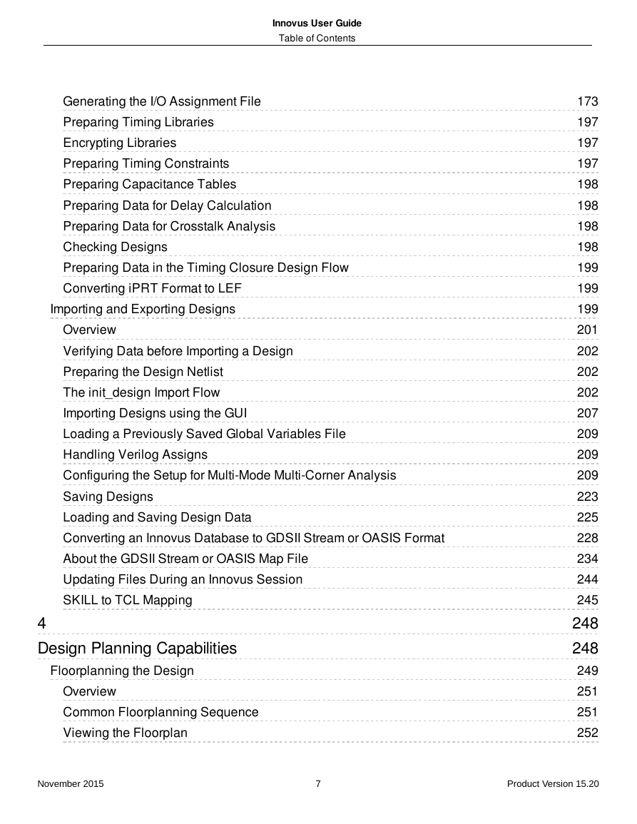
Generating the I/O Assignment File
Preparing Timing Libraries
Encrypting Libraries
Preparing Timing Constraints
Preparing Capacitance Tables
Preparing Data for Delay Calculation
Preparing Data for Crosstalk Analysis
Checking Designs
Preparing Data in the Timing Closure Design Flow
Converting iPRT Format to LEF
Importing and Exporting Designs
Overview
Verifying Data before Importing a Design
Preparing the Design Netlist
The init_design Import Flow
Importing Designs using the GUI
Loading a Previously Saved Global Variables File
Handling Verilog Assigns
Configuring the Setup for Multi-Mode Multi-Corner Analysis
Saving Designs
Loading and Saving Design Data
Converting an Innovus Database to GDSII Stream or OASIS Format
About the GDSII Stream or OASIS Map File
Updating Files During an Innovus Session
SKILL to TCL Mapping
4
Design Planning Capabilities
Floorplanning the Design
Overview
Common Floorplanning Sequence
Viewing the Floorplan
173
197
197
197
198
198
198
198
199
199
199
201
202
202
202
207
209
209
209
223
225
228
234
244
245
248
248
249
251
251
252
November 2015
7
Product Version 15.20
�
Innovus User Guide
Table of Contents
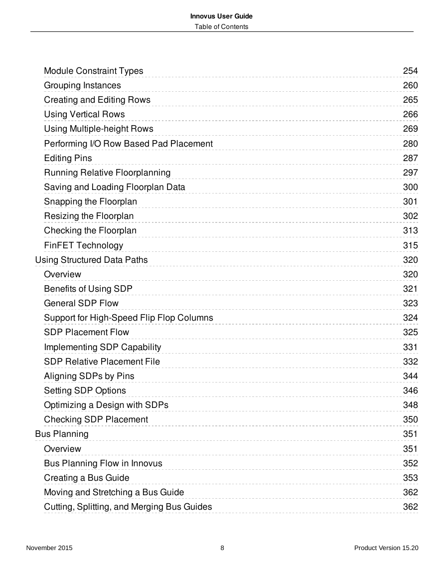
Module Constraint Types
Grouping Instances
Creating and Editing Rows
Using Vertical Rows
Using Multiple-height Rows
Performing I/O Row Based Pad Placement
Editing Pins
Running Relative Floorplanning
Saving and Loading Floorplan Data
Snapping the Floorplan
Resizing the Floorplan
Checking the Floorplan
FinFET Technology
Using Structured Data Paths
Overview
Benefits of Using SDP
General SDP Flow
Support for High-Speed Flip Flop Columns
SDP Placement Flow
Implementing SDP Capability
SDP Relative Placement File
Aligning SDPs by Pins
Setting SDP Options
Optimizing a Design with SDPs
Checking SDP Placement
Bus Planning
Overview
Bus Planning Flow in Innovus
Creating a Bus Guide
Moving and Stretching a Bus Guide
Cutting, Splitting, and Merging Bus Guides
254
260
265
266
269
280
287
297
300
301
302
313
315
320
320
321
323
324
325
331
332
344
346
348
350
351
351
352
353
362
362
November 2015
8
Product Version 15.20
�




 2023年江西萍乡中考道德与法治真题及答案.doc
 2012年重庆南川中考生物真题及答案.doc
 2013年江西师范大学地理学综合及文艺理论基础考研真题.doc
 2020年四川甘孜小升初语文真题及答案I卷.doc
 2020年注册岩土工程师专业基础考试真题及答案.doc
 2023-2024学年福建省厦门市九年级上学期数学月考试题及答案.doc
 2021-2022学年辽宁省沈阳市大东区九年级上学期语文期末试题及答案.doc
 2022-2023学年北京东城区初三第一学期物理期末试卷及答案.doc
 2018上半年江西教师资格初中地理学科知识与教学能力真题及答案.doc
 2012年河北国家公务员申论考试真题及答案-省级.doc
 2020-2021学年江苏省扬州市江都区邵樊片九年级上学期数学第一次质量检测试题及答案.doc
 2022下半年黑龙江教师资格证中学综合素质真题及答案.doc