【FPGA 设计实例】基于 FPGA 的数字示波器设计
Digital oscilloscope
A digital oscilloscope has many advantages over its analog counterpart, like the ability to
capture single events, and to display what happens before the trigger.
You can build a digital oscilloscope simply by hooking an ADC and an FPGA together.
This particular design uses an 100MHz flash ADC, so we are building an 100MSPS
(mega-samples-per-seconds) oscilloscope.
This oscilloscope design is interesting because it shows how powerful and useful modern
FPGAs can be. But if you are new to FPGA technology, keep that in mind this is not the easiest
design to understand on this site.
HDL design
Or how to create the oscilloscope logic inside the FPGA.
• HDL part 1 - FIFO-based design.
• HDL part 2 - RAM-based design.
• HDL part 3 - Trigger mechanism.
• HDL part 4 - More functionality.
Hardware
• This design was created using the Flashy boards.
• See also the "hands-on" page on how to build a simple oscilloscope.
Software
• History, features, screen shots.
• See also the interference patterns page.
Screenshot
Here's the view of a 27MHz signal, sampled at 100MHz and reconstructed using the "sample
equivalent time" technique.
�
Digital oscilloscope - part 1
Here's what is built here:
The FPGA receives 2 clocks:
• A slow "system" clock, fixed at 25MHz.
• An ADC sampling clock (something faster, let's say 100MHz), that is connected to
both the ADC and the FPGA.
Having these 2 clocks gives flexibility to the design. But that also means we need a way to
transfer information from one clock domain to the other. To validate that the hardware works,
�
let's go the easy route and use a FIFO. The acquired samples from the ADC are stored in the
FPGA FIFO at full ADC speed (100MHz).
Then, the FIFO content is read back, serialized and sent on a serial port at a much slower
speed (115200 baud). Finally we connect the serial output to a PC that receives each byte and
displays a signal trace.
For this first attempt, there is no trace triggering mechanism. The ADC storage starts at
random intervals so the trace will jump left and right, but that's fine for now.
Design considerations
At 100MHz, the FIFO fills up in about 10us. That's pretty fast. Once full, we have to stop
feeding it. What is stored needs to be completely sent to the PC before we can start feeding
the FIFO again.
The serial communication used here works at 115200 bauds, so roughly 10KBytes/s. 1024
samples take about 100ms to transmit. During that time, the oscilloscope is "blind", because
we discard the data coming from the ADC. So it is blind 99.99% of the time. That's typical of
this type of architecture.
That can be partially compensated when we add a trigger mechanism later, because while the
trigger is armed, it works at full ADC speed and can stay armed as long as it takes for the
trigger condition to happen. More on that later.
Register the inputs
The ADC output data bus is connected to the FPGA using 8 pins that we call "data_flash[7:0]".
These come at speed of up to 100MHz. Since this is fast, it is best to "register" them right
when they come in the FPGA.
reg [7:0] data_flash_reg;
always @(posedge clk_flash) data_flash_reg <= data_flash;
Now "data_flash_reg" is fully internal to the FPGA and can be fed to the FPGA FIFO.
The FIFO
The FIFO is 1024 words deep x 8 bits wide. Since we receive 8 bits per clock from the ADC,
we can store 1024 ADC samples. At 100MHz, it takes about 10us to fill up the FIFO.
�
The FIFO uses synchronous static RAM blocks available inside the FPGA. Each storage block
can store typically 512x8bits. So the FIFO uses 2 blocks.
The FIFO logic itself is created by using the FPGA vendor "function builder". Xilinx calls it
"coregen" while Altera "Megafunctions wizard". Here let's use Altera's Quartus to create this
file.
So now, using the FIFO is just a connectivity issue.
fifo
myfifo(.data(data_flash_reg), .wrreq(wrreq), .wrclk(clk_flash), .wrfull(wrfull), .wrempty(w
rempty), .q(q_fifo), .rdreq(rdreq), .rdclk(clk), .rdempty(rdempty));
Using a FIFO is nice because it takes care of the different clocks. We connected the write side
of the FIFO to the "clk_flash" (100MHz), and the read side of the FIFO to "clk" (25MHz).
The FIFO provides the full and empty signals for each clock domain. For example, "wrempty"
is an empty signal that can be used in the write clock domain ("clk_flash"), and "rdempty" can
be used in the read clock domain ("clk").
Using the FIFO is simple: Writing to it is just a matter of asserting the "wrreq" signal (and
providing the data to the ".data" port), while reading from it a matter of asserting "rdreq"
(and the data comes on the ".q" port).
Writing to the FIFO
To start writing to the FIFO, we wait until it is empty. Of course, at power-up (after the FPGA
is configured), that is true.
We stop only when it gets full. And then the process starts again... we wait until it is empty...
feed it until it is full... stop.
reg fillfifo;
always @(posedge clk_flash)
if(~fillfifo)
fillfifo <= wrempty; // start when empty
else
fillfifo <= ~wrfull; // stop when full
assign wrreq = fillfifo;
Reading to the FIFO
�
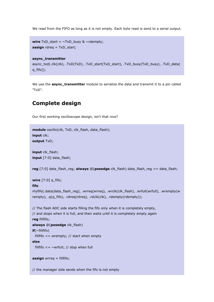
We read from the FIFO as long as it is not empty. Each byte read is send to a serial output.
wire TxD_start = ~TxD_busy & ~rdempty;
assign rdreq = TxD_start;
async_transmitter
async_txd(.clk(clk), .TxD(TxD), .TxD_start(TxD_start), .TxD_busy(TxD_busy), .TxD_data(
q_fifo));
We use the async_transmitter module to serialize the data and transmit it to a pin called
"TxD".
Complete design
Our first working oscilloscope design, isn't that nice?
module oscillo(clk, TxD, clk_flash, data_flash);
input clk;
output TxD;
input clk_flash;
input [7:0] data_flash;
reg [7:0] data_flash_reg; always @(posedge clk_flash) data_flash_reg <= data_flash;
wire [7:0] q_fifo;
fifo
myfifo(.data(data_flash_reg), .wrreq(wrreq), .wrclk(clk_flash), .wrfull(wrfull), .wrempty(w
rempty), .q(q_fifo), .rdreq(rdreq), .rdclk(clk), .rdempty(rdempty));
// The flash ADC side starts filling the fifo only when it is completely empty,
// and stops when it is full, and then waits until it is completely empty again
reg fillfifo;
always @(posedge clk_flash)
if(~fillfifo)
fillfifo <= wrempty; // start when empty
else
fillfifo <= ~wrfull; // stop when full
assign wrreq = fillfifo;
// the manager side sends when the fifo is not empty
�
wire TxD_busy;
wire TxD_start = ~TxD_busy & ~rdempty;
assign rdreq = TxD_start;
async_transmitter
async_txd(.clk(clk), .TxD(TxD), .TxD_start(TxD_start), .TxD_busy(TxD_busy), .TxD_data(
q_fifo));
endmodule
Digital oscilloscope - part 2
The FIFO allowed us to get a working design very quickly.
But for our simple oscilloscope, it is overkill.
We need a mechanism to store data from one clock domain (100MHz) and read it in another
(25MHz). A simple dual-port RAM does that.
The disadvantage of not using a FIFO is that all the synchonization between the 2 clock
domains (that the FIFO was doing for us) has to be done "manually" now.
Trigger
The "FIFO based" oscilloscope design didn't have an explicit trigger mechanism.
Let's change that. Now the oscilloscope will be triggered everytime it receives a character
from the serial port. Of course, that's still not a very useful design, but we'll improved on that
later.
We receive data from the serial port:
wire [7:0] RxD_data;
async_receiver
async_rxd(.clk(clk), .RxD(RxD), .RxD_data_ready(RxD_data_ready), .RxD_data(RxD_data
));
Everytime a new character is received, "RxD_data_ready" goes high for one clock. We use
that to trigger the oscilloscope.
Synchronization
�
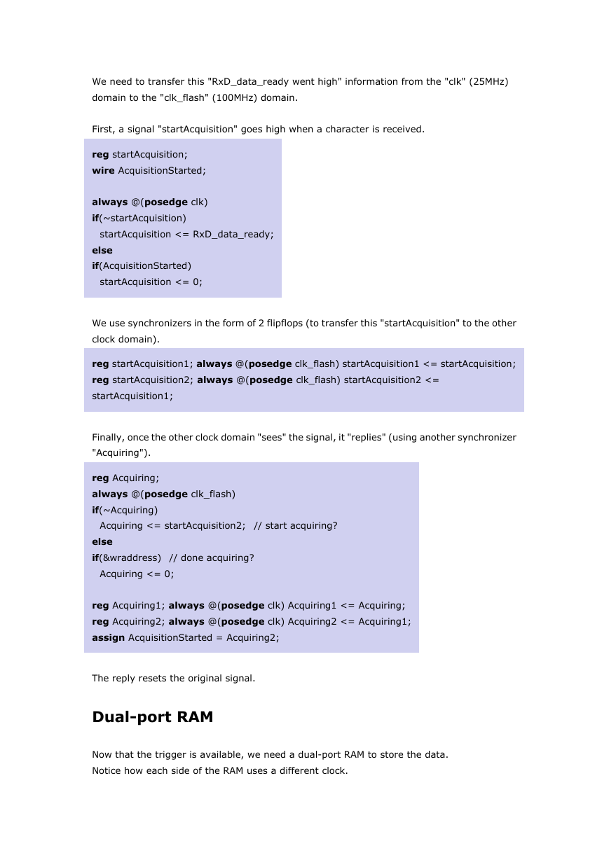
We need to transfer this "RxD_data_ready went high" information from the "clk" (25MHz)
domain to the "clk_flash" (100MHz) domain.
First, a signal "startAcquisition" goes high when a character is received.
reg startAcquisition;
wire AcquisitionStarted;
always @(posedge clk)
if(~startAcquisition)
startAcquisition <= RxD_data_ready;
else
if(AcquisitionStarted)
startAcquisition <= 0;
We use synchronizers in the form of 2 flipflops (to transfer this "startAcquisition" to the other
clock domain).
reg startAcquisition1; always @(posedge clk_flash) startAcquisition1 <= startAcquisition;
reg startAcquisition2; always @(posedge clk_flash) startAcquisition2 <=
startAcquisition1;
Finally, once the other clock domain "sees" the signal, it "replies" (using another synchronizer
"Acquiring").
reg Acquiring;
always @(posedge clk_flash)
if(~Acquiring)
Acquiring <= startAcquisition2; // start acquiring?
else
if(&wraddress) // done acquiring?
Acquiring <= 0;
reg Acquiring1; always @(posedge clk) Acquiring1 <= Acquiring;
reg Acquiring2; always @(posedge clk) Acquiring2 <= Acquiring1;
assign AcquisitionStarted = Acquiring2;
The reply resets the original signal.
Dual-port RAM
Now that the trigger is available, we need a dual-port RAM to store the data.
Notice how each side of the RAM uses a different clock.
�
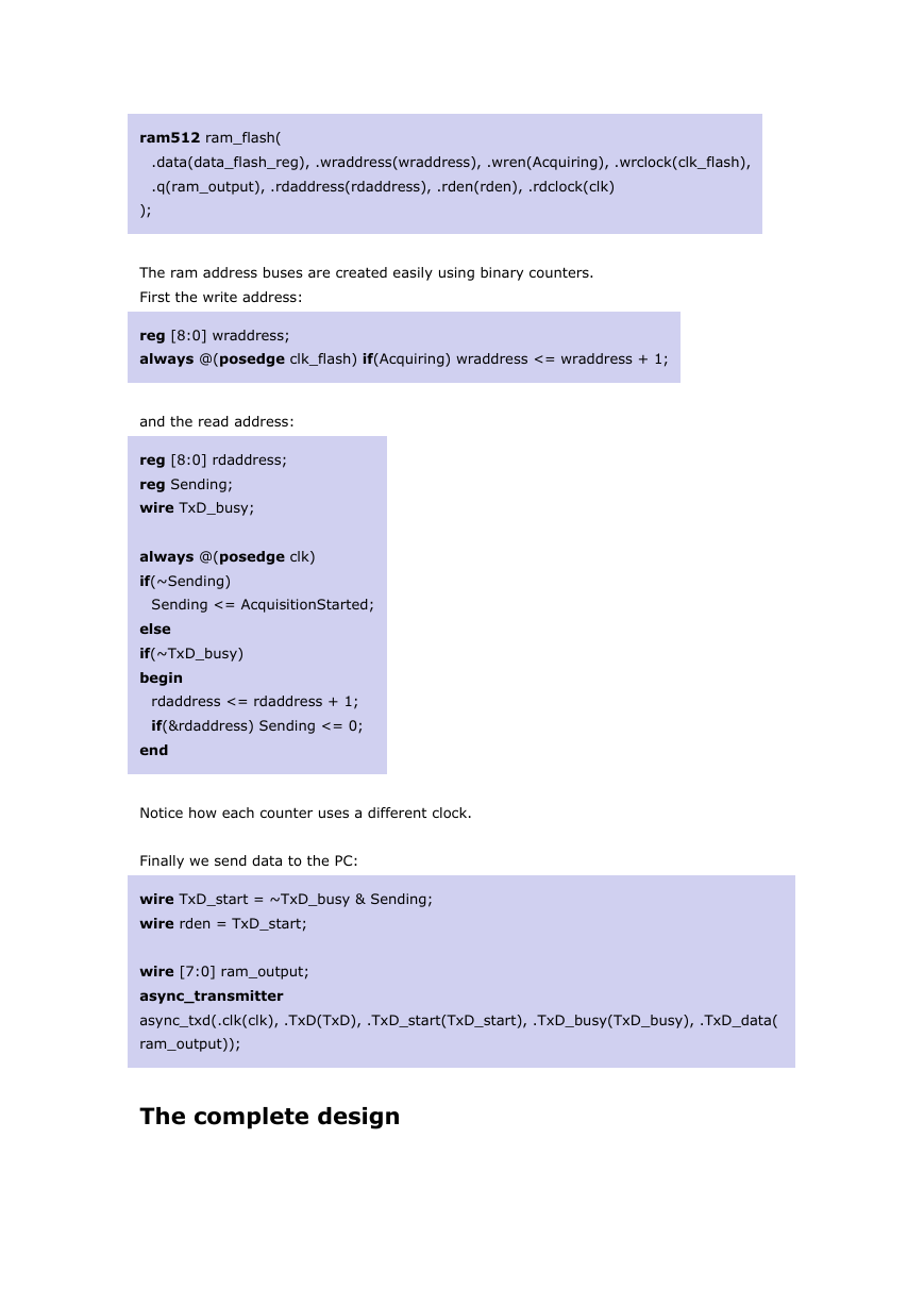
ram512 ram_flash(
.data(data_flash_reg), .wraddress(wraddress), .wren(Acquiring), .wrclock(clk_flash),
.q(ram_output), .rdaddress(rdaddress), .rden(rden), .rdclock(clk)
);
The ram address buses are created easily using binary counters.
First the write address:
reg [8:0] wraddress;
always @(posedge clk_flash) if(Acquiring) wraddress <= wraddress + 1;
and the read address:
reg [8:0] rdaddress;
reg Sending;
wire TxD_busy;
always @(posedge clk)
if(~Sending)
Sending <= AcquisitionStarted;
else
if(~TxD_busy)
begin
rdaddress <= rdaddress + 1;
if(&rdaddress) Sending <= 0;
end
Notice how each counter uses a different clock.
Finally we send data to the PC:
wire TxD_start = ~TxD_busy & Sending;
wire rden = TxD_start;
wire [7:0] ram_output;
async_transmitter
async_txd(.clk(clk), .TxD(TxD), .TxD_start(TxD_start), .TxD_busy(TxD_busy), .TxD_data(
ram_output));
The complete design
�



 2023年江西萍乡中考道德与法治真题及答案.doc
 2012年重庆南川中考生物真题及答案.doc
 2013年江西师范大学地理学综合及文艺理论基础考研真题.doc
 2020年四川甘孜小升初语文真题及答案I卷.doc
 2020年注册岩土工程师专业基础考试真题及答案.doc
 2023-2024学年福建省厦门市九年级上学期数学月考试题及答案.doc
 2021-2022学年辽宁省沈阳市大东区九年级上学期语文期末试题及答案.doc
 2022-2023学年北京东城区初三第一学期物理期末试卷及答案.doc
 2018上半年江西教师资格初中地理学科知识与教学能力真题及答案.doc
 2012年河北国家公务员申论考试真题及答案-省级.doc
 2020-2021学年江苏省扬州市江都区邵樊片九年级上学期数学第一次质量检测试题及答案.doc
 2022下半年黑龙江教师资格证中学综合素质真题及答案.doc