Description
FP6601Q
USB Dedicated Charging Port Controller for
Fast Charging Protocol and QC 2.0/3.0
®
is a
The FP6601Q
fast charging protocol
controller for HiSilicon Fast Charging Protocol
Quick ChargeTM 2.0/3.0
(FCP) and Qualcomm
(QC 2.0/3.0) USB
interface. The FP6601Q
monitors USB D+/D− data line and automatically
adjusts the output voltage depending on different
powered device (PD). The charging time of PD is
therefore optimized by the FP6601Q.
FP6601Q can support not only USB BC compliant
devices, but also Apple / Samsung / HUAWEI
devices and automatically detects whether a
connected powered device is QC 2.0/3.0 or FCP
capable
voltage
adjustment. If a PD is not compliant with QC
2.0/3.0 and FCP, the FP6601Q will disable the
adjustment of output voltage and keep the default
5V output voltage for safe operation.
enabling
before
output
The FP6601Q is available in a space-saving
SOT-23-6 package.
Features
● Supports HiSilicon Fast Charging Protocol (FCP)
● Supports Qualcomm
Quick ChargeTM 2.0/3.0
®
Class A : 3.6V up to 12V Output Voltage
● Automatically Selects FCP and QC2.0/3.0 Protocols
● Supports USB DCP Shorting D+ Line to D− Line per
USB Battery Charging Specification, Revision 1.2
● Complies with Chinese Telecommunication Industry
Standard YD/T 1591-2009
● Supports USB DCP Applying 2.7V on D+ Line
and 2.7V on D− Line
● SOT-23-6 Package
● UL Certification No. 4787452994-2
Applications
● Wall-Adapter, Smart Phones, Tablets, Notebooks
● Mobile / Tablet Power Bank
● Car Charger
● USB Power Output Ports
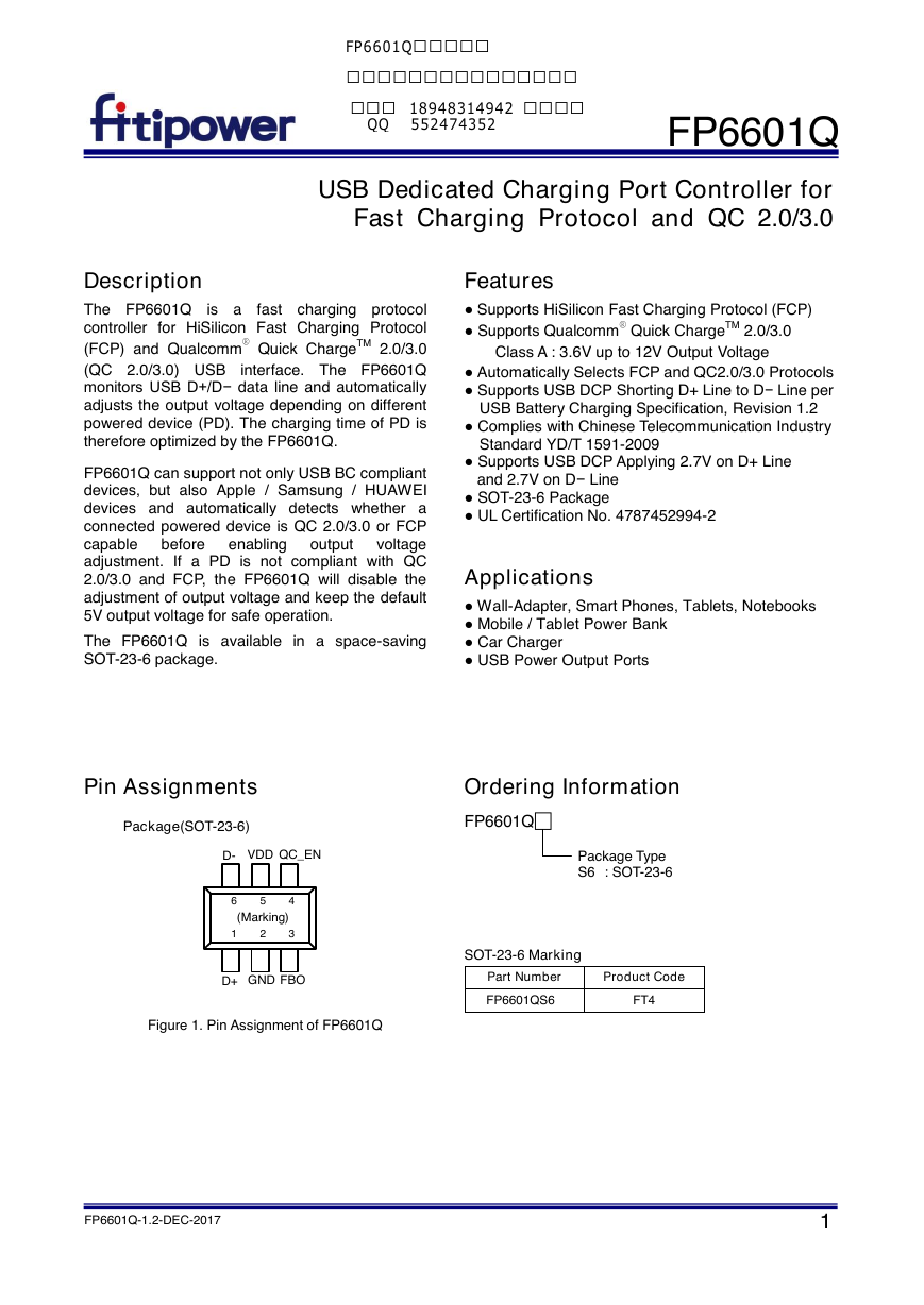
Pin Assignments
Ordering Information
Package(SOT-23-6)
D-
VDD
QC_EN
6
5
4
(Marking)
1
2
3
D+
GND FBO
Figure 1. Pin Assignment of FP6601Q
FP6601Q□
S
Package Type
S6 : SOT-23-6
SOT-23-6 Marking
Part Number
Product Code
FP6601QS6
FT4
FP6601Q-1.2-DEC-2017
1
�
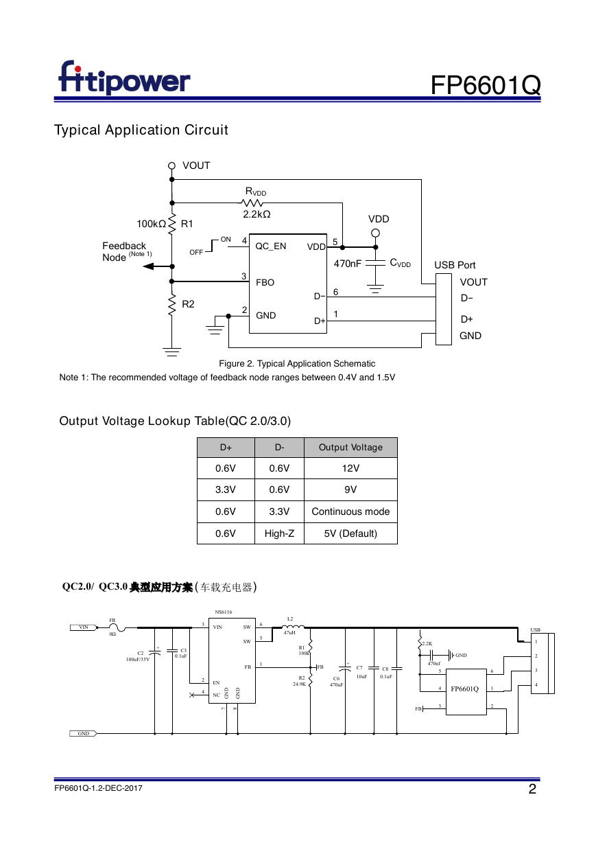
Typical Application Circuit
VOUT
FP6601Q
100k
Ω
R1
Feedback
Node (Note 1)
OFF
RVDD
2.2k
Ω
VDD
ON
4
QC_EN
5
VDD
470nF
CVDD
USB Port
R2
3
2
FBO
GND
6
1
D−
D+
Note 1: The recommended voltage of feedback node ranges between 0.4V and 1.5V
Figure 2. Typical Application Schematic
Output Voltage Lookup Table(QC 2.0/3.0)
VOUT
D−
D+
GND
D+
D-
Output Voltage
0.6V
0.6V
3.3V
0.6V
12V
9V
0.6V
3.3V
Continuous mode
0.6V
High-Z
5V (Default)
QC2.0/ QC3.0 典型应用方案
(
车载充电器
)
VIN
FR
0Ω
C2
100uF/35V
+
C3
0.1uF
6
5
1
SW
SW
FB
NS6116
3
VIN
2
4
EN
NC
D
N
G
D
N
G
7
8
L2
47uH
R1
100k
FB
+
R2
24.9K
C6
470uF
C7
10uF
C8
0.1uF
2.2K
470nf
5
4
3
FB
GND
FP6601Q
6
1
2
USB
1
2
3
4
GND
FP6601Q-1.2-DEC-2017
2
�
FP6601Q
Functional Pin Description
Pin Name
Pin No.
Pin Function
USB D+ data line. Recommended this pin connect without resistors(open) or with a resistor higher than
1MΩ connect to GND.
Ground pin.
Feedback output pin. Current Sink/Source FB Node.
QC_Enable: QC2.0/3.0 and FCP function are enabled by either logic high or high-Z. Contrarily,
QC2.0/3.0 and FCP function are disabled by logic low.
Power supply input pin.
USB D− data line.
D+
GND
FBO
QC_EN
VDD
D−
1
2
3
4
5
6
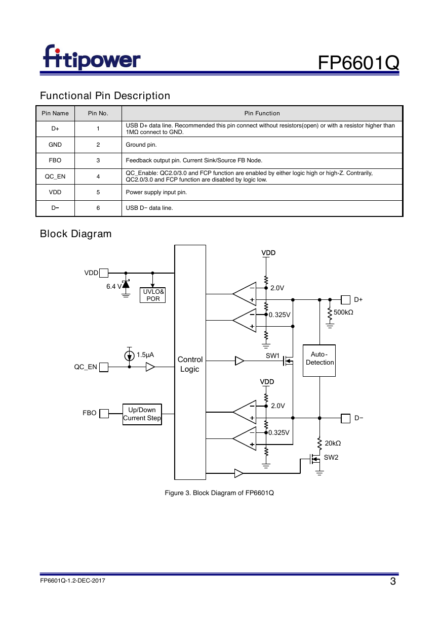
Block Diagram
VDD
6.4 V
UVLO &
POR
QC_EN
1.5μA
Control
Logic
FBO
Up/Down
Current Step
VDD
2.0V
0. 325V
SW1
VDD
2.0V
.0.325V
Figure 3. Block Diagram of FP6601Q
D+
500kΩ
Auto -
Detection
20kΩ
SW2
D−
FP6601Q-1.2-DEC-2017
3
�
FP6601Q
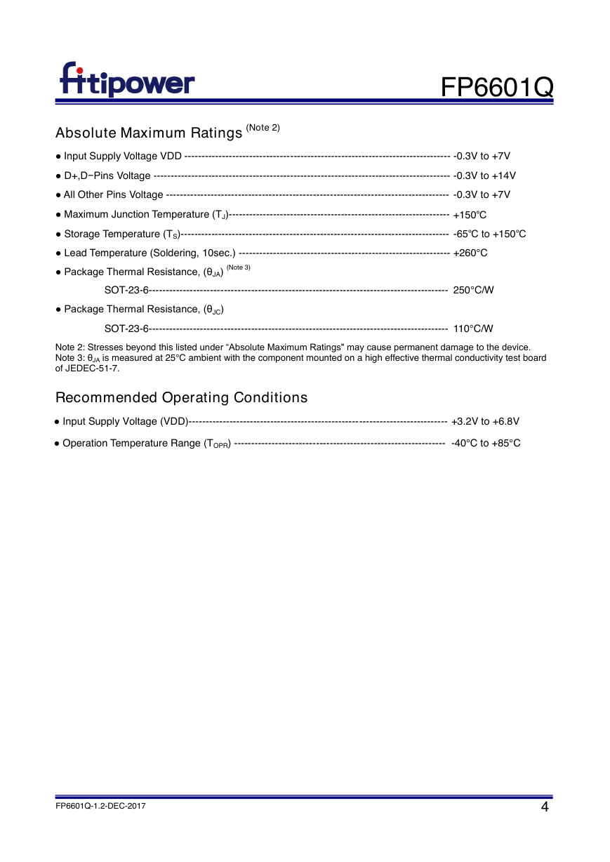
Absolute Maximum Ratings (Note 2)
● Input Supply Voltage VDD ------------------------------------------------------------------------------ -0.3V to +7V
● D+,D−Pins Voltage --------------------------------------------------------------------------------------- -0.3V to +14V
● All Other Pins Voltage ----------------------------------------------------------------------------------- -0.3V to +7V
● Maximum Junction Temperature (TJ)----------------------------------------------------------------- +150℃
● Storage Temperature (TS)------------------------------------------------------------------------------- -65℃ to +150℃
● Lead Temperature (Soldering, 10sec.) -------------------------------------------------------------- +260°C
● Package Thermal Resistance, (θJA) (Note 3)
SOT-23-6---------------------------------------------------------------------------------------- 250°C/W
● Package Thermal Resistance, (θJC)
SOT-23-6---------------------------------------------------------------------------------------- 110°C/W
Note 2: Stresses beyond this listed under “Absolute Maximum Ratings" may cause permanent damage to the device.
Note 3: θJA is measured at 25°C ambient with the component mounted on a high effective thermal conductivity test board
of JEDEC-51-7.
Recommended Operating Conditions
● Input Supply Voltage (VDD)---------------------------------------------------------------------------- +3.2V to +6.8V
● Operation Temperature Range (TOPR) -------------------------------------------------------------- -40°C to +85°C
FP6601Q-1.2-DEC-2017
4
�
FP6601Q
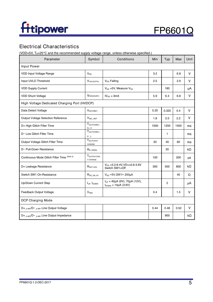
Electrical Characteristics
(VDD=5V, TA=25°C and the recommended supply voltage range, unless otherwise specified.)
Parameter
Symbol
Conditions
Min
Typ Max Unit
Input Power
VDD Input Voltage Range
VDD
Input UVLO Threshold
VUVLO(VTH)
VDD Falling
3.2
2.5
6.8
2.9
VDD Supply Current
VDD =5V, Measure VDD
180
VDD Shunt Voltage
VDD(SHUNT)
IVDD = 3mA
5.9
6.4
6.8
V
V
μA
V
V
V
0.25
0.325
0.4
1.8
2.0
2.2
1000
1250
1500 ms
20
1
40
20
ms
60
ms
kΩ
100
200
μs
High Voltage Dedicated Charging Port (HVDCP)
Data Detect Voltage
Output Voltage Selection Reference
D+ High Glitch Filter Time
D− Low Glitch Filter Time
Output Voltage Glitch Filter Time
D− Pull-Down Resistance
Continuous Mode Glitch Filter Time (Note 3)
D+ Leakage Resistance
VDAT(REF)
VSEL_REF
TGLITCH(BC)-
D+_H
TGLITCH(BC)-
D−_L
TGLITCH(V)
CHANGE
RD−(DWN)
TGLITCH-CON
T-CHANGE
RDAT-LKG
VDD =3.2-6.4V,VD+=0.6-3.6V
Switch SW1=Off
300
500
800
kΩ
Switch SW1 On-Resistance
RDS_ON_N1
VDD =5V,SW1= 200μA
Up/Down Current Step
IUP, IDOWN
IUP = 40μA (9V), 70μA (12V),
IDOWN = 14μA (3.6V)
Feedback Output Voltage
VFBO
DCP Charging Mode
D+_0.48V/D−_0.48V Line Output Voltage
D+_0.48V/D−_0.48V Line Output Impedance
0.4
2
40
Ω
μA
1.5
V
0.44
0.48
0.52
900
V
kΩ
FP6601Q-1.2-DEC-2017
5
�
FP6601Q
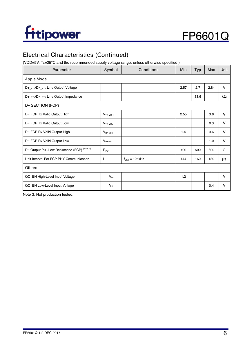
Electrical Characteristics (Continued)
(VDD=5V, TA=25°C and the recommended supply voltage range, unless otherwise specified.)
Parameter
Symbol
Conditions
Min
Typ Max Unit
Apple Mode
D+_2.7V/D−_2.7V Line Output Voltage
D+_2.7V/D−_2.7V Line Output Impedance
D− SECTION (FCP)
D− FCP Tx Valid Output High
D− FCP Tx Valid Output Low
D− FCP Rx Valid Output High
D− FCP Rx Valid Output Low
D− Output Pull-Low Resistance (FCP) (Note 4)
Unit Interval For FCP PHY Communication
Others
QC_EN High-Level Input Voltage
QC_EN Low-Level Input Voltage
Note 3: Not production tested.
VTX-VOH
VTX-VOL
VRX-VIH
VRX-VIL
RPD
UI
2.57
2.7
2.84
33.6
2.55
1.4
3.6
0.3
3.6
1.0
400
500
600
V
kΩ
V
V
V
V
Ω
fCLK = 125kHz
144
160
180
μs
VIH
VIL
1.2
0.4
V
V
FP6601Q-1.2-DEC-2017
6
�
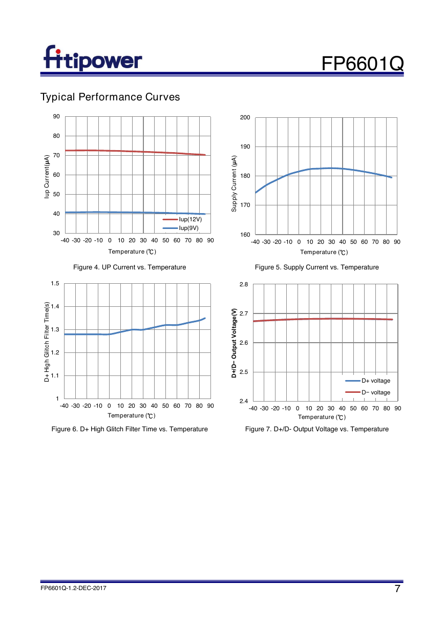
Typical Performance Curves
FP6601Q
)
A
μ
(
t
n
e
r
r
u
C
p
u
I
)
s
(
e
m
T
r
e
t
l
i
i
F
h
c
t
i
l
i
G
h
g
H
+
D
90
80
70
60
50
40
30
Iup(12V)
Iup(9V)
200
190
180
170
160
)
A
μ
(
t
n
e
r
r
u
C
y
p
p
u
S
l
-40 -30 -20 -10 0 10 20 30 40 50 60 70 80 90
-40 -30 -20 -10 0 10 20 30 40 50 60 70 80 90
Temperature (℃)
Figure 4. UP Current vs. Temperature
1.5
1.4
1.3
1.2
1.1
1
-40 -30 -20 -10 0 10 20 30 40 50 60 70 80 90
Temperature (℃)
Temperature (℃)
Figure 5. Supply Current vs. Temperature
D+ voltage
D− voltage
2.8
2.7
2.6
2.5
2.4
-40 -30 -20 -10 0 10 20 30 40 50 60 70 80 90
Temperature (℃)
)
V
(
e
g
a
t
l
o
V
t
u
p
t
u
O
−
D
+
D
/
Figure 6. D+ High Glitch Filter Time vs. Temperature
Figure 7. D+/D- Output Voltage vs. Temperature
FP6601Q-1.2-DEC-2017
7
�
FP6601Q
Application Information
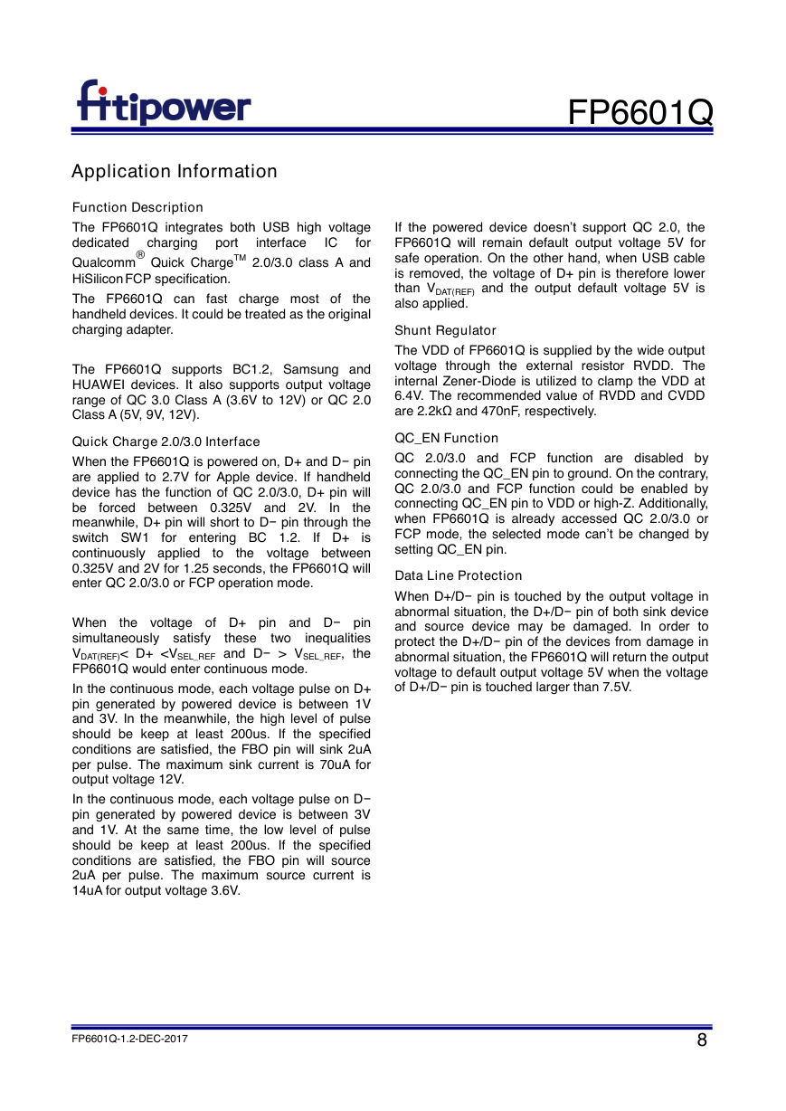
Function Description
The FP6601Q integrates both USB high voltage
charging port
dedicated
for
Quick ChargeTM 2.0/3.0 class A and
interface
IC
®
Qualcomm
HiSilicon FCP specification.
the
The FP6601Q can
handheld devices. It could be treated as the original
charging adapter.
fast charge most of
The FP6601Q supports BC1.2, Samsung and
HUAWEI devices. It also supports output voltage
range of QC 3.0 Class A (3.6V to 12V) or QC 2.0
Class A (5V, 9V, 12V).
If the powered device doesn’t support QC 2.0, the
FP6601Q will remain default output voltage 5V for
safe operation. On the other hand, when USB cable
is removed, the voltage of D+ pin is therefore lower
than VDAT(REF) and the output default voltage 5V is
also applied.
Shunt Regulator
The VDD of FP6601Q is supplied by the wide output
voltage through the external resistor RVDD. The
internal Zener-Diode is utilized to clamp the VDD at
6.4V. The recommended value of RVDD and CVDD
are 2.2kΩ and 470nF, respectively.
Quick Charge 2.0/3.0 Interface
QC_EN Function
QC 2.0/3.0 and FCP
function are disabled by
connecting the QC_EN pin to ground. On the contrary,
QC 2.0/3.0 and FCP function could be enabled by
connecting QC_EN pin to VDD or high-Z. Additionally,
when FP6601Q is already accessed QC 2.0/3.0 or
FCP mode, the selected mode can’t be changed by
setting QC_EN pin.
Data Line Protection
When D+/D− pin is touched by the output voltage in
abnormal situation, the D+/D− pin of both sink device
and source device may be damaged. In order to
protect the D+/D− pin of the devices from damage in
abnormal situation, the FP6601Q will return the output
voltage to default output voltage 5V when the voltage
of D+/D− pin is touched larger than 7.5V.
forced between 0.325V and 2V.
When the FP6601Q is powered on, D+ and D− pin
are applied to 2.7V for Apple device. If handheld
device has the function of QC 2.0/3.0, D+ pin will
be
the
meanwhile, D+ pin will short to D− pin through the
switch SW1
is
continuously applied
the voltage between
0.325V and 2V for 1.25 seconds, the FP6601Q will
enter QC 2.0/3.0 or FCP operation mode.
for entering BC 1.2.
If D+
to
In
When
the voltage of D+ pin and D− pin
simultaneously satisfy
inequalities
VDAT(REF)< D+ VSEL_REF, the
FP6601Q would enter continuous mode.
these
two
In the continuous mode, each voltage pulse on D+
pin generated by powered device is between 1V
and 3V. In the meanwhile, the high level of pulse
should be keep at least 200us. If the specified
conditions are satisfied, the FBO pin will sink 2uA
per pulse. The maximum sink current is 70uA for
output voltage 12V.
In the continuous mode, each voltage pulse on D−
pin generated by powered device is between 3V
and 1V. At the same time, the low level of pulse
should be keep at least 200us. If the specified
conditions are satisfied, the FBO pin will source
2uA per pulse. The maximum source current is
14uA for output voltage 3.6V.
FP6601Q-1.2-DEC-2017
8
�


 2023年江西萍乡中考道德与法治真题及答案.doc
 2012年重庆南川中考生物真题及答案.doc
 2013年江西师范大学地理学综合及文艺理论基础考研真题.doc
 2020年四川甘孜小升初语文真题及答案I卷.doc
 2020年注册岩土工程师专业基础考试真题及答案.doc
 2023-2024学年福建省厦门市九年级上学期数学月考试题及答案.doc
 2021-2022学年辽宁省沈阳市大东区九年级上学期语文期末试题及答案.doc
 2022-2023学年北京东城区初三第一学期物理期末试卷及答案.doc
 2018上半年江西教师资格初中地理学科知识与教学能力真题及答案.doc
 2012年河北国家公务员申论考试真题及答案-省级.doc
 2020-2021学年江苏省扬州市江都区邵樊片九年级上学期数学第一次质量检测试题及答案.doc
 2022下半年黑龙江教师资格证中学综合素质真题及答案.doc