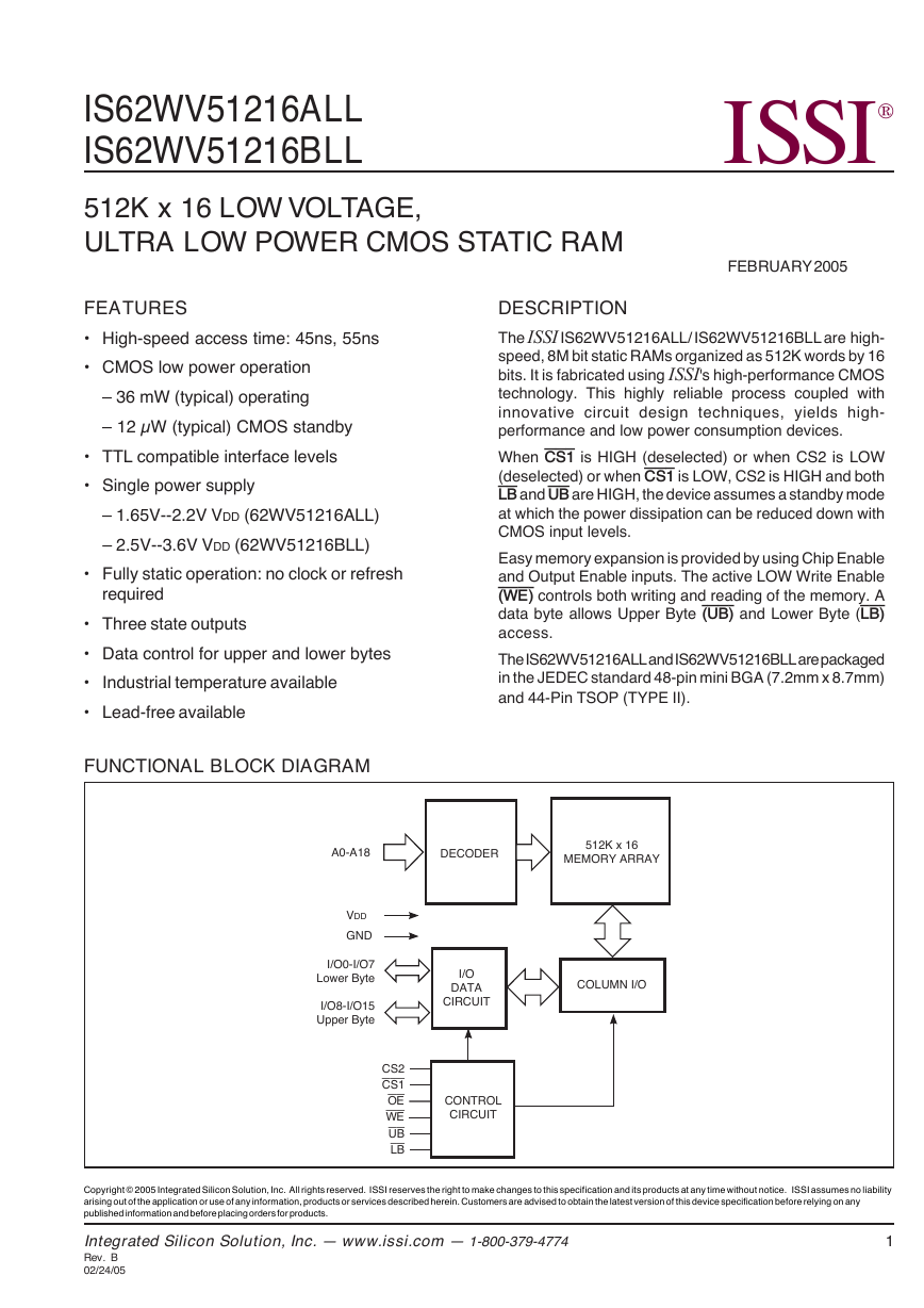
Integrated Silicon Solution, Inc. — www.issi.com — 1-800-379-47741Rev.B02/24/05IS62WV51216ALLIS62WV51216BLLISSI®Copyright © 2005 Integrated Silicon Solution, Inc. All rights reserved. ISSI reserves the right to make changes to this specification and its products at any time without notice. ISSI assumes no liabilityarising out of the application or use of any information, products or services described herein. Customers are advised to obtain the latest version of this device specification before relying on anypublished information and before placing orders for products.512K x 16 LOW VOLTAGE,ULTRA LOW POWER CMOS STATIC RAMFEATURES•High-speed access time: 45ns, 55nsCMOS low power operation– 36 mW (typical) operating– 12 µW (typical) CMOS standbyTTL compatible interface levelsSingle power supply– 1.65V--2.2V VDD (62WV51216ALL)– 2.5V--3.6V VDD (62WV51216BLL)Fully static operation: no clock or refreshrequiredThree state outputsData control for upper and lower bytesIndustrial temperature availableLead-free availableDESCRIPTIONThe ISSI IS62WV51216ALL/ IS62WV51216BLL are high-speed, 8M bit static RAMs organized as 512K words by 16bits. It is fabricated using ISSI's high-performance CMOStechnology. This highly reliable process coupled withinnovative circuit design techniques, yields high-performance and low power consumption devices.When CS1 is HIGH (deselected) or when CS2 is LOW(deselected) or when CS1 is LOW, CS2 is HIGH and bothLB and UB are HIGH, the device assumes a standby modeat which the power dissipation can be reduced down withCMOS input levels.Easy memory expansion is provided by using Chip Enableand Output Enable inputs. The active LOW Write Enable(WE) controls both writing and reading of the memory. Adata byte allows Upper Byte (UB) and Lower Byte (LB)access.The IS62WV51216ALL and IS62WV51216BLL are packagedin the JEDEC standard 48-pin mini BGA (7.2mm x 8.7mm)and 44-Pin TSOP (TYPE II).FUNCTIONAL BLOCK DIAGRAMFEBRUARY 2005A0-A18CS1OEWE512K x 16MEMORY ARRAYDECODERCOLUMN I/OCONTROLCIRCUITGNDVDDI/ODATACIRCUITI/O0-I/O7Lower ByteI/O8-I/O15Upper ByteUBLBCS2�
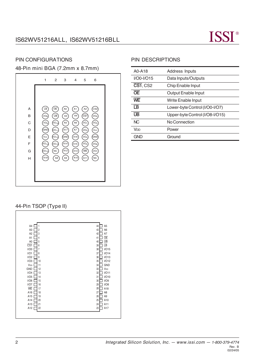
2Integrated Silicon Solution, Inc. — www.issi.com — 1-800-379-4774Rev.B02/24/05IS62WV51216ALL, IS62WV51216BLLISSI ®PIN CONFIGURATIONS48-Pin mini BGA (7.2mm x 8.7mm)PIN DESCRIPTIONSA0-A18Address InputsI/O0-I/O15Data Inputs/OutputsCS1, CS2Chip Enable InputOEOutput Enable InputWEWrite Enable InputLBLower-byte Control (I/O0-I/O7)UBUpper-byte Control (I/O8-I/O15)NCNo ConnectionVDDPowerGNDGround1 2 3 4 5 6ABCDEFGHLBOEA0A1A2CS2I/O8UBA3A4CS1I/O0I/O9I/O10A5A6I/O1I/O2GNDI/O11A17A7I/O3VDD`VDDI/O12GNDA16I/O4GNDI/O14I/O13A14A15I/O5I/O6I/O15NCA12A13WEI/O7A18A8A9A10A11NC1234567891011121314151617181920212244434241403938373635343332313029282726252423A4A3A2A1A0CS1I/O0I/O1I/O2I/O3VDDGNDI/O4I/O5I/O6I/O7WEA16A15A14A13A12A5A6A7OEUBLBI/O15I/O14I/O13I/O12GNDVDDI/O11I/O10I/O9I/O8A18A8A9A10A11A1744-Pin TSOP (Type II)�
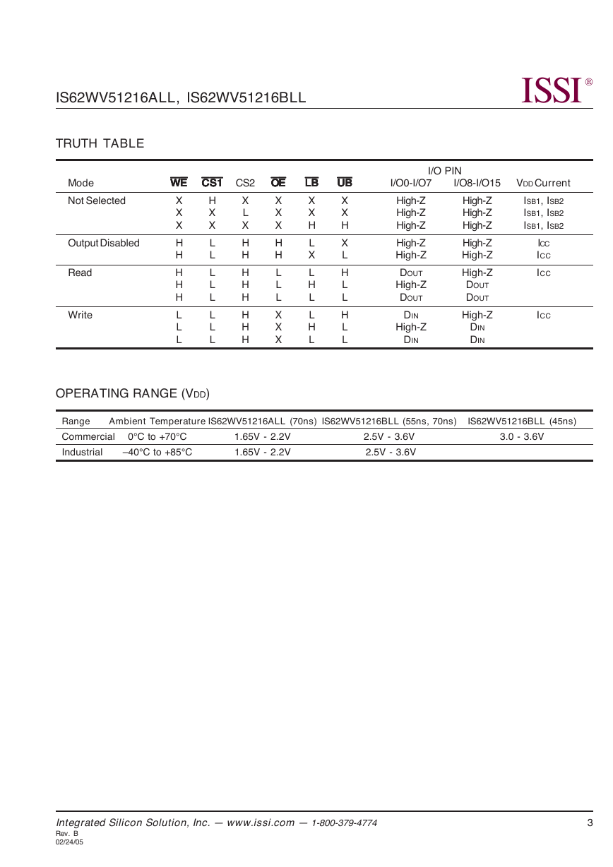
Integrated Silicon Solution, Inc. — www.issi.com — 1-800-379-47743Rev.B02/24/05IS62WV51216ALL, IS62WV51216BLLISSI ®TRUTH TABLEI/O PINModeWEWEWEWEWECS1CS1CS1CS1CS1CS2OEOEOEOEOELBLBLBLBLBUBUBUBUBUBI/O0-I/O7I/O8-I/O15VDD CurrentNot SelectedXHXXXXHigh-ZHigh-ZISB1, ISB2XXLXXXHigh-ZHigh-ZISB1, ISB2XXXXHHHigh-ZHigh-ZISB1, ISB2Output DisabledHLHHLXHigh-ZHigh-ZICCHLHHXLHigh-ZHigh-ZICCReadHLHLLHDOUTHigh-ZICCHLHLHLHigh-ZDOUTHLHLLLDOUTDOUTWriteLLHXLHDINHigh-ZICCLLHXHLHigh-ZDINLLHXLLDINDINOPERATING RANGE (VDD)RangeAmbient TemperatureIS62WV51216ALL (70ns)IS62WV51216BLL (55ns, 70ns)IS62WV51216BLL (45ns)Commercial0°C to +70°C1.65V - 2.2V2.5V - 3.6V3.0 - 3.6VIndustrial–40°C to +85°C1.65V - 2.2V 2.5V - 3.6V�
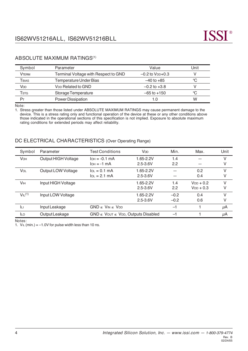
4Integrated Silicon Solution, Inc. — www.issi.com — 1-800-379-4774Rev.B02/24/05IS62WV51216ALL, IS62WV51216BLLISSI ®DC ELECTRICAL CHARACTERISTICS (Over Operating Range)SymbolParameterTest ConditionsVDDMin.Max.UnitVOHOutput HIGH VoltageIOH = -0.1 mA1.65-2.2V1.4—VIOH = -1 mA2.5-3.6V2.2—VVOLOutput LOW VoltageIOL = 0.1 mA1.65-2.2V—0.2VIOL = 2.1 mA2.5-3.6V—0.4VVIHInput HIGH Voltage1.65-2.2V1.4VDD + 0.2V2.5-3.6V2.2VDD + 0.3VVIL(1)Input LOW Voltage1.65-2.2V–0.20.4V2.5-3.6V–0.20.6VILIInput LeakageGND ≤ VIN ≤ VDD–11µAILOOutput LeakageGND ≤ VOUT ≤ VDD, Outputs Disabled–11µANotes:1.VIL (min.) = –1.0V for pulse width less than 10 ns.ABSOLUTE MAXIMUM RATINGS(1)SymbolParameterValueUnitVTERMTerminal Voltage with Respect to GND–0.2 to VDD+0.3VTBIASTemperature Under Bias–40 to +85°CVDDVDD Related to GND–0.2 to +3.8VTSTGStorage Temperature–65 to +150°CPTPower Dissipation1.0WNote:1.Stress greater than those listed under ABSOLUTE MAXIMUM RATINGS may cause permanent damage to thedevice. This is a stress rating only and functional operation of the device at these or any other conditions abovethose indicated in the operational sections of this specification is not implied. Exposure to absolute maximumrating conditions for extended periods may affect reliability.�
Integrated Silicon Solution, Inc. — www.issi.com — 1-800-379-47745Rev.B02/24/05IS62WV51216ALL, IS62WV51216BLLISSI ®AC TEST CONDITIONSParameter62WV51216ALL62WV51216BLL(Unit)(Unit)Input Pulse Level0.4V to VDD-0.20.4V to VDD-0.3VInput Rise and Fall Times5 ns5nsInput and Output TimingVREFVREFand Reference LevelOutput LoadSee Figures 1 and 2See Figures 1 and 2AC TEST LOADSFigure 1Figure 262WV51216ALL62WV51216BLL(1.65V - 2.2V)(2.5V - 3.6V)R1(Ω)30701029R2(Ω)31501728VREF0.9V1.5VVTM1.8V2.8VCAPACITANCE(1)SymbolParameterConditionsMax.UnitCINInput CapacitanceVIN = 0V8pFCOUTInput/Output CapacitanceVOUT = 0V10pFNote:1.Tested initially and after any design or process changes that may affect these parameters.R15 pFIncludingjig andscopeR2OUTPUTVTMR130 pFIncludingjig andscopeR2OUTPUTVTM�
6Integrated Silicon Solution, Inc. — www.issi.com — 1-800-379-4774Rev.B02/24/05IS62WV51216ALL, IS62WV51216BLLISSI ®IS62WV51216ALL, POWER SUPPLY CHARACTERISTICS(1) (Over Operating Range)SymbolParameterTest ConditionsMax.Unit70ICCVDD Dynamic OperatingVDD = Max.,Com.20mASupply CurrentIOUT = 0 mA, f = fMAXInd.25ICC1Operating SupplyVDD = Max., CS1 = 0.2VCom.4mACurrentWE = VDD – 0.2VInd.4CS2 = VDD – 0.2V, f = 1MHZISB1TTL Standby CurrentVDD = Max.,Com.0.3mA(TTL Inputs)VIN = VIH or VILInd.0.3CS1 = VIH , CS2 = VIL,f = 1 MHZORULB ControlVDD = Max., VIN = VIH or VILCS1 = VIL, f = 0, UB = VIH, LB = VIHISB2CMOS StandbyVDD = Max.,Com.15µACurrent (CMOS Inputs)CS1 ≥ VDD – 0.2V,Ind.21CS2 ≤ 0.2V,typ.(1)3VIN ≥ VDD – 0.2V, orVIN ≤ 0.2V, f = 0ORULB ControlVDD = Max., CS1 = VIL, CS2=VIHVIN ≥ VDD – 0.2V, or VIN ≤ 0.2V, f = 0;UB / LB = VDD – 0.2VNote:.1. Typical values are measured at VDD = 1.8V, TA = 25oC and not 100% tested.�
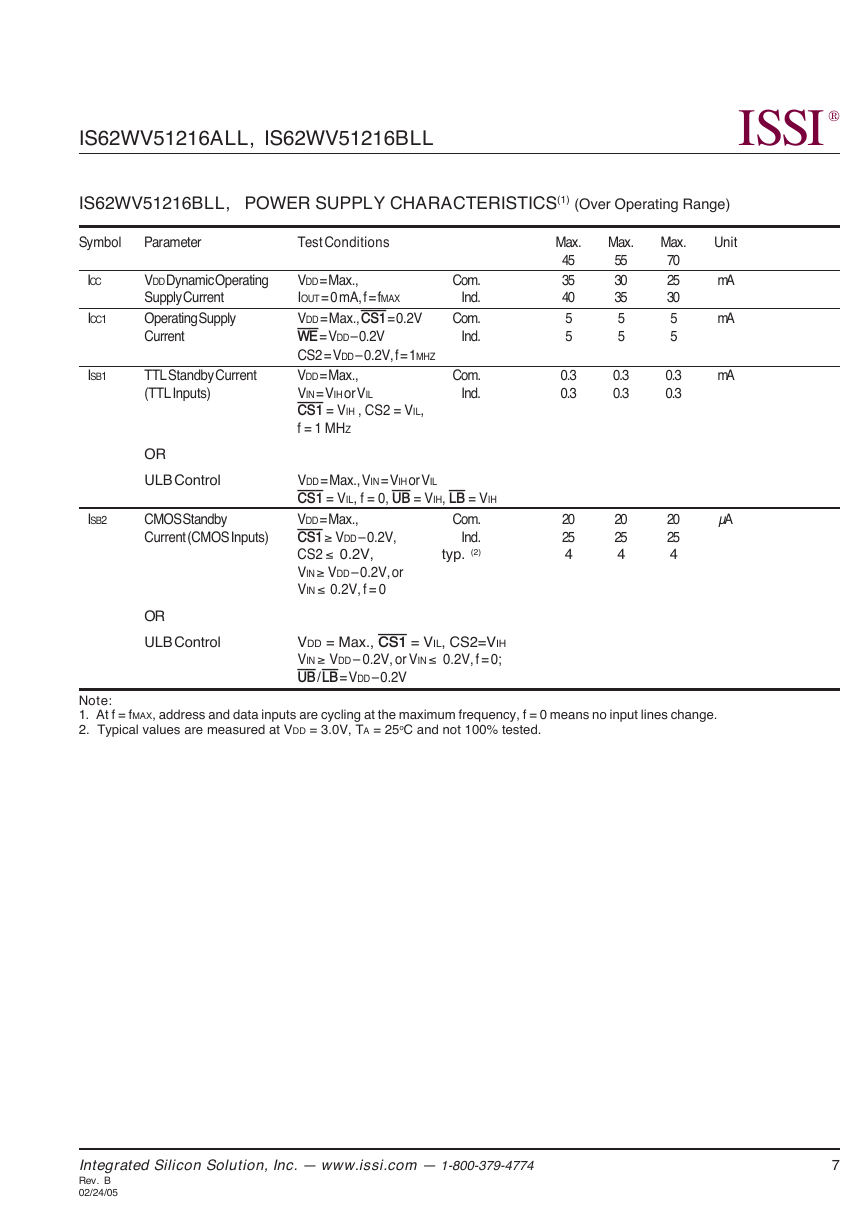
Integrated Silicon Solution, Inc. — www.issi.com — 1-800-379-47747Rev.B02/24/05IS62WV51216ALL, IS62WV51216BLLISSI ®IS62WV51216BLL, POWER SUPPLY CHARACTERISTICS(1) (Over Operating Range)SymbolParameterTest ConditionsMax.Max.Max.Unit455570ICCVDD Dynamic OperatingVDD = Max.,Com.353025mASupply CurrentIOUT = 0 mA, f = fMAXInd.403530ICC1Operating SupplyVDD = Max., CS1 = 0.2VCom.555mACurrentWE = VDD – 0.2VInd.555CS2 = VDD – 0.2V, f = 1MHZISB1TTL Standby CurrentVDD = Max.,Com.0.30.30.3mA(TTL Inputs)VIN = VIH or VILInd.0.30.30.3CS1 = VIH , CS2 = VIL,f = 1 MHZORULB ControlVDD = Max., VIN = VIH or VILCS1 = VIL, f = 0, UB = VIH, LB = VIHISB2CMOS StandbyVDD = Max.,Com.202020µACurrent (CMOS Inputs)CS1 ≥ VDD – 0.2V,Ind.252525CS2 ≤ 0.2V,typ. (2)444VIN ≥ VDD – 0.2V, orVIN ≤ 0.2V, f = 0ORULB ControlVDD = Max., CS1 = VIL, CS2=VIHVIN ≥ VDD – 0.2V, or VIN ≤ 0.2V, f = 0;UB / LB = VDD – 0.2VNote:1.At f = fMAX, address and data inputs are cycling at the maximum frequency, f = 0 means no input lines change.2. Typical values are measured at VDD = 3.0V, TA = 25oC and not 100% tested.�
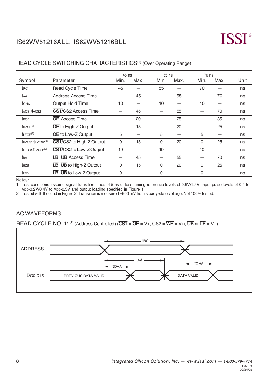
8Integrated Silicon Solution, Inc. — www.issi.com — 1-800-379-4774Rev.B02/24/05IS62WV51216ALL, IS62WV51216BLLISSI ®DATA VALIDPREVIOUS DATA VALIDtAAtOHAtOHAtRCDQ0-D15ADDRESSAC WAVEFORMSREAD CYCLE NO. 1(1,2) (Address Controlled) (CS1 = OE = VIL, CS2 = WE = VIH, UB or LB = VIL)READ CYCLE SWITCHING CHARACTERISTICS(1) (Over Operating Range)45 ns55 ns70 nsSymbolParameterMin.Max.Min.Max.Min.Max.UnittRCRead Cycle Time45—55—70—nstAAAddress Access Time—45—55—70nstOHAOutput Hold Time10—10—10—nstACS1/tACS2CS1/CS2 Access Time—45—55—70nstDOEOE Access Time—20—25—35nstHZOE(2)OE to High-Z Output—15—20—25nstLZOE(2)OE to Low-Z Output5—5—5—nstHZCS1/tHZCS2(2)CS1/CS2 to High-Z Output015020025nstLZCS1/tLZCS2(2)CS1/CS2 to Low-Z Output10—10—10—nstBALB, UB Access Time—45—55—70nstHZBLB, UB to High-Z Output015020025nstLZBLB, UB to Low-Z Output0—0—0—nsNotes:1.Test conditions assume signal transition times of 5 ns or less, timing reference levels of 0.9V/1.5V, input pulse levels of 0.4 toVDD-0.2V/0.4V to VDD-0.3V and output loading specified in Figure 1.2.Tested with the load in Figure 2. Transition is measured ±500 mV from steady-state voltage. Not 100% tested.�
