AVR100: Accessing the EEPROM
Features
• Random Read/Write
Sequential Read/Write
Runable Test/Example Program
Introduction
This application note contains routines for access of the EEPROM memory in the AVR
Microcontroller. Two types of Read/Write access has been implemented:
Random Read/Write: The user must set up both data and address before calling
the Read or Write routine.
Sequential Read/Write: The user needs only to set up the data to be
Read/Written. The current EEPROM address is automatically incremented prior to
access. The address has to be set prior to writing the first byte in a sequense.
The application note contains four routines which are described in detail in the follow-
ing sections. This application note contains routines for accessing the EEPROM in all
AVR devices.
Note: In the latest devices the EEWE bit in EECR is called EEPE, and the EEMWE is
called EEMPE. Also in the latest devices the EECR consist of two extra bits to set the
Programming Mode, EEPM0 and EEPM1. These two bits needs to be initialized
before EEPE is set.
EEdwr – Data to be written
EEawr – Address low byte to write
EEawrh – Address high byte to write
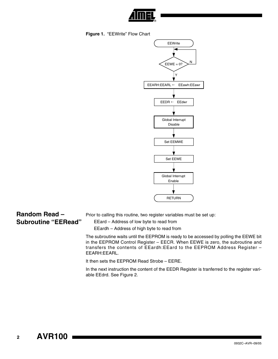
Random Write – Subroutine “EEWrite”
Three register variables must be set up prior to calling this routine:
The subroutine waits until the EEPROM is ready to be programmed by polling the
EEPROM Write Enable – EEWE bit in the EEPROM Control Register – EECR. When
EEWE is zero, the contents of EEdwr is transferred to the EEPROM Data Register –
EEDR, and the contents of EEawrh:EEawr is transferred to the EEPROM Address
Register – EEARH:EEARL. First the EEPROM Master Write Enable – EEMWE is set,
followed by the EEPROM write strobe EEWE in EECR. See Figure 1.
8-bit
Microcontroller
Application
Note
Rev. 0932C–AVR–09/05
1
�
Figure 1. “EEWrite” Flow Chart
EEWrite
EEWE = 0?
N
Y
EEARH:EEARL ! EEawh:EEawr
EEDR ! EEdwr
Global Interrupt
Disable
Set EEMWE
Set EEWE
Global Interrupt
Enable
RETURN
Random Read –
Subroutine “EERead”
Prior to calling this routine, two register variables must be set up:
EEard – Address of low byte to read from
EEardh – Address of high byte to read from
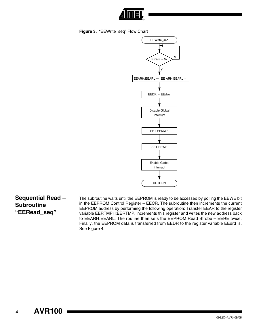
The subroutine waits until the EEPROM is ready to be accessed by polling the EEWE bit
in the EEPROM Control Register – EECR. When EEWE is zero, the subroutine and
transfers the contents of EEardh:EEard to the EEPROM Address Register –
EEARH:EEARL.
It then sets the EEPROM Read Strobe – EERE.
In the next instruction the content of the EEDR Register is tranferred to the register vari-
able EEdrd. See Figure 2.
2
AVR100
0932C–AVR–09/05
�
Figure 2. “EERead” Flow Chart
AVR100
EERead
EEWE = 0?
N
Y
EEARH:EEARL ! EEardh:EEard
SET EERE
EEdrd ! EEDR
RETURN
Sequential Write –
Subroutine
“EEWrite_seq”
Prior to calling this routine, one register variable must be set up:
EEdwr_s – Data to write
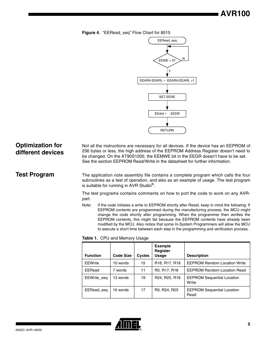
The subroutine waits until the EEPROM is ready to be programmed by polling the
EEWE bit in the EEPROM Control Register – EECR. When EEWE is zero and the con-
tents of the EEPROM Address Register – EEARH:EEARL are read into the register
variable EEWTMPH:EEWTMP. EEwtmp is incremented and written back to
EEARH:EEARL. This increments the current EEPROM address by one. The contents of
EEdwr is then transferred to the EEPROM Data Register – EEDR, before EEWE in
EECR is set, and then EEMWE is set. See Figure 3.
0932C–AVR–09/05
3
�
Figure 3. “EEWrite_seq” Flow Chart
EEWrite_seq
EEWE = 0?
N
Y
EEARH:EEARL ! EE ARH:EEARL +1
EEDR ! EEdwr
Disable Global
Interrupt
SET EEMWE
SET EEWE
Enable Global
Interrupt
RETURN
Sequential Read –
Subroutine
“EERead_seq”
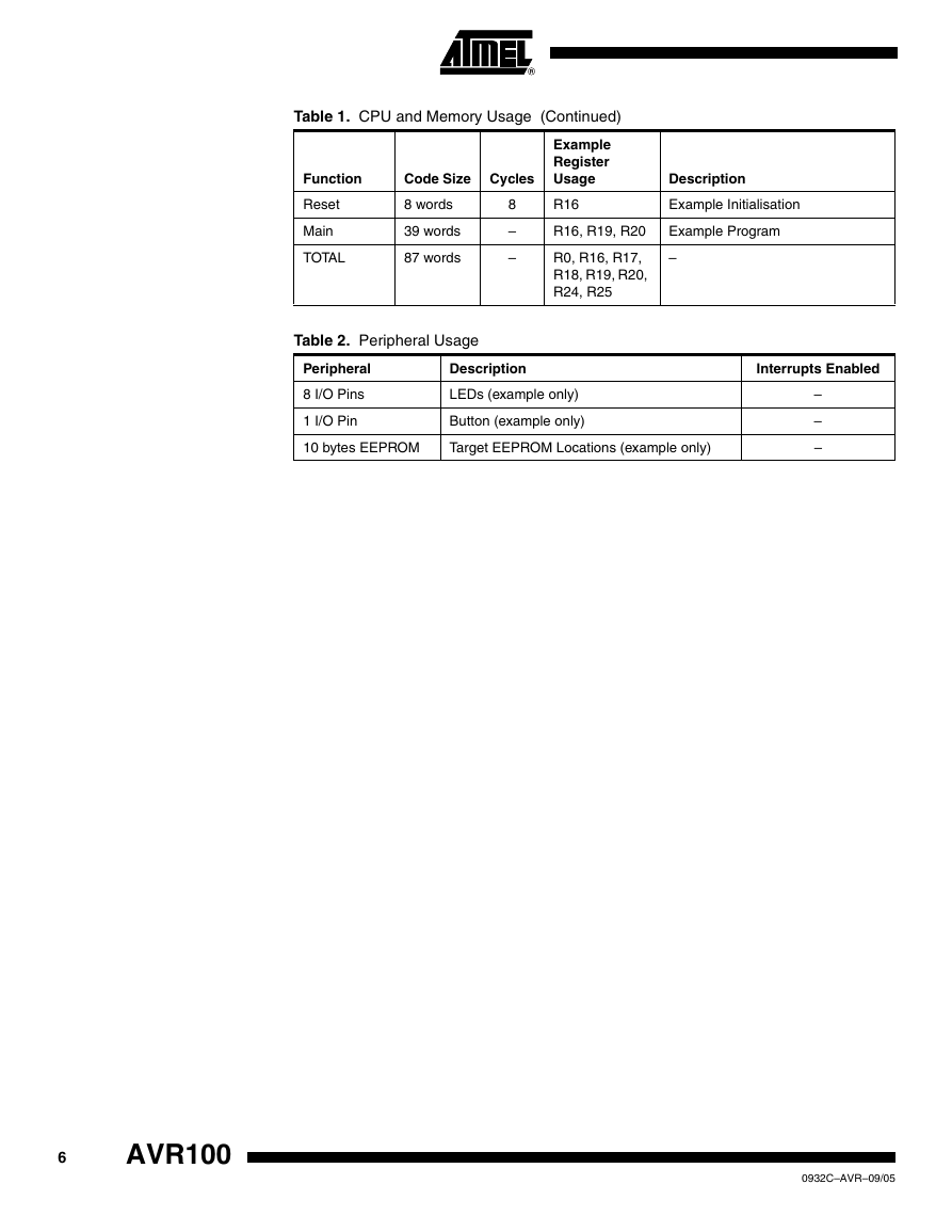
The subroutine waits until the EEPROM is ready to be accessed by polling the EEWE bit
in the EEPROM Control Register – EECR. The subroutine then increments the current
EEPROM address by performing the following operation: Transfer EEAR to the register
variable EERTMPH:EERTMP, increments this register and writes the new address back
to EEARH:EEARL. The routine then sets the EEPROM Read Strobe – EERE twice.
Finally, the EEPROM data is transferred from EEDR to the register variable EEdrd_s.
See Figure 4.
4
AVR100
0932C–AVR–09/05
�
Figure 4. “EERead_seq” Flow Chart for 8515
AVR100
EERead_seq
EEWE = 0?
N
Y
EEARH:EEARL ! EEARH:EEARL +1
SET EERE
EEdrd ! EEDR
RETURN
Optimization for
different devices
Test Program
Not all the instructions are necessary for all devices. If the device has an EEPROM of
256 bytes or less, the high address of the EEPROM Address Register doesn’t need to
be changed. On the AT90S1200, the EEMWE bit in the EEGR doesn’t have to be set.
See the section EEPROM Read/Write in the datasheet for further information.
The application note assembly file contains a complete program which calls the four
subroutines as a test of operation, and also as an example of usage. The test program
is suitable for running in AVR Studio®.
The test programs contains comments on how to port the code to work on any AVR-
part.
Note:
If the code initiates a write to EEPROM shortly after Reset, keep in mind the following: If
EEPROM contents are programmed during the manufacturing process, the MCU might
change the code shortly after programming. When the programmer then verifies the
EEPROM contents, this might fail because the EEPROM contents have already been
modified by the MCU. Also notice that some In-System Programmers will allow the MCU
to execute a short time between each step in the programming and verification process.
Table 1. CPU and Memory Usage
Function
Code Size Cycles
Example
Register
Usage
Description
EEWrite
EERead
10 words
7 words
EEWrite_seq
13 words
EERead_seq
10 words
15
11
19
17
R16, R17, R18
EEPROM Random Location Write
R0, R17, R18
EEPROM Random Location Read
R24, R25, R18
R0, R24, R25
EEPROM Sequential Location
Write
EEPROM Sequential Location
Read
0932C–AVR–09/05
5
�
Table 1. CPU and Memory Usage (Continued)
Function
Code Size Cycles
Reset
Main
TOTAL
8 words
39 words
87 words
8
–
–
Example
Register
Usage
R16
Description
Example Initialisation
R16, R19, R20
Example Program
R0, R16, R17,
R18, R19, R20,
R24, R25
–
Table 2. Peripheral Usage
Peripheral
8 I/O Pins
1 I/O Pin
Description
LEDs (example only)
Button (example only)
10 bytes EEPROM
Target EEPROM Locations (example only)
Interrupts Enabled
–
–
–
6
AVR100
0932C–AVR–09/05
�
RF/Automotive
Theresienstrasse 2
Postfach 3535
74025 Heilbronn, Germany
Tel: (49) 71-31-67-0
Fax: (49) 71-31-67-2340
1150 East Cheyenne Mtn. Blvd.
Colorado Springs, CO 80906, USA
Tel: 1(719) 576-3300
Fax: 1(719) 540-1759
Biometrics/Imaging/Hi-Rel MPU/
High Speed Converters/RF Datacom
Avenue de Rochepleine
BP 123
38521 Saint-Egreve Cedex, France
Tel: (33) 4-76-58-30-00
Fax: (33) 4-76-58-34-80
Atmel Corporation
Atmel Operations
2325 Orchard Parkway
San Jose, CA 95131, USA
Tel: 1(408) 441-0311
Fax: 1(408) 487-2600
Regional Headquarters
Europe
Atmel Sarl
Route des Arsenaux 41
Case Postale 80
CH-1705 Fribourg
Switzerland
Tel: (41) 26-426-5555
Fax: (41) 26-426-5500
Asia
Room 1219
Chinachem Golden Plaza
77 Mody Road Tsimshatsui
East Kowloon
Hong Kong
Tel: (852) 2721-9778
Fax: (852) 2722-1369
Japan
9F, Tonetsu Shinkawa Bldg.
1-24-8 Shinkawa
Chuo-ku, Tokyo 104-0033
Japan
Tel: (81) 3-3523-3551
Fax: (81) 3-3523-7581
Memory
2325 Orchard Parkway
San Jose, CA 95131, USA
Tel: 1(408) 441-0311
Fax: 1(408) 436-4314
Microcontrollers
2325 Orchard Parkway
San Jose, CA 95131, USA
Tel: 1(408) 441-0311
Fax: 1(408) 436-4314
La Chantrerie
BP 70602
44306 Nantes Cedex 3, France
Tel: (33) 2-40-18-18-18
Fax: (33) 2-40-18-19-60
ASIC/ASSP/Smart Cards
Zone Industrielle
13106 Rousset Cedex, France
Tel: (33) 4-42-53-60-00
Fax: (33) 4-42-53-60-01
1150 East Cheyenne Mtn. Blvd.
Colorado Springs, CO 80906, USA
Tel: 1(719) 576-3300
Fax: 1(719) 540-1759
Scottish Enterprise Technology Park
Maxwell Building
East Kilbride G75 0QR, Scotland
Tel: (44) 1355-803-000
Fax: (44) 1355-242-743
Literature Requests
www.atmel.com/literature
Disclaimer: The information in this document is provided in connection with Atmel products. No license, express or implied, by estoppel or otherwise, to any
intellectual property right is granted by this document or in connection with the sale of Atmel products. EXCEPT AS SET FORTH IN ATMEL’S TERMS AND CONDI-
TIONS OF SALE LOCATED ON ATMEL’S WEB SITE, ATMEL ASSUMES NO LIABILITY WHATSOEVER AND DISCLAIMS ANY EXPRESS, IMPLIED OR STATUTORY
WARRANTY RELATING TO ITS PRODUCTS INCLUDING, BUT NOT LIMITED TO, THE IMPLIED WARRANTY OF MERCHANTABILITY, FITNESS FOR A PARTICULAR
PURPOSE, OR NON-INFRINGEMENT. IN NO EVENT SHALL ATMEL BE LIABLE FOR ANY DIRECT, INDIRECT, CONSEQUENTIAL, PUNITIVE, SPECIAL OR INCIDEN-
TAL DAMAGES (INCLUDING, WITHOUT LIMITATION, DAMAGES FOR LOSS OF PROFITS, BUSINESS INTERRUPTION, OR LOSS OF INFORMATION) ARISING OUT
OF THE USE OR INABILITY TO USE THIS DOCUMENT, EVEN IF ATMEL HAS BEEN ADVISED OF THE POSSIBILITY OF SUCH DAMAGES. Atmel makes no
representations or warranties with respect to the accuracy or completeness of the contents of this document and reserves the right to make changes to specifications
and product descriptions at any time without notice. Atmel does not make any commitment to update the information contained herein. Unless specifically provided
otherwise, Atmel products are not suitable for, and shall not be used in, automotive applications. Atmel’s products are not intended, authorized, or warranted for use
as components in applications intended to support or sustain life.
© Atmel Corporation 2005. All rights reserved. Atmel®, logo and combinations thereof, Everywhere You Are®, AVR®, AVR Studio®, and others,
are registered trademarks or trademarks of Atmel Corporation or its subsidiaries. Other terms and product names may be trademarks of others.
Printed on recycled paper.
0932C–AVR–09/05
�




 2023年江西萍乡中考道德与法治真题及答案.doc
 2012年重庆南川中考生物真题及答案.doc
 2013年江西师范大学地理学综合及文艺理论基础考研真题.doc
 2020年四川甘孜小升初语文真题及答案I卷.doc
 2020年注册岩土工程师专业基础考试真题及答案.doc
 2023-2024学年福建省厦门市九年级上学期数学月考试题及答案.doc
 2021-2022学年辽宁省沈阳市大东区九年级上学期语文期末试题及答案.doc
 2022-2023学年北京东城区初三第一学期物理期末试卷及答案.doc
 2018上半年江西教师资格初中地理学科知识与教学能力真题及答案.doc
 2012年河北国家公务员申论考试真题及答案-省级.doc
 2020-2021学年江苏省扬州市江都区邵樊片九年级上学期数学第一次质量检测试题及答案.doc
 2022下半年黑龙江教师资格证中学综合素质真题及答案.doc