8
0
9
C
A
D
DAC908
DAC908
SBAS109B – JUNE 2003
8-Bit, 165MSPS
TM
DIGITAL-TO-ANALOG CONVERTER
FEATURES
G SINGLE +5V OR +3V OPERATION
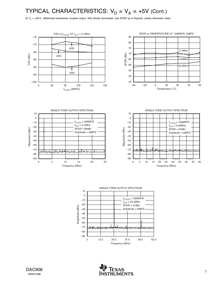
G HIGH SFDR: 5.04MHz Output at 100MSPS: 67dBc
G LOW GLITCH: 3pV-s
G LOW POWER: 170mW at +5V
G INTERNAL REFERENCE:
Optional Ext. Reference
Adjustable Full-Scale Range
Multiplying Option
DESCRIPTION
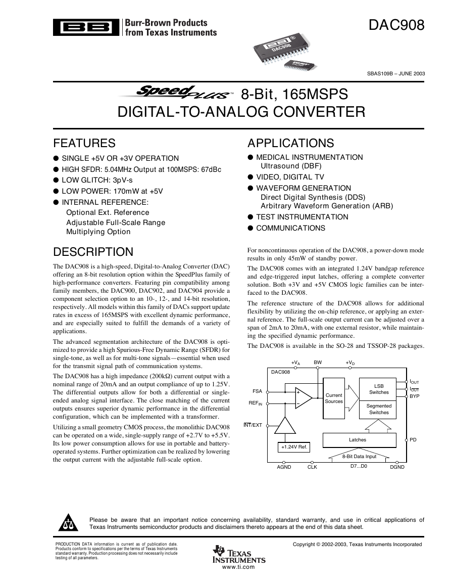
The DAC908 is a high-speed, Digital-to-Analog Converter (DAC)
offering an 8-bit resolution option within the SpeedPlus family of
high-performance converters. Featuring pin compatibility among
family members, the DAC900, DAC902, and DAC904 provide a
component selection option to an 10-, 12-, and 14-bit resolution,
respectively. All models within this family of DACs support update
rates in excess of 165MSPS with excellent dynamic performance,
and are especially suited to fulfill the demands of a variety of
applications.
The advanced segmentation architecture of the DAC908 is opti-
mized to provide a high Spurious-Free Dynamic Range (SFDR) for
single-tone, as well as for multi-tone signals—essential when used
for the transmit signal path of communication systems.
The DAC908 has a high impedance (200kΩ) current output with a
nominal range of 20mA and an output compliance of up to 1.25V.
The differential outputs allow for both a differential or single-
ended analog signal interface. The close matching of the current
outputs ensures superior dynamic performance in the differential
configuration, which can be implemented with a transformer.
Utilizing a small geometry CMOS process, the monolithic DAC908
can be operated on a wide, single-supply range of +2.7V to +5.5V.
Its low power consumption allows for use in portable and battery-
operated systems. Further optimization can be realized by lowering
the output current with the adjustable full-scale option.
APPLICATIONS
G MEDICAL INSTRUMENTATION
Ultrasound (DBF)
G VIDEO, DIGITAL TV
G WAVEFORM GENERATION
Direct Digital Synthesis (DDS)
Arbitrary Waveform Generation (ARB)
G TEST INSTRUMENTATION
G COMMUNICATIONS
For noncontinuous operation of the DAC908, a power-down mode
results in only 45mW of standby power.
The DAC908 comes with an integrated 1.24V bandgap reference
and edge-triggered input latches, offering a complete converter
solution. Both +3V and +5V CMOS logic families can be inter-
faced to the DAC908.
The reference structure of the DAC908 allows for additional
flexibility by utilizing the on-chip reference, or applying an exter-
nal reference. The full-scale output current can be adjusted over a
span of 2mA to 20mA, with one external resistor, while maintain-
ing the specified dynamic performance.
The DAC908 is available in the SO-28 and TSSOP-28 packages.
+VA
BW
+VD
DAC908
FSA
REFIN
INT/EXT
Current
Sources
IOUT
IOUT
BYP
LSB
Switches
Segmented
Switches
Latches
PD
+1.24V Ref.
AGND
CLK
D7...D0
DGND
8-Bit Data Input
Please be aware that an important notice concerning availability, standard warranty, and use in critical applications of
Texas Instruments semiconductor products and disclaimers thereto appears at the end of this data sheet.
PRODUCTION DATA information is current as of publication date.
Products conform to specifications per the terms of Texas Instruments
standard warranty. Production processing does not necessarily include
testing of all parameters.
www.ti.com
Copyright © 2002-2003, Texas Instruments Incorporated
�
ABSOLUTE MAXIMUM RATINGS
+VA to AGND ........................................................................ –0.3V to +6V
+VD to DGND ........................................................................ –0.3V to +6V
AGND to DGND ................................................................. –0.3V to +0.3V
+VA to +VD ............................................................................... –6V to +6V
CLK, PD to DGND ..................................................... –0.3V to VD + 0.3V
D0-D7 to DGND ......................................................... –0.3V to VD + 0.3V
IOUT, IOUT to AGND ........................................................ –1V to VA + 0.3V
BW, BYP to AGND ..................................................... –0.3V to VA + 0.3V
REFIN, FSA to AGND ................................................. –0.3V to VA + 0.3V
INT/EXT to AGND ...................................................... –0.3V to VA + 0.3V
Junction Temperature .................................................................... +150°C
Case Temperature ......................................................................... +100°C
Storage Temperature .................................................................... +125°C
PACKAGE/ORDERING INFORMATION
ELECTROSTATIC
DISCHARGE SENSITIVITY
This integrated circuit can be damaged by ESD. Texas Instru-
ments recommends that all integrated circuits be handled with
appropriate precautions. Failure to observe proper handling
and installation procedures can cause damage.
ESD damage can range from subtle performance degradation
to complete device failure. Precision integrated circuits may
be more susceptible to damage because very small parametric
changes could cause the device not to meet its published
specifications.
PRODUCT
DAC908U
"
DAC908E
"
PACKAGE
SO-28
"
TSSOP-28
"
PACKAGE
DRAWING
NUMBER
SPECIFIED
TEMPERATURE
RANGE
217
"
360
"
–40°C to +85°C
–40°C to +85°C
"
"
PACKAGE
MARKING
DAC908U
"
DAC908E
"
ORDERING
NUMBER(1)
DAC908U
DAC908U/1K
DAC908E
DAC908E/2K5
TRANSPORT
MEDIA
Rails
Tape and Reel
Rails
Tape and Reel
NOTE: (1) Models with a slash (/) are available only in Tape and Reel in the quantities indicated (e.g., /2K5 indicates 2500 devices per reel). Ordering 2500 pieces
of “DAC908E/2K5” will get a single 2500-piece Tape and Reel.
DEMO BOARD ORDERING INFORMATION
PRODUCT
DAC908U
DAC908E
DEMO BOARD
ORDERING NUMBER
COMMENT
DEM-DAC90xU
DEM-DAC908E
Populated evaluation board without DAC. Order sample of desired DAC90x model separately.
Populated evaluation board including the DAC908E.
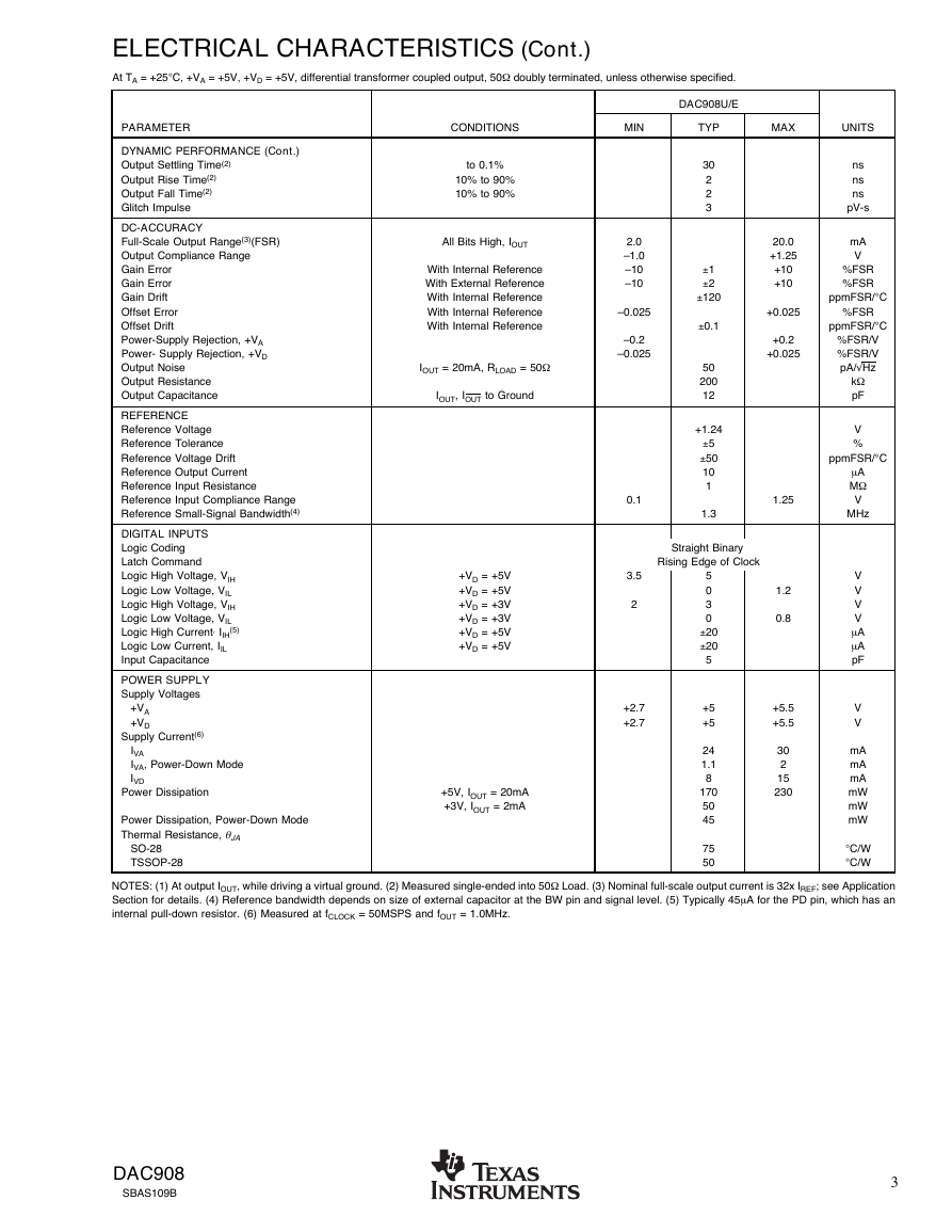
ELECTRICAL CHARACTERISTICS
At TA = full specified temperature range, +VA = +5V, +VD = +5V, differential transformer coupled output, 50Ω doubly terminated, unless otherwise specified.
PARAMETER
RESOLUTION
OUTPUT UPDATE RATE
Output Update Rate (fCLOCK)
Full Specified Temperature Range, Operating
STATIC ACCURACY(1)
Differential Nonlinearity (DNL)
Integral Nonlinearity (INL)
DYNAMIC PERFORMANCE
Spurious-Free Dynamic Range (SFDR)
fOUT = 1.0MHz, fCLOCK = 25MSPS
fOUT = 2.1MHz, fCLOCK = 50MSPS
fOUT = 5.04MHz, fCLOCK = 50MSPS
fOUT = 5.04MHz, fCLOCK = 100MSPS
fOUT = 20.2MHz, fCLOCK = 100MSPS
fOUT = 25.3MHz, fCLOCK = 125MSPS
fOUT = 41.5MHz, fCLOCK = 125MSPS
fOUT = 27.4MHz, fCLOCK = 165MSPS
fOUT = 54.8MHz, fCLOCK = 165MSPS
Spurious-Free Dynamic Range within a Window
fOUT = 2.1MHz, fCLOCK = 50MSPS
fOUT = 5.04MHz, fCLOCK = 100MSPS
Total Harmonic Distortion (THD)
fOUT = 2.1MHz, fCLOCK = 50MSPS
fOUT = 5.04MHz, fCLOCK = 100MSPS
fOUT = 20.2MHz, fCLOCK = 100MSPS
CONDITIONS
2.7V to 3.3V
4.5V to 5.5V
Ambient, TA
TA = +25°C
fCLOCK = 25MSPS, fOUT = 1.0MHz
TA = +25°C
To Nyquist
MIN
125
165
–40
–0.5
–0.5
64
2MHz Span
4MHz Span
MAX
+85
+0.5
+0.5
DAC908U/E
TYP
8
165
200
±0.25
±0.25
70
69
67
67
61
57
51
58
52
70
69
–72
–66
–60
UNITS
Bits
MSPS
MSPS
°C
LSB
LSB
dBc
dBc
dBc
dBc
dBc
dBc
dBc
dBc
dBc
dBc
dBc
dBc
dBc
dBc
2
DAC908
SBAS109B
�
ELECTRICAL CHARACTERISTICS (Cont.)
At TA = +25°C, +VA = +5V, +VD = +5V, differential transformer coupled output, 50Ω doubly terminated, unless otherwise specified.
DAC908U/E
PARAMETER
CONDITIONS
MIN
TYP
MAX
UNITS
DYNAMIC PERFORMANCE (Cont.)
Output Settling Time(2)
Output Rise Time(2)
Output Fall Time(2)
Glitch Impulse
DC-ACCURACY
Full-Scale Output Range(3)(FSR)
Output Compliance Range
Gain Error
Gain Error
Gain Drift
Offset Error
Offset Drift
Power-Supply Rejection, +VA
Power- Supply Rejection, +VD
Output Noise
Output Resistance
Output Capacitance
REFERENCE
Reference Voltage
Reference Tolerance
Reference Voltage Drift
Reference Output Current
Reference Input Resistance
Reference Input Compliance Range
Reference Small-Signal Bandwidth(4)
DIGITAL INPUTS
Logic Coding
Latch Command
Logic High Voltage, VIH
Logic Low Voltage, VIL
Logic High Voltage, VIH
Logic Low Voltage, VIL
Logic High Current, IIH
Logic Low Current, IIL
Input Capacitance
(5)
POWER SUPPLY
Supply Voltages
+VA
+VD
Supply Current(6)
IVA
IVA, Power-Down Mode
IVD
Power Dissipation
Power Dissipation, Power-Down Mode
Thermal Resistance, θJA
SO-28
TSSOP-28
to 0.1%
10% to 90%
10% to 90%
All Bits High, IOUT
With Internal Reference
With External Reference
With Internal Reference
With Internal Reference
With Internal Reference
IOUT = 20mA, RLOAD = 50Ω
IOUT, IOUT to Ground
+VD = +5V
+VD = +5V
+VD = +3V
+VD = +3V
+VD = +5V
+VD = +5V
+5V, IOUT = 20mA
+3V, IOUT = 2mA
2.0
–1.0
–10
–10
–0.025
–0.2
–0.025
0.1
3.5
2
+2.7
+2.7
30
2
2
3
±1
±2
±120
±0.1
50
200
12
+1.24
±5
±50
10
1
1.3
Straight Binary
Rising Edge of Clock
5
0
3
0
±20
±20
5
+5
+5
24
1.1
8
170
50
45
75
50
20.0
+1.25
+10
+10
+0.025
+0.2
+0.025
1.25
1.2
0.8
+5.5
+5.5
30
2
15
230
ns
ns
ns
pV-s
mA
V
%FSR
%FSR
ppmFSR/°C
%FSR
ppmFSR/°C
%FSR/V
%FSR/V
pA/√Hz
kΩ
pF
V
%
ppmFSR/°C
µA
MΩ
V
MHz
V
V
V
V
µA
µA
pF
V
V
mA
mA
mA
mW
mW
mW
°C/W
°C/W
NOTES: (1) At output IOUT, while driving a virtual ground. (2) Measured single-ended into 50Ω Load. (3) Nominal full-scale output current is 32x IREF; see Application
Section for details. (4) Reference bandwidth depends on size of external capacitor at the BW pin and signal level. (5) Typically 45µA for the PD pin, which has an
internal pull-down resistor. (6) Measured at fCLOCK = 50MSPS and fOUT = 1.0MHz.
DAC908
SBAS109B
3
�
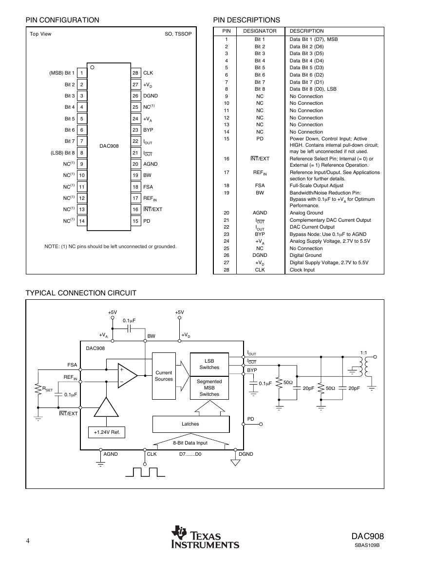
PIN CONFIGURATION
Top View
SO, TSSOP
(MSB) Bit 1
Bit 2
Bit 3
Bit 4
Bit 5
Bit 6
Bit 7
(LSB) Bit 8
NC(1)
NC(1)
NC(1)
NC(1)
NC(1)
NC(1)
1
2
3
4
5
6
7
8
9
10
11
12
13
14
DAC908
28
27
26
25
24
23
22
21
20
19
18
17
16
CLK
+VD
DGND
NC(1)
+VA
BYP
IOUT
IOUT
AGND
BW
FSA
REFIN
INT/EXT
15
PD
NOTE: (1) NC pins should be left unconnected or grounded.
PIN
1
2
3
4
5
6
7
8
9
10
11
12
13
14
15
16
17
18
19
20
21
22
23
24
25
26
27
28
PIN DESCRIPTIONS
DESIGNATOR
Bit 1
Bit 2
Bit 3
Bit 4
Bit 5
Bit 6
Bit 7
Bit 8
NC
NC
NC
NC
NC
NC
PD
INT/EXT
REFIN
FSA
BW
AGND
IOUT
IOUT
BYP
+VA
NC
DGND
+VD
CLK
DESCRIPTION
Data Bit 1 (D7), MSB
Data Bit 2 (D6)
Data Bit 3 (D5)
Data Bit 4 (D4)
Data Bit 5 (D3)
Data Bit 6 (D2)
Data Bit 7 (D1)
Data Bit 8 (D0), LSB
No Connection
No Connection
No Connection
No Connection
No Connection
No Connection
Power Down, Control Input; Active
HIGH. Contains internal pull-down circuit;
may be left unconnected if not used.
Reference Select Pin; Internal (= 0) or
External (= 1) Reference Operation.
Reference Input/Ouput. See Applications
section for further details.
Full-Scale Output Adjust
Bandwidth/Noise Reduction Pin:
Bypass with 0.1µF to +VA for Optimum
Performance.
Analog Ground
Complementary DAC Current Output
DAC Current Output
Bypass Node: Use 0.1µF to AGND
Analog Supply Voltage, 2.7V to 5.5V
No Connection
Digital Ground
Digital Supply Voltage, 2.7V to 5.5V
Clock Input
TYPICAL CONNECTION CIRCUIT
+5V
0.1µF
+5V
BW
+VD
+VA
DAC908
Current
Sources
LSB
Switches
Segmented
MSB
Switches
+1.24V Ref.
Latches
8-Bit Data Input
RSET
FSA
REFIN
0.1µF
INT/EXT
1:1
0.1µF
50Ω
20pF
50Ω
20pF
IOUT
IOUT
BYP
PD
AGND
CLK
D7.......D0
DGND
4
DAC908
SBAS109B
�
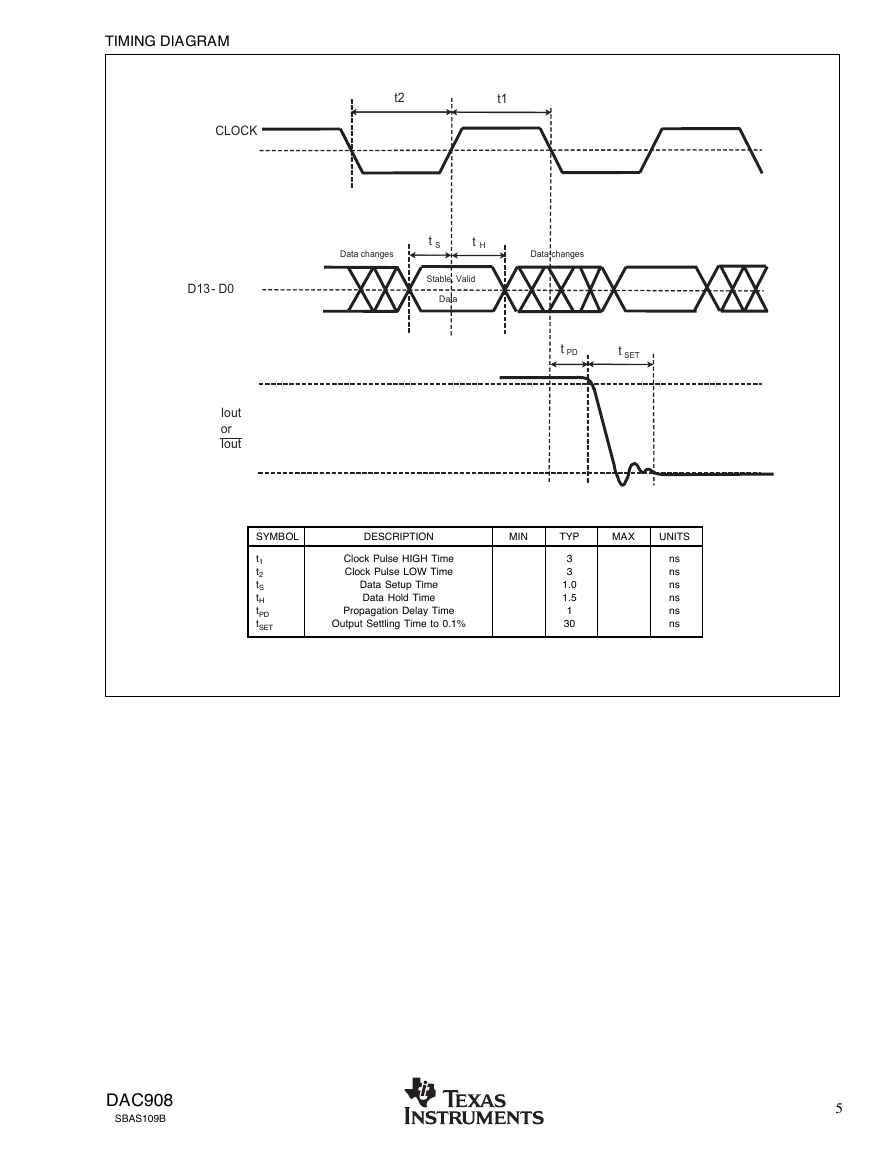
TIMING DIAGRAM
t2
t1
CLOCK
Data changes
t S
t H
Stable, Valid
Data
Data changes
t PD
t SET
D13 - D0
Iout
or
Iout
SYMBOL
DESCRIPTION
MIN
TYP
MAX
UNITS
t1
t2
tS
tH
tPD
tSET
Clock Pulse HIGH Time
Clock Pulse LOW Time
Data Setup Time
Data Hold Time
Propagation Delay Time
Output Settling Time to 0.1%
3
3
1.0
1.5
1
30
ns
ns
ns
ns
ns
ns
DAC908
SBAS109B
5
�
TYPICAL CHARACTERISTICS: VD = VA = +5V
At TA = +25°C, differential transformer coupled output, 50Ω doubly terminated, and SFDR up to Nyquist, unless otherwise noted.
)
c
B
d
(
R
D
F
S
)
c
B
d
(
R
D
F
S
)
c
B
d
(
R
D
F
S
85
80
75
70
65
60
55
85
80
75
70
65
60
55
50
45
80
75
70
65
60
55
50
45
40
6
SFDR vs fOUT AT 25MSPS
–6dBFS
0dBFS
)
c
B
d
(
R
D
F
S
85
80
75
70
65
60
55
SFDR vs fOUT AT 50MSPS
–6dBFS
0dBFS
0
2.0
4.0
6.0
8.0
10.0
12.0
0
5.0
Frequency (MHz)
10.0
15.0
Frequency (MHz)
20.0
25.0
SFDR vs fOUT AT 100MSPS
–6dBFS
0dBFS
SFDR vs fOUT AT 125MSPS
–6dBFS
0dBFS
)
c
B
d
(
R
D
F
S
85
80
75
70
65
60
55
50
45
0
10.0
20.0
30.0
Frequency (MHz)
40.0
50.0
0
10.0
20.0
30.0
40.0
50.0
60.0
Frequency (MHz)
SFDR vs fOUT AT 165MSPS
–6dBFS
0dBFS
0
10.0
20.0
40.0
30.0
50.0
Frequency (MHz)
60.0
70.0
80.0
)
c
B
d
(
R
D
F
S
80
75
70
65
60
55
50
45
40
X
2
SFDR vs IOUTFS and fOUT AT 100MSPS
2.1MHz
5.04MHz
20.2MHz
10.1MHz
X
40.4MHz
X
5
10
IOUTFS (mA)
X
20
DAC908
SBAS109B
�
TYPICAL CHARACTERISTICS: VD = VA = +5V (Cont.)
At TA = +25°C, differential transformer coupled output, 50Ω doubly terminated, and SFDR up to Nyquist, unless otherwise noted.
–70
–75
–80
–85
–90
–95
)
c
B
d
(
D
H
T
–100
0
)
m
B
d
(
e
d
u
t
i
n
g
a
M
10
0
–10
–20
–30
–40
–50
–60
–70
–80
–90
THD vs fCLOCK AT fOUT = 2.1MHz
2HD
3HD
X
25
X
X
4HD
50
100
fCLOCK (MSPS)
X
SFDR vs TEMPERATURE AT 100MSPS, 0dBFS
X
X
X
X
2.1MHz
5.04MHz
X
X
20.2MHz
X
)
c
B
d
(
R
D
F
S
85
80
75
70
65
60
55
50
45
125
150
–40
–20
0
25
50
Temperature (°C)
70
85
SINGLE-TONE OUTPUT SPECTRUM
SINGLE-TONE OUTPUT SPECTRUM
fCLOCK = 50MSPS
fOUT = 2.1MHz
SFDR = 69dBc
Amplitude = 0dBFS
)
m
B
d
(
e
d
u
t
i
n
g
a
M
10
0
–10
–20
–30
–40
–50
–60
–70
–80
–90
fCLOCK = 100MSPS
fOUT = 5.04MHz
SFDR = 67dBc
Amplitude = 0dBFS
0
5
10
15
20
25
0
5
10
15
20
25
30
35
40
45
50
Frequency (MHz)
Frequency (MHz)
SINGLE-TONE OUTPUT SPECTRUM
fCLOCK = 125MSPS
fOUT = 25.3MHz
SFDR = 57dBc
Amplitude = 0dBFS
)
m
B
d
(
e
d
u
t
i
n
g
a
M
10
0
–10
–20
–30
–40
–50
–60
–70
–80
–90
0
12.5
25.0
37.5
Frequency (MHz)
50.0
62.5
DAC908
SBAS109B
7
�
TYPICAL CHARACTERISTICS: VD = VA = +3V
At TA = +25°C, differential transformer coupled output, 50Ω doubly terminated, and SFDR up to Nyquist, unless otherwise noted.
)
c
B
d
(
R
D
F
S
)
c
B
d
(
R
D
F
S
)
c
B
d
(
R
D
F
S
85
80
75
70
65
60
55
85
80
75
70
65
60
55
50
45
80
75
70
65
60
55
50
45
40
8
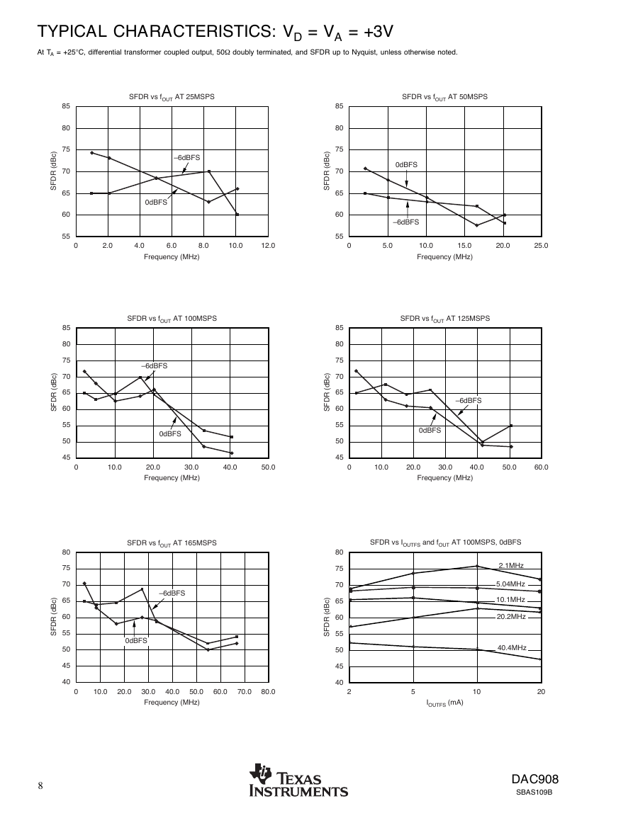
SFDR vs fOUT AT 25MSPS
–6dBFS
0dBFS
)
c
B
d
(
R
D
F
S
85
80
75
70
65
60
55
SFDR vs fOUT AT 50MSPS
0dBFS
–6dBFS
0
2.0
4.0
6.0
8.0
10.0
12.0
0
5.0
Frequency (MHz)
10.0
15.0
Frequency (MHz)
20.0
25.0
SFDR vs fOUT AT 100MSPS
–6dBFS
0dBFS
SFDR vs fOUT AT 125MSPS
–6dBFS
0dBFS
)
c
B
d
(
R
D
F
S
85
80
75
70
65
60
55
50
45
0
10.0
20.0
30.0
Frequency (MHz)
40.0
50.0
0
10.0
20.0
30.0
40.0
50.0
60.0
Frequency (MHz)
SFDR vs fOUT AT 165MSPS
–6dBFS
0dBFS
0
10.0
20.0
40.0
30.0
50.0
Frequency (MHz)
60.0
70.0
80.0
)
c
B
d
(
R
D
F
S
80
75
70
65
60
55
50
45
40
X
2
SFDR vs IOUTFS and fOUT AT 100MSPS, 0dBFS
2.1MHz
5.04MHz
10.1MHz
20.2MHz
X
40.4MHz
X
20
10
IOUTFS (mA)
X
5
DAC908
SBAS109B
�




 2023年江西萍乡中考道德与法治真题及答案.doc
 2012年重庆南川中考生物真题及答案.doc
 2013年江西师范大学地理学综合及文艺理论基础考研真题.doc
 2020年四川甘孜小升初语文真题及答案I卷.doc
 2020年注册岩土工程师专业基础考试真题及答案.doc
 2023-2024学年福建省厦门市九年级上学期数学月考试题及答案.doc
 2021-2022学年辽宁省沈阳市大东区九年级上学期语文期末试题及答案.doc
 2022-2023学年北京东城区初三第一学期物理期末试卷及答案.doc
 2018上半年江西教师资格初中地理学科知识与教学能力真题及答案.doc
 2012年河北国家公务员申论考试真题及答案-省级.doc
 2020-2021学年江苏省扬州市江都区邵樊片九年级上学期数学第一次质量检测试题及答案.doc
 2022下半年黑龙江教师资格证中学综合素质真题及答案.doc