Qualcomm Technologies, Inc.
MSM8996/APQ8096/MSM8996SG/APQ8096SG
Device Specification
80-NT204-1 Rev. P
February 9, 2016
For additional information or to submit technical questions go to https://createpoint.qti.qualcomm.com
Confidential and Proprietary – Qualcomm Technologies, Inc.
NO PUBLIC DISCLOSURE PERMITTED: Please report postings of this document on public servers or websites to:
DocCtrlAgent@qualcomm.com.
Restricted Distribution: Not to be distributed to anyone who is not an employee of either Qualcomm Technologies, Inc. or its affiliated
companies without the express approval of Qualcomm Configuration Management.
Not to be used, copied, reproduced, or modified in whole or in part, nor its contents revealed in any manner to others without the express
written permission of Qualcomm Technologies, Inc.
Fluence, MSM, Qualcomm Adreno, Qualcomm Secure Execution Environment, Qualcomm Hexagon, Qualcomm Kryo, Qualcomm RF360, and
Qualcomm Snapdragon are products of Qualcomm Technologies, Inc. Qualcomm IZat is a product of Qualcomm Atheros, Inc. Other
Qualcomm products referenced herein are products of Qualcomm Technologies, Inc. or its subsidiaries.
Adreno, Fluence, Hexagon, MSM, Qualcomm, Qualcomm RF360, and Snapdragon are trademarks of Qualcomm Incorporated, registered in
the United States and other countries. IZat and Kryo are trademarks of Qualcomm Incorporated. Other product and brand names may be
trademarks or registered trademarks of their respective owners.
This technical data may be subject to U.S. and international export, re-export, or transfer (“export”) laws. Diversion contrary to U.S. and
international law is strictly prohibited.
Qualcomm Technologies, Inc.
5775 Morehouse Drive
San Diego, CA 92121
U.S.A.
© 2014-2016 Qualcomm Technologies, Inc. All rights reserved.
�
Revision history
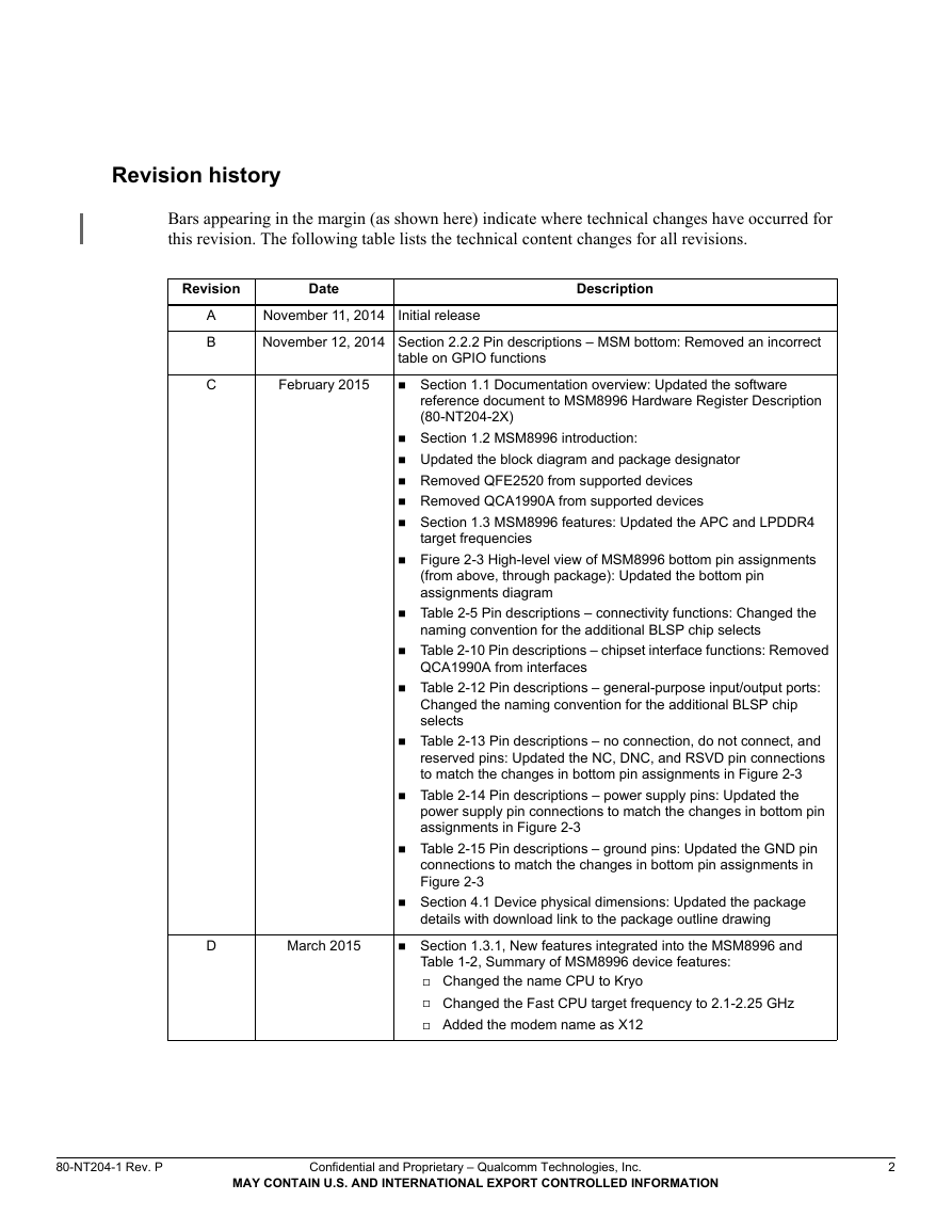
Bars appearing in the margin (as shown here) indicate where technical changes have occurred for
this revision. The following table lists the technical content changes for all revisions.
Revision
Date
Description
A
B
C
February 2015
November 11, 2014 Initial release
November 12, 2014 Section 2.2.2 Pin descriptions – MSM bottom: Removed an incorrect
table on GPIO functions
Section 1.1 Documentation overview: Updated the software
reference document to MSM8996 Hardware Register Description
(80-NT204-2X)
Section 1.2 MSM8996 introduction:
Updated the block diagram and package designator
Removed QFE2520 from supported devices
Removed QCA1990A from supported devices
Section 1.3 MSM8996 features: Updated the APC and LPDDR4
target frequencies
Figure 2-3 High-level view of MSM8996 bottom pin assignments
(from above, through package): Updated the bottom pin
assignments diagram
Table 2-5 Pin descriptions – connectivity functions: Changed the
naming convention for the additional BLSP chip selects
Table 2-10 Pin descriptions – chipset interface functions: Removed
QCA1990A from interfaces
Table 2-12 Pin descriptions – general-purpose input/output ports:
Changed the naming convention for the additional BLSP chip
selects
Table 2-13 Pin descriptions – no connection, do not connect, and
reserved pins: Updated the NC, DNC, and RSVD pin connections
to match the changes in bottom pin assignments in Figure 2-3
Table 2-14 Pin descriptions – power supply pins: Updated the
power supply pin connections to match the changes in bottom pin
assignments in Figure 2-3
Table 2-15 Pin descriptions – ground pins: Updated the GND pin
connections to match the changes in bottom pin assignments in
Figure 2-3
Section 4.1 Device physical dimensions: Updated the package
details with download link to the package outline drawing
Section 1.3.1, New features integrated into the MSM8996 and
Table 1-2, Summary of MSM8996 device features:
Changed the name CPU to Kryo
Changed the Fast CPU target frequency to 2.1-2.25 GHz
Added the modem name as X12
D
March 2015
80-NT204-1 Rev. P
Confidential and Proprietary – Qualcomm Technologies, Inc.
MAY CONTAIN U.S. AND INTERNATIONAL EXPORT CONTROLLED INFORMATION
2
�
MSM8996/APQ8096/MSM8996SG/APQ8096SG Device Specification
Revision history
Revision
D
(cont.)
Date
March 2015
E
June 2, 2015
Description
Figure 2-3, High-level view of MSM8996 bottom pin assignments
(from above, through package); Table 2-13, Pin descriptions – no
connection, do not connect, and reserved pins; Table 2-14, Pin
descriptions – power supply pins; Figure 2-6, High-level view of
MSM8996 top pin assignments (from above); Table 2-19, Pin
description – UFS memory:
Changed some DNC and RSVD pins to support UFS POP
(uPOP)
Added Section 3.2, Operating conditions
Figure 1-1 MSM8996 functional block diagram and example
application: Removed the UFS (optional) block and renamed eUFS
to UFS
Section 1.3.1 New features integrated into the MSM8996
Updated the Kryo core targets and Qualcomm Adreno GPU
speeds
Changed X12 modem support to LTE CAT12
Changed the DSI DPHY version to 1.2
Table 1-2 Summary of MSM8996 device features
Updated the Kryo core targets and Adreno GPU speeds
Updated the video and camera feature support
Changed the DSI DPHY version to 1.2
Table 1-3 Key X12 modem features: Updated the LTE category
feature description
Figure 2-3 Pin descriptions – memory support functions
Corrected the pin name for D26 to EBI_ZQ2
Changed UFS-POP related pin names to DNC as uPOP has
been defeatured
Corrected GPIO_9, GPIO_50, and GPIO_54 default pull state in
Table 2-5 Pin descriptions – connectivity functions, Table 2-7 Pin
descriptions – internal functions, Table 2-8 MSM8996 wakeup pins
for MSM power management (MPM), and Table 2-12 Pin
descriptions – general-purpose input/output ports
Table 2-12 Pin descriptions – general-purpose input/output ports:
Removed QSPI functions
Updated Figure 4-1 994C MNSP (15.6 × 15 × 0.69 mm) outline
drawing
Added content to the following sections or chapters for the first
time:
Section 3.3 Power distribution network through Section 3.11
Internal functions
Section 4.2 Part marking
Section 4.3 Device ordering information
Section 4.4 Device moisture sensitivity level
Section 4.5 Thermal characteristics
Chapter 5 Carrier, handling, and storage information
Chapter 6 PCB mounting guidelines
80-NT204-1 Rev. P
Confidential and Proprietary – Qualcomm Technologies, Inc.
MAY CONTAIN U.S. AND INTERNATIONAL EXPORT CONTROLLED INFORMATION
3
�
MSM8996/APQ8096/MSM8996SG/APQ8096SG Device Specification
Revision history
Revision
Date
F
June 5, 2015
G
July 2015
Description
Removed (Advance Information) from the document title
Figure 1-1, MSM8996 functional block diagram and example
application: changed the TD-HSPA to 256 QAM
Section 1.2, MSM8996 introduction:
Changed the TD-HSPA to 256 QAM
Updated LTE support to Cat 12 and data rates to 600 Mbps
download, 150 Mbps upload
Added reference to PoP requirement document 80-VP300-9
Added WTR3950 reference documents family number
Table 1-2, Summary of MSM8996 device features: Corrected DSI
DPHY to DPHY1.2 and VESA DSC to 1.1
Figure 2-3, High-level view of MSM8996 bottom pin assignments
(from above, through package): Corrected pad name for BF20 to
HDMI_REXT
Table 2-12, Pin descriptions – general-purpose input/output ports:
Added function and description PA_INDICATOR to GPIO_116
Figure 2-6, High-level view of MSM8996 top pin assignments (from
above): Changed uPOP pins on the top side to DNC
Table 2-17, Pin descriptions – no connection, do not connect, and
reserved pins: Added uPOP pins on the top side to DNC
Deleted Table 2-19 Pin Description – UFS Memory
Section 1.3.1 New features integrated into the MSM8996 and
Table 1-2 Summary of MSM8996 device features: Increased the
gold applications processor cluster target from 2.0 GHz to
2.15 GHz
Figure 2-3 High-level view of MSM8996 bottom pin assignments
(from above, through package): Corrected the pin name of pad
AM8 from PCIE0_REXT to PCIE_REXT
Table 3-4 MSM8996 PDN specifications – EBI: Split the maximum
impedance values to reflect both lumped and distributed DC and
added a footnote
Section 3.4 Power sequencing: Swapped steps 6 and 8
Figure 4-3 Device identification code and Table 4-2 Device
identification details: Corrected the feature code from AC to AB
Updated document links in the following locations:
Section 4.1 Device physical dimensions
Section 4.5 Thermal characteristics
80-NT204-1 Rev. P
Confidential and Proprietary – Qualcomm Technologies, Inc.
MAY CONTAIN U.S. AND INTERNATIONAL EXPORT CONTROLLED INFORMATION
4
�
MSM8996/APQ8096/MSM8996SG/APQ8096SG Device Specification
Revision history
Revision
Date
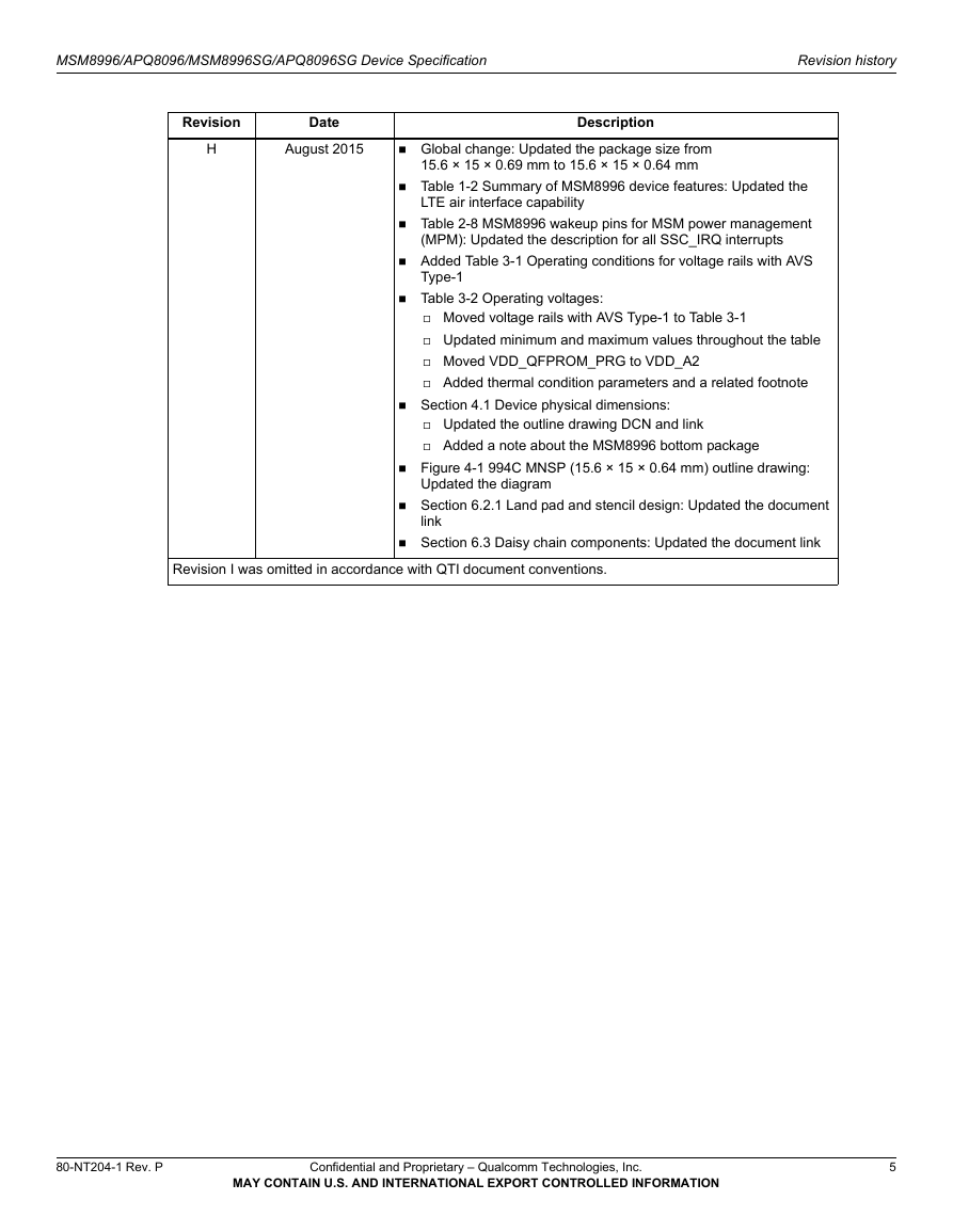
H
August 2015
Description
Global change: Updated the package size from
15.6 × 15 × 0.69 mm to 15.6 × 15 × 0.64 mm
Table 1-2 Summary of MSM8996 device features: Updated the
LTE air interface capability
Table 2-8 MSM8996 wakeup pins for MSM power management
(MPM): Updated the description for all SSC_IRQ interrupts
Added Table 3-1 Operating conditions for voltage rails with AVS
Type-1
Table 3-2 Operating voltages:
Moved voltage rails with AVS Type-1 to Table 3-1
Updated minimum and maximum values throughout the table
Moved VDD_QFPROM_PRG to VDD_A2
Added thermal condition parameters and a related footnote
Section 4.1 Device physical dimensions:
Updated the outline drawing DCN and link
Added a note about the MSM8996 bottom package
Figure 4-1 994C MNSP (15.6 × 15 × 0.64 mm) outline drawing:
Updated the diagram
Section 6.2.1 Land pad and stencil design: Updated the document
link
Section 6.3 Daisy chain components: Updated the document link
Revision I was omitted in accordance with QTI document conventions.
80-NT204-1 Rev. P
Confidential and Proprietary – Qualcomm Technologies, Inc.
MAY CONTAIN U.S. AND INTERNATIONAL EXPORT CONTROLLED INFORMATION
5
�
MSM8996/APQ8096/MSM8996SG/APQ8096SG Device Specification
Revision history
Revision
Date
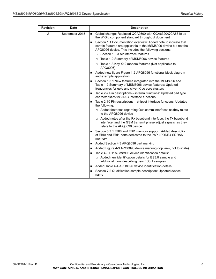
J
September 2015
Description
Global change: Replaced QCA9500 with QCA6320/QCA6310 as
the WiGig component standard throughout document
Section 1.1 Documentation overview: Added note to indicate that
certain features are applicable to the MSM8996 device but not the
APQ8096 device. This includes the following sections:
Section 1.3.3 Air interface features
Table 1-2 Summary of MSM8996 device features
Table 1-3 Key X12 modem features (Not applicable to
APQ8096)
Added new figure Figure 1-2 APQ8096 functional block diagram
and example application
Section 1.3.1 New features integrated into the MSM8996 and
Table 1-2 Summary of MSM8996 device features: Updated
frequencies for gold and silver Kryo core clusters
Table 2-7 Pin descriptions – internal functions: Updated pad type
characteristics for JTAG interface functions
Table 2-10 Pin descriptions – chipset interface functions: Updated
the following:
Added footnotes regarding Qualcomm interfaces as they relate
to the APQ8096 device
Added notes after the Rx baseband interface, the Tx baseband
interface, and the GSM transmit phase adjust signals, as they
relate to the APQ8096 device
Section 3.7.1 EBI0 and EBI1 memory support: Added description
of EBI0 and EBI1 ports dedicated to the PoP LPDDR4 SDRAM
memory
Added Section 4.3 APQ8096 part marking
Added Figure 4-3 APQ8096 device marking (top view, not to scale)
Table 4-3 P1: MSM8996 device identification details:
Added new identification details for ES3.0 sample and
additional rows describing new ES3.1 samples
Added Table 4-4 APQ8096 device identification details
Section 7.2 Qualification sample description: Updated device
name
80-NT204-1 Rev. P
Confidential and Proprietary – Qualcomm Technologies, Inc.
MAY CONTAIN U.S. AND INTERNATIONAL EXPORT CONTROLLED INFORMATION
6
�
MSM8996/APQ8096/MSM8996SG/APQ8096SG Device Specification
Revision history
Revision
Date
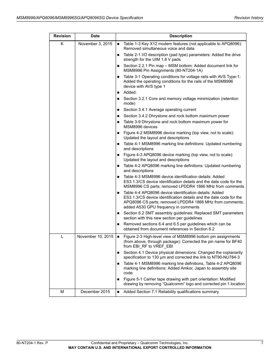
K
November 3, 2015
Description
Table 1-3 Key X12 modem features (not applicable to APQ8096):
Removed simultaneous voice and data
Table 2-1 I/O description (pad type) parameters: Added the drive
strength for the UIM 1.8 V pads
Section 2.2.1 Pin map – MSM bottom: Added document link for
MSM8996 Pin Assignments (80-NT204-1A)
Table 3-1 Operating conditions for voltage rails with AVS Type-1:
Added the operating conditions for the rails of the MSM8996
device with AVS type 1
Added:
Section 3.2.1 Core and memory voltage minimization (retention
mode)
Section 3.4.1 Average operating current
Section 3.4.2 Dhrystone and rock bottom maximum power
Table 3-9 Dhrystone and rock bottom maximum power for
MSM8996 devices
Figure 4-2 MSM8996 device marking (top view, not to scale):
Updated the layout and descriptions
Table 4-1 MSM8996 marking line definitions: Updated numbering
and descriptions
Figure 4-3 APQ8096 device marking (top view, not to scale):
Updated the layout and descriptions
Table 4-2 APQ8096 marking line definitions: Updated numbering
and descriptions
Table 4-3 MSM8996 device identification details: Added
ES3.1.3/CS device identification details and the date code for the
MSM8996 CS parts; removed LPDDR4 1866 MHz from comments
Table 4-4 APQ8096 device identification details: Added
ES3.1.3/CS device identification details and the date code for the
APQ8096 CS parts; removed LPDDR4 1866 MHz from comments;
added A530 GPU frequency in comments
Section 6.2 SMT assembly guidelines: Replaced SMT parameters
section with this new section per guidelines
Removed sections 6.4 and 6.5 per guidelines which can be
obtained from document references in Section 6.2
L
November 10, 2015 Figure 2-3 High-level view of MSM8996 bottom pin assignments
(from above, through package): Corrected the pin name for BF40
from EBI_RF to VREF_EBI
Section 4.1 Device physical dimensions: Changed the coplanarity
specification to 130 µm and corrected the link to NT90-NU784-3
Table 4-1 MSM8996 marking line definitions, Table 4-2 APQ8096
marking line definitions: Added Amkor, Japan to assembly site
code
Figure 5-1 Carrier tape drawing with part orientation: Modified
drawing by removing “Qualcomm” logo and corrected pin 1 location
M
December 2015
Added Section 7.1 Reliability qualifications summary
80-NT204-1 Rev. P
Confidential and Proprietary – Qualcomm Technologies, Inc.
MAY CONTAIN U.S. AND INTERNATIONAL EXPORT CONTROLLED INFORMATION
7
�
MSM8996/APQ8096/MSM8996SG/APQ8096SG Device Specification
Revision history
Revision
Date
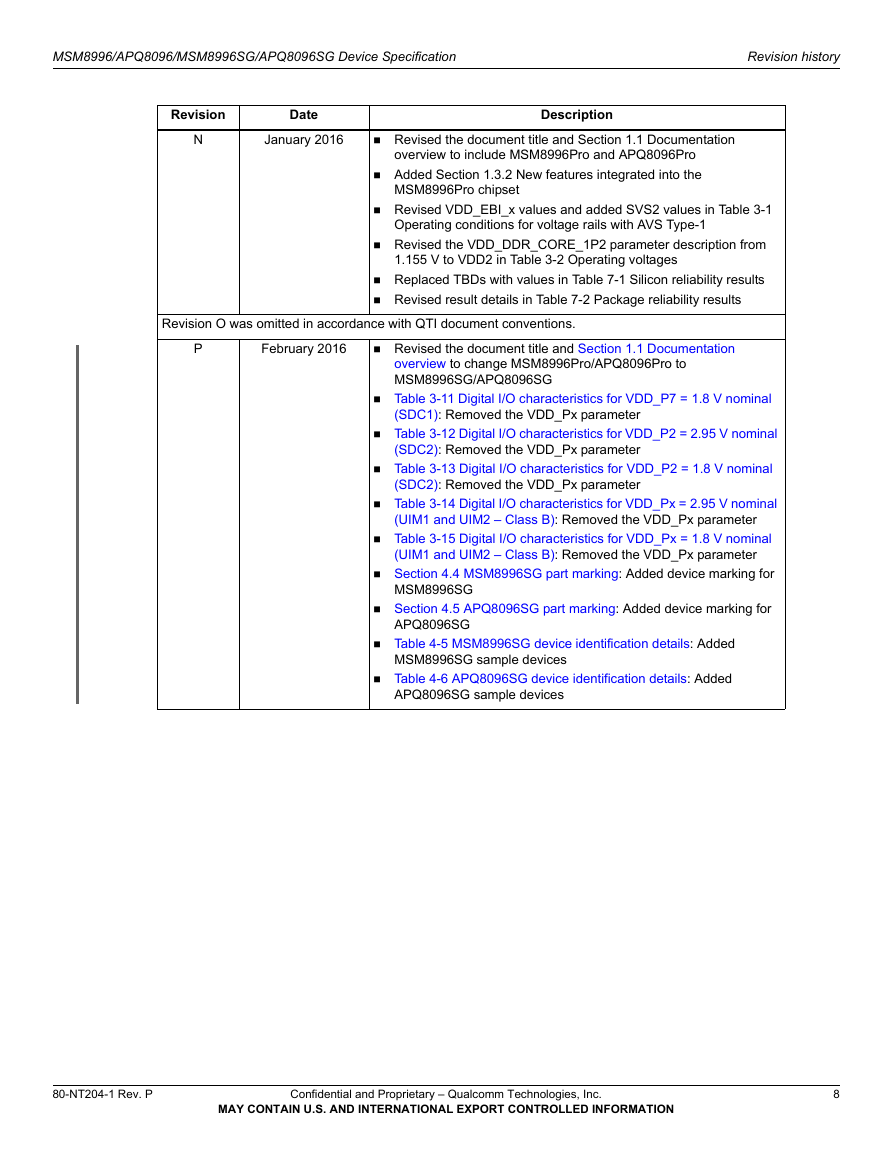
N
January 2016
Description
Revised the document title and Section 1.1 Documentation
overview to include MSM8996Pro and APQ8096Pro
Added Section 1.3.2 New features integrated into the
MSM8996Pro chipset
Revised VDD_EBI_x values and added SVS2 values in Table 3-1
Operating conditions for voltage rails with AVS Type-1
Revised the VDD_DDR_CORE_1P2 parameter description from
1.155 V to VDD2 in Table 3-2 Operating voltages
Replaced TBDs with values in Table 7-1 Silicon reliability results
Revised result details in Table 7-2 Package reliability results
Revision O was omitted in accordance with QTI document conventions.
P
February 2016
Revised the document title and Section 1.1 Documentation
overview to change MSM8996Pro/APQ8096Pro to
MSM8996SG/APQ8096SG
Table 3-11 Digital I/O characteristics for VDD_P7 = 1.8 V nominal
(SDC1): Removed the VDD_Px parameter
Table 3-12 Digital I/O characteristics for VDD_P2 = 2.95 V nominal
(SDC2): Removed the VDD_Px parameter
Table 3-13 Digital I/O characteristics for VDD_P2 = 1.8 V nominal
(SDC2): Removed the VDD_Px parameter
Table 3-14 Digital I/O characteristics for VDD_Px = 2.95 V nominal
(UIM1 and UIM2 – Class B): Removed the VDD_Px parameter
Table 3-15 Digital I/O characteristics for VDD_Px = 1.8 V nominal
(UIM1 and UIM2 – Class B): Removed the VDD_Px parameter
Section 4.4 MSM8996SG part marking: Added device marking for
MSM8996SG
Section 4.5 APQ8096SG part marking: Added device marking for
APQ8096SG
Table 4-5 MSM8996SG device identification details: Added
MSM8996SG sample devices
Table 4-6 APQ8096SG device identification details: Added
APQ8096SG sample devices
80-NT204-1 Rev. P
Confidential and Proprietary – Qualcomm Technologies, Inc.
MAY CONTAIN U.S. AND INTERNATIONAL EXPORT CONTROLLED INFORMATION
8
�


 2023年江西萍乡中考道德与法治真题及答案.doc
 2012年重庆南川中考生物真题及答案.doc
 2013年江西师范大学地理学综合及文艺理论基础考研真题.doc
 2020年四川甘孜小升初语文真题及答案I卷.doc
 2020年注册岩土工程师专业基础考试真题及答案.doc
 2023-2024学年福建省厦门市九年级上学期数学月考试题及答案.doc
 2021-2022学年辽宁省沈阳市大东区九年级上学期语文期末试题及答案.doc
 2022-2023学年北京东城区初三第一学期物理期末试卷及答案.doc
 2018上半年江西教师资格初中地理学科知识与教学能力真题及答案.doc
 2012年河北国家公务员申论考试真题及答案-省级.doc
 2020-2021学年江苏省扬州市江都区邵樊片九年级上学期数学第一次质量检测试题及答案.doc
 2022下半年黑龙江教师资格证中学综合素质真题及答案.doc