TI Information — Selective Disclosure
TCAN4550-Q1 CAN FD Controller with Integrated Transceiver
TCAN4550-Q1
SLLSEZ5 –JANUARY 2018
1 Features
1• AEC Q100: Qualified for Automotive Applications
– Device Temperature: –40°C to 125°C Ambient
– Device HBM Classification Level H2: ±8000 V
– Device CDM Classification Level C5: ±750 V
• Standalone CAN FD Controller with Integrated
CAN Transceiver and Serial Peripheral Interface
(SPI)
• CAN FD Controller Supports both ISO 11898-
1:2015 and Bosch M-CAN Revision 3.2.1.1
• Meets the Requirements of ISO 11898-2:2016
• CAN FD Data Rates up to 5 Mbps with up to 20
MHz SPI Clock Speed
• Classic CAN Backwards Compatible
• Operating Modes:
– Normal Mode:
– CAN FD Communication up to 5 Mbps
– Low Power Standby Mode
– Low Power Sleep Mode
3.3 V to 5 V MCU Support
•
• Wide Operating Ranges
– ±42 V Bus Fault Protection
– ±12 V Common Mode
• Optimized Behavior when Unpowered
– Bus and Logic Terminals are High Impedance
(No Load to Operating Bus or Application)
– Power Up and Down Glitch Free Operation
• Expanded Bus Fault Detection and Reporting
Industrial Transportation
Infotainment and Cluster
2 Applications
• Body Electronics and Lighting
•
• Passive Safety
•
3 Description
The TCAN4550-Q1 is a CAN FD controller with
integrated CAN (Control Area Network) transceiver
supporting data rates up to 5 Mbps. The device
interfaces with a microprocessor using SPI
. The
CAN FD processor meets the specifications of the
ISO11898-1:2015 standard and the CAN transceiver
meets the specifications of the ISO11898-2:2016 high
speed CAN physical layer standard. The TCAN4550-
Q1 can wake up via local wake up from a state
change on the WAKE pin or by the CAN bus
implementing the ISO Wake Up Pattern (WUP).
The device includes many protection features
providing device and network robustness.
Device Information(1)
PART NUMBER
BODY SIZE (NOM)
TCAN4550-Q1
4.50 mm x 3.50 mm
(1) For all available packages, see the orderable addendum at
PACKAGE
VQFN (20)
the end of the data sheet.
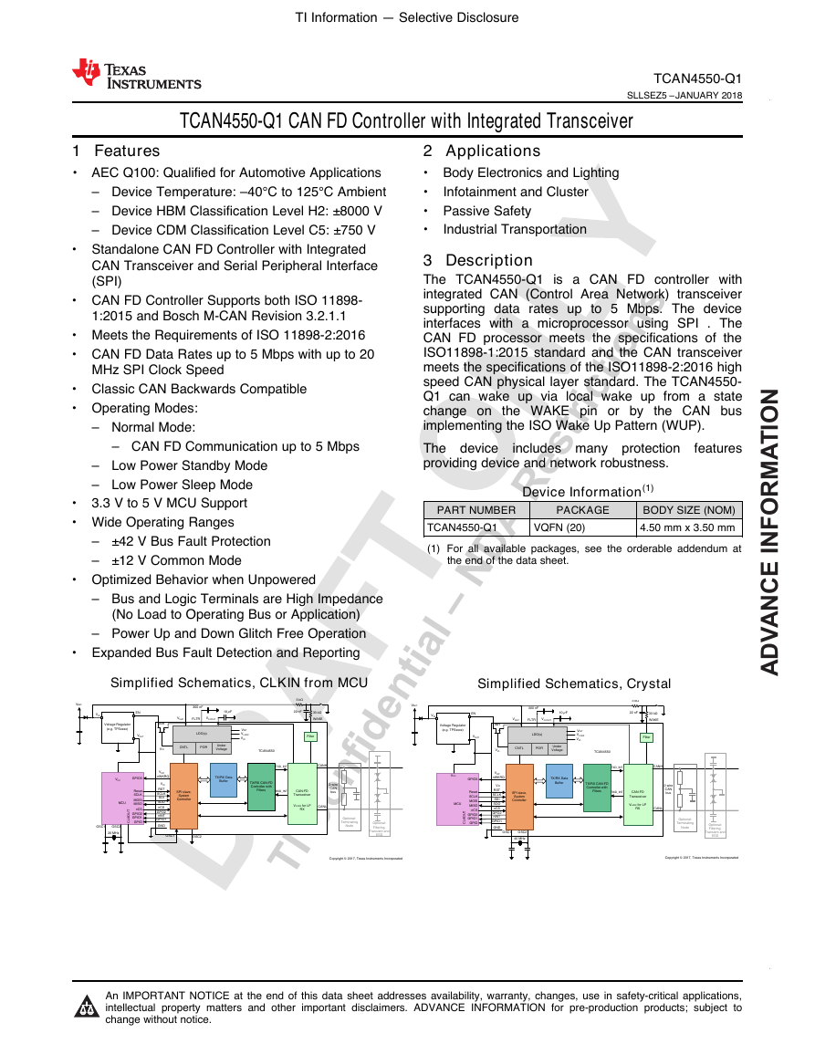
Simplified Schematics, CLKIN from MCU
Simplified Schematics, Crystal
1
An IMPORTANT NOTICE at the end of this data sheet addresses availability, warranty, changes, use in safety-critical applications,
intellectual property matters and other important disclaimers. ADVANCE INFORMATION for pre-production products; subject to
change without notice.
TI Confidential–NDARestrictionsADVANCE INFORMATIONSCLKGPIO1ResetMCUVCCGPIOOptional:TerminatingNodeOptional: Filtering, Transient and ESDVoltage Regulator(e.g. TPSxxxx)VINVOUTVBATMOSIMISOnCSVCCINT1VLVRX for LP RX2-wire CAN busSCLKTX/RX CAN-FD Controller with FiltersTX/RX Data BufferCANHTXD_INTRXD_INTLDO(s)Under VoltagePOROSC1OSC2RSTVIOGNDFilterVSUPVINTCNTLVLVRXVCCINT2CANLVIOVIOnCSnINTCAN-FD TransceiverVLVRX for LP RXGPIO1INHENSPI slave, System Controller GPIO2GPO2SDOSDInWKRQGPIO3VINTVCCOUTFLTR300 nF 10 µF TCAN4550OSC1OSC220 MHzCLKOUTCopyright © 2017, Texas Instruments IncorporatedWAKE22 nF 33 k3 kSCLKGPIO1ResetMCUVCCGPIOOptional:TerminatingNodeOptional: Filtering, Transient and ESDVoltage Regulator(e.g. TPSxxxx)VINVOUTVBATMOSIMISOnCSVCCINT1VLVRX for LP RX2-wire CAN busSCLKTX/RX CAN-FD Controller with FiltersTX/RX Data BufferCANHTXD_INTRXD_INTLDO(s)Under VoltagePORRSTVIOGNDFilterVSUPVINTCNTLVLVRXVCCINT2CANLVIOVIOnCSnINTCAN-FD TransceiverVLVRX for LP RXGPIO1INHENSPI slave, System Controller GPIO2GPO2SDOSDInWKRQGPIO3VINTVCCOUTFLTR300 nF 10 µF TCAN4550OSC1OSC240 MHzCLKOUTCopyright © 2017, Texas Instruments IncorporatedWAKE22 nF 33 k3 k�
TI Information — Selective Disclosure
TCAN4550-Q1
SLLSEZ5 –JANUARY 2018
Table of Contents
www.ti.com
1
Features.................................................................. 1
2 Applications ........................................................... 1
3 Description ............................................................. 1
4 Revision History..................................................... 2
5 Pin Configuration and Functions ......................... 3
6 Specifications......................................................... 4
6.1 Absolute Maximum Ratings ...................................... 4
6.2 ESD Ratings.............................................................. 4
6.3 ESD Ratings, IC Specification .................................. 4
6.4 Recommended Operating Conditions....................... 5
6.5 Thermal Information.................................................. 5
6.6 Supply Characteristics .............................................. 5
6.7 Electrical Characteristics........................................... 6
6.8 Timing Requirements................................................ 9
6.9 Switching Characteristics.......................................... 9
7 Parameter Measurement Information ................ 11
8 Detailed Description ............................................ 23
8.1 Overview ................................................................. 23
8.2 Functional Block Diagram ....................................... 24
8.3 Feature Description................................................. 27
8.4 Device Functional Modes........................................ 29
8.5 Programming .......................................................... 45
8.6 Register Maps......................................................... 48
9 Application and Implementation ...................... 145
9.1 Application Information.......................................... 145
9.2 Typical Application ............................................... 148
10 Power Supply Recommendations ................... 150
11 Layout................................................................. 151
11.1 Layout Guidelines ............................................... 151
11.2 Layout Example .................................................. 152
12 Device and Documentation Support ............... 153
12.1 Documentation Support ..................................... 153
12.2 Receiving Notification of Documentation
Updates.................................................................. 153
12.3 Community Resources........................................ 153
12.4 Trademarks ......................................................... 153
12.5 Electrostatic Discharge Caution.......................... 154
12.6 Glossary .............................................................. 154
13 Mechanical, Packaging, and Orderable
Information ......................................................... 154
4 Revision History
NOTE: Page numbers for previous revisions may differ from page numbers in the current version.
DATE
September 2017
REVISION
*
NOTES
Initial release.
2
Submit Documentation Feedback
Copyright © 2018, Texas Instruments Incorporated
Product Folder Links: TCAN4550-Q1
TI Confidential–NDARestrictionsADVANCE INFORMATION�
TI Information — Selective Disclosure
www.ti.com
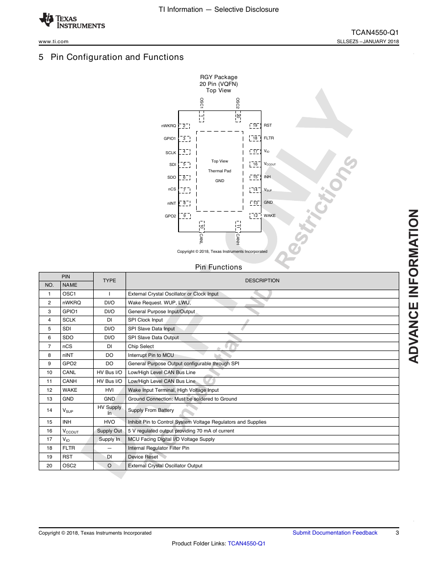
5 Pin Configuration and Functions
RGY Package
20 Pin (VQFN)
Top View
TCAN4550-Q1
SLLSEZ5 –JANUARY 2018
PIN
NAME
OSC1
nWKRQ
GPIO1
SCLK
SDI
SDO
nCS
nINT
GPO2
CANL
CANH
WAKE
GND
VSUP
INH
VCCOUT
VIO
FLTR
RST
OSC2
NO.
1
2
3
4
5
6
7
8
9
10
11
12
13
14
15
16
17
18
19
20
Pin Functions
DESCRIPTION
External Crystal Oscillator or Clock Input
Wake Request. WUP, LWU,
General Purpose Input/Output
SPI Clock Input
SPI Slave Data Input
SPI Slave Data Output
Chip Select
Interrupt Pin to MCU
General Purpose Output configurable through SPI
TYPE
I
DI/O
DI/O
DI
DI/O
DI/O
DI
DO
DO
HV Bus I/O Low/High Level CAN Bus Line
HV Bus I/O Low/High Level CAN Bus Line
HVI
GND
Wake Input Terminal, High Voltage Input
Ground Connection: Must be soldered to Ground
HV Supply
In
HVO
Supply From Battery
Inhibit Pin to Control System Voltage Regulators and Supplies
5 V regulated output providing 70 mA of current
Supply Out
Supply In MCU Facing Digital I/O Voltage Supply
—
DI
O
Internal Regulator Filter Pin
Device Reset
External Crystal Oscillator Output
Copyright © 2018, Texas Instruments Incorporated
Submit Documentation Feedback
3
Product Folder Links: TCAN4550-Q1
TI Confidential–NDARestrictionsADVANCE INFORMATIONTop ViewThermal PadGND234567CANHCANLOSC2OSC1SCLKSDISDOWAKEVSUP1201110191817161514VIOINHGNDnINTnCSGPIO1891312VCCOUTGPO2nWKRQFLTRRSTCopyright © 2018, Texas Instruments Incorporated�
www.ti.com
UNIT
MAX
42
6
6
42
42
MIN
–0.3
–0.3
–0.3
–42
–0.3
–0.3
–0.3
–0.5
TI Information — Selective Disclosure
TCAN4550-Q1
SLLSEZ5 –JANUARY 2018
6 Specifications
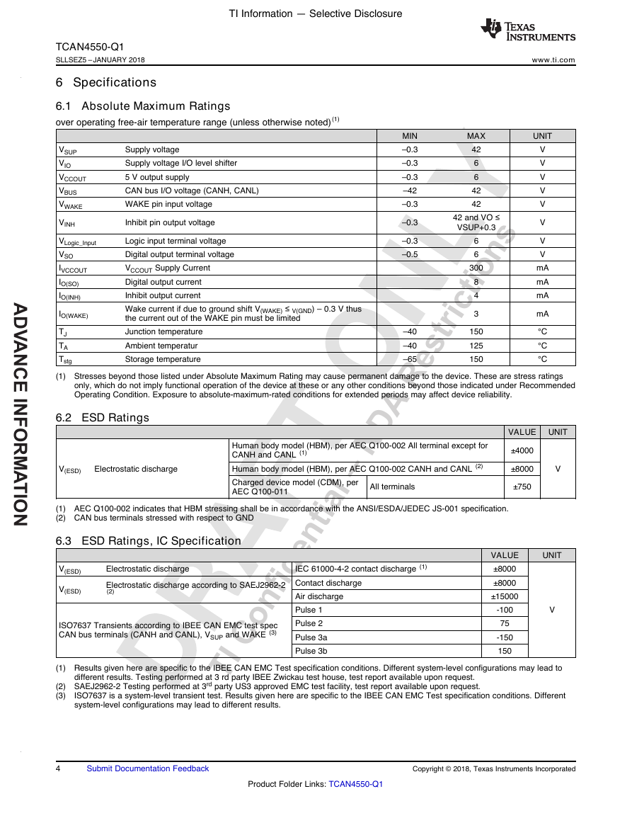
6.1 Absolute Maximum Ratings
over operating free-air temperature range (unless otherwise noted)(1)
Inhibit pin output voltage
Supply voltage
Supply voltage I/O level shifter
5 V output supply
CAN bus I/O voltage (CANH, CANL)
WAKE pin input voltage
VSUP
VIO
VCCOUT
VBUS
VWAKE
VINH
VLogic_Input
VSO
IVCCOUT
IO(SO)
IO(INH)
IO(WAKE)
TJ
TA
Tstg
(1) Stresses beyond those listed under Absolute Maximum Rating may cause permanent damage to the device. These are stress ratings
Logic input terminal voltage
Digital output terminal voltage
VCCOUT Supply Current
Digital output current
Inhibit output current
Wake current if due to ground shift V(WAKE) ≤ V(GND) – 0.3 V thus
the current out of the WAKE pin must be limited
Junction temperature
Ambient temperatur
Storage temperature
42 and VO ≤
VSUP+0.3
V
V
mA
mA
mA
mA
6
6
300
8
4
–40
–40
–65
3
150
125
150
V
V
V
V
V
V
°C
°C
°C
only, which do not imply functional operation of the device at these or any other conditions beyond those indicated under Recommended
Operating Condition. Exposure to absolute-maximum-rated conditions for extended periods may affect device reliability.
6.2 ESD Ratings
V(ESD)
Electrostatic discharge
Human body model (HBM), per AEC Q100-002 All terminal except for
CANH and CANL (1)
Human body model (HBM), per AEC Q100-002 CANH and CANL (2)
Charged device model (CDM), per
AEC Q100-011
All terminals
VALUE
UNIT
±4000
±8000
±750
V
(1) AEC Q100-002 indicates that HBM stressing shall be in accordance with the ANSI/ESDA/JEDEC JS-001 specification.
(2) CAN bus terminals stressed with respect to GND
6.3 ESD Ratings, IC Specification
V(ESD)
V(ESD)
Electrostatic discharge
Electrostatic discharge according to SAEJ2962-2
(2)
ISO7637 Transients according to IBEE CAN EMC test spec
CAN bus terminals (CANH and CANL), VSUP and WAKE (3)
IEC 61000-4-2 contact discharge (1)
Contact discharge
Air discharge
Pulse 1
Pulse 2
Pulse 3a
Pulse 3b
UNIT
V
VALUE
±8000
±8000
±15000
-100
75
-150
150
(1) Results given here are specific to the IBEE CAN EMC Test specification conditions. Different system-level configurations may lead to
different results. Testing performed at 3 rd party IBEE Zwickau test house, test report available upon request.
(2) SAEJ2962-2 Testing performed at 3rd party US3 approved EMC test facility, test report available upon request.
(3)
ISO7637 is a system-level transient test. Results given here are specific to the IBEE CAN EMC Test specification conditions. Different
system-level configurations may lead to different results.
4
Submit Documentation Feedback
Copyright © 2018, Texas Instruments Incorporated
Product Folder Links: TCAN4550-Q1
TI Confidential–NDARestrictionsADVANCE INFORMATION�
TI Information — Selective Disclosure
www.ti.com
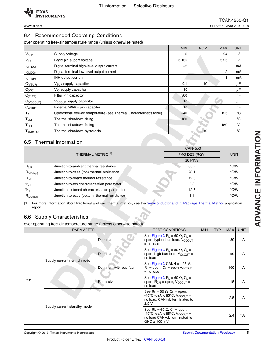
6.4 Recommended Operating Conditions
over operating free-air temperature range (unless otherwise noted)
VSUP
VIO
IOH(DO)
IOL(DO)
IO (INH)
C(VSUP)
C(VIO)
C(FLTR)
C(VCCOUT)
CWAKE
TA
TSDR
TSDF
TSD(HYS)
Supply voltage
Logic pin supply voltage
Digital terminal high-level output current
Digital terminal low-level output current
INH output current
VSUP supply capacitor
VIO supply capacitor
Filter Pin capacitor
VCCOUT supply capacitor
External WAKE pin capacitor
Operational free-air temperature (see Thermal Characteristics table)
Thermal shutdown rising
Thermal shutdown falling
Thermal shutdown hysteresis
6.5 Thermal Information
THERMAL METRIC(1)
TCAN4550-Q1
SLLSEZ5 –JANUARY 2018
MIN
6
3.135
–2
0.1
10
300
10
10
–40
160
NOM
10
10
MAX
24
5.25
2
1
125
150
UNIT
V
V
mA
mA
mA
µF
µF
nF
µF
nF
°C
℃
℃
℃
TCAN4550
PKG DES (RGY)
20 PINS
UNIT
RθJA
RθJC(top)
RθJB
ΨJT
ΨJB
RθJC(bot)
(1) For more information about traditional and new thermal metrics, see the Semiconductor and IC Package Thermal Metrics application
Junction-to-ambient thermal resistance
Junction-to-case (top) thermal resistance
Junction-to-board thermal resistance
Junction-to-top characterization parameter
Junction-to-board characterization parameter
Junction-to-case (bottom) thermal resistance
35.2
28.1
12.8
0.3
12.7
1.1
°C/W
°C/W
°C/W
°C/W
°C/W
°C/W
report.
6.6 Supply Characteristics
over operating free-air temperature range (unless otherwise noted)
PARAMETER
TEST CONDITIONS
MIN
TYP MAX UNIT
Supply current normal mode
Isup
Supply current standby mode
Dominant
Dominant
Dominant with bus fault
Recessive
See Figure 3 RL = 60 Ω, CL =
open. typical bus load. VCCOUT
= no load
See Figure 3 RL = 50 Ω, CL =
open, high bus load. VCCOUT =
no load
See Figure 3 CANH = - 25 V,
RL = open, CL = open VCCOUT
= no load
See Figure 3 RL = 60 Ω, CL =
open, RCM = open, VCCOUT =
no load
See RL = 60 Ω, CL = open,
-40°C < TA < 85°C, VCCOUT =
no load, CANH/L terminated to
2.5 V
See RL = 60 Ω, CL = open,
-40°C < TA < 85°C, VCCOUT =
no load CANH/L terminated to
GND ± 100 mV
80 mA
90 mA
100 mA
15 mA
2.5 mA
2.4 mA
Copyright © 2018, Texas Instruments Incorporated
Submit Documentation Feedback
5
Product Folder Links: TCAN4550-Q1
TI Confidential–NDARestrictionsADVANCE INFORMATION�
TI Information — Selective Disclosure
TCAN4550-Q1
SLLSEZ5 –JANUARY 2018
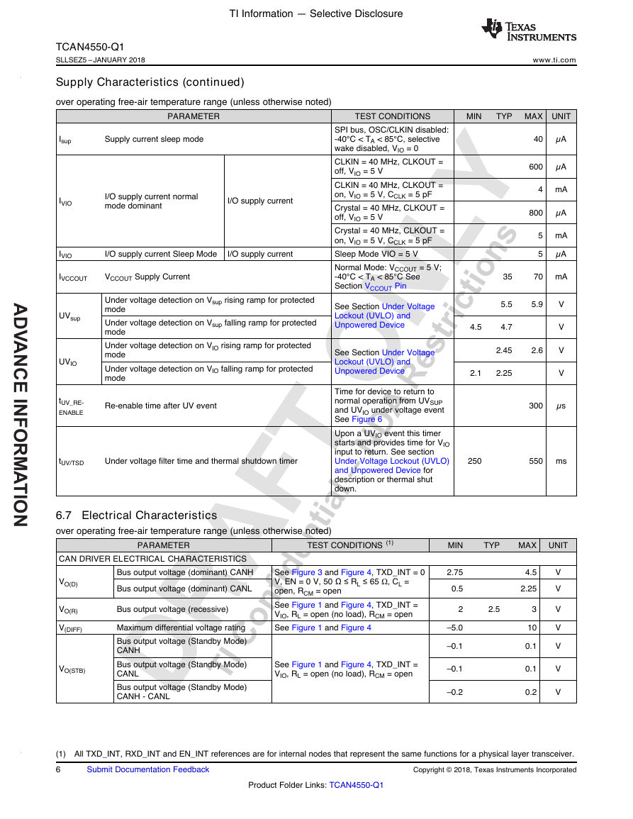
Supply Characteristics (continued)
over operating free-air temperature range (unless otherwise noted)
www.ti.com
PARAMETER
TEST CONDITIONS
MIN
TYP MAX UNIT
Isup
Supply current sleep mode
IVIO
IVIO
I/O supply current normal
mode dominant
I/O supply current
I/O supply current Sleep Mode
I/O supply current
IVCCOUT
VCCOUT Supply Current
Under voltage detection on Vsup rising ramp for protected
mode
Under voltage detection on Vsup falling ramp for protected
mode
Under voltage detection on VIO rising ramp for protected
mode
Under voltage detection on VIO falling ramp for protected
mode
Re-enable time after UV event
UVsup
UVIO
tUV_RE-
ENABLE
tUV/TSD
Under voltage filter time and thermal shutdown timer
SPI bus, OSC/CLKIN disabled:
-40°C < TA < 85°C, selective
wake disabled, VIO = 0
CLKIN = 40 MHz, CLKOUT =
off, VIO = 5 V
CLKIN = 40 MHz, CLKOUT =
on, VIO = 5 V, CCLK = 5 pF
Crystal = 40 MHz, CLKOUT =
off, VIO = 5 V
Crystal = 40 MHz, CLKOUT =
on, VIO = 5 V, CCLK = 5 pF
Sleep Mode VIO = 5 V
Normal Mode: VCCOUT = 5 V;
-40°C < TA < 85°C See
Section VCCOUT Pin
See Section Under Voltage
Lockout (UVLO) and
Unpowered Device
See Section Under Voltage
Lockout (UVLO) and
Unpowered Device
Time for device to return to
normal operation from UVSUP
and UVIO under voltage event
See Figure 6
Upon a UVIO event this timer
starts and provides time for VIO
input to return. See section
Under Voltage Lockout (UVLO)
and Unpowered Device for
description or thermal shut
down.
40
µA
600
µA
4 mA
800
µA
5 mA
5
µA
70 mA
5.9
V
V
V
V
35
5.5
4.7
4.5
2.45
2.6
2.1
2.25
300
µs
250
550 ms
6.7 Electrical Characteristics
over operating free-air temperature range (unless otherwise noted)
PARAMETER
TEST CONDITIONS (1)
MIN
TYP
MAX UNIT
CAN DRIVER ELECTRICAL CHARACTERISTICS
VO(D)
VO(R)
V(DIFF)
VO(STB)
Bus output voltage (dominant) CANH
Bus output voltage (dominant) CANL
Bus output voltage (recessive)
Maximum differential voltage rating
Bus output voltage (Standby Mode)
CANH
Bus output voltage (Standby Mode)
CANL
Bus output voltage (Standby Mode)
CANH - CANL
See Figure 3 and Figure 4, TXD_INT = 0
V, EN = 0 V, 50 Ω ≤ RL ≤ 65 Ω, CL =
open, RCM = open
See Figure 1 and Figure 4, TXD_INT =
VIO, RL = open (no load), RCM = open
See Figure 1 and Figure 4
See Figure 1 and Figure 4, TXD_INT =
VIO, RL = open (no load), RCM = open
2.75
0.5
2
–5.0
–0.1
–0.1
–0.2
2.5
4.5
2.25
3
10
0.1
0.1
0.2
V
V
V
V
V
V
V
(1) All TXD_INT, RXD_INT and EN_INT references are for internal nodes that represent the same functions for a physical layer transceiver.
6
Copyright © 2018, Texas Instruments Incorporated
Submit Documentation Feedback
Product Folder Links: TCAN4550-Q1
TI Confidential–NDARestrictionsADVANCE INFORMATION�
TI Information — Selective Disclosure
www.ti.com
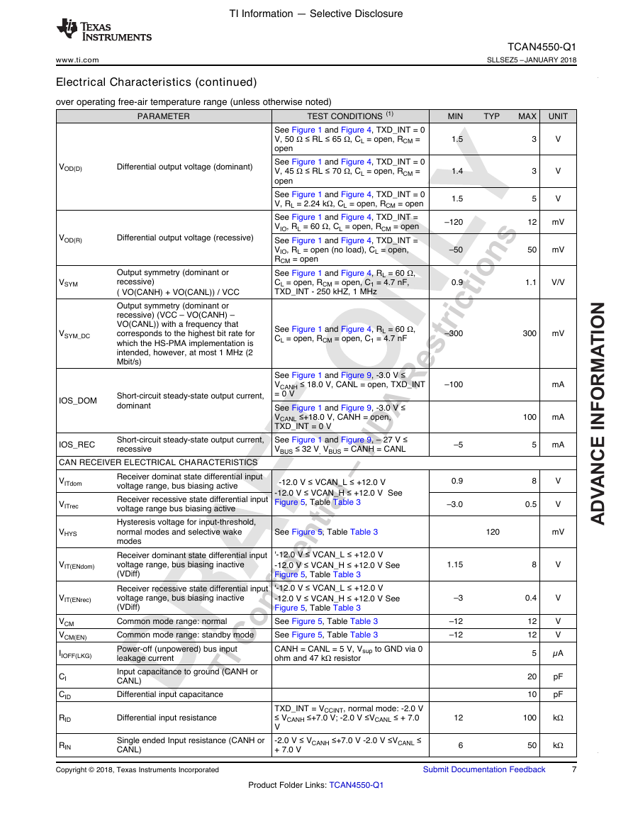
Electrical Characteristics (continued)
over operating free-air temperature range (unless otherwise noted)
TCAN4550-Q1
SLLSEZ5 –JANUARY 2018
TYP
MAX UNIT
3
3
5
12
50
V
V
V
mV
mV
1.1
V/V
TEST CONDITIONS (1)
See Figure 1 and Figure 4, TXD_INT = 0
V, 50 Ω ≤ RL ≤ 65 Ω, CL = open, RCM =
open
See Figure 1 and Figure 4, TXD_INT = 0
V, 45 Ω ≤ RL ≤ 70 Ω, CL = open, RCM =
open
See Figure 1 and Figure 4, TXD_INT = 0
V, RL = 2.24 kΩ, CL = open, RCM = open
See Figure 1 and Figure 4, TXD_INT =
VIO, RL = 60 Ω, CL = open, RCM = open
See Figure 1 and Figure 4, TXD_INT =
VIO, RL = open (no load), CL = open,
RCM = open
See Figure 1 and Figure 4, RL = 60 Ω,
CL = open, RCM = open, C1 = 4.7 nF,
TXD_INT - 250 kHZ, 1 MHz
MIN
1.5
1.4
1.5
–120
–50
0.9
See Figure 1 and Figure 4, RL = 60 Ω,
CL = open, RCM = open, C1 = 4.7 nF
–300
300
mV
PARAMETER
VOD(D)
Differential output voltage (dominant)
VOD(R)
Differential output voltage (recessive)
VSYM
VSYM_DC
Output symmetry (dominant or
recessive)
( VO(CANH) + VO(CANL)) / VCC
Output symmetry (dominant or
recessive) (VCC – VO(CANH) –
VO(CANL)) with a frequency that
corresponds to the highest bit rate for
which the HS-PMA implementation is
intended, however, at most 1 MHz (2
Mbit/s)
IOS_DOM
Short-circuit steady-state output current,
dominant
IOS_REC
Short-circuit steady-state output current,
recessive
VIT(ENdom)
CAN RECEIVER ELECTRICAL CHARACTERISTICS
Receiver dominat state differential input
voltage range, bus biasing active
Receiver recessive state differential input
voltage range bus biasing active
Hysteresis voltage for input-threshold,
normal modes and selective wake
modes
Receiver dominant state differential input
voltage range, bus biasing inactive
(VDiff)
Receiver recessive state differential input
voltage range, bus biasing inactive
(VDiff)
Common mode range: normal
Common mode range: standby mode
Power-off (unpowered) bus input
leakage current
Input capacitance to ground (CANH or
CANL)
Differential input capacitance
VCM
VCM(EN)
IIOFF(LKG)
VIT(ENrec)
VITdom
VITrec
VHYS
CI
CID
See Figure 1 and Figure 9, -3.0 V ≤
VCANH ≤ 18.0 V, CANL = open, TXD_INT
= 0 V
See Figure 1 and Figure 9, -3.0 V ≤
VCANL ≤+18.0 V, CANH = open,
TXD_INT = 0 V
See Figure 1 and Figure 9, – 27 V ≤
VBUS ≤ 32 V, VBUS = CANH = CANL
-12.0 V ≤ VCAN_L ≤ +12.0 V
-12.0 V ≤ VCAN_H ≤ +12.0 V See
Figure 5, Table Table 3
See Figure 5, Table Table 3
'-12.0 V ≤ VCAN_L ≤ +12.0 V
-12.0 V ≤ VCAN_H ≤ +12.0 V See
Figure 5, Table Table 3
'-12.0 V ≤ VCAN_L ≤ +12.0 V
-12.0 V ≤ VCAN_H ≤ +12.0 V See
Figure 5, Table Table 3
See Figure 5, Table Table 3
See Figure 5, Table Table 3
CANH = CANL = 5 V, Vsup to GND via 0
ohm and 47 kΩ resistor
–100
mA
100
mA
120
–5
0.9
–3.0
1.15
–3
–12
–12
12
6
5
8
0.5
8
0.4
12
12
5
20
10
100
50
mA
V
V
mV
V
V
V
V
µA
pF
pF
kΩ
kΩ
RID
RIN
Differential input resistance
Single ended Input resistance (CANH or
CANL)
TXD_INT = VCCINT, normal mode: -2.0 V
≤ VCANH ≤+7.0 V; -2.0 V ≤VCANL ≤ + 7.0
V
-2.0 V ≤ VCANH ≤+7.0 V -2.0 V ≤VCANL ≤
+ 7.0 V
Copyright © 2018, Texas Instruments Incorporated
Submit Documentation Feedback
7
Product Folder Links: TCAN4550-Q1
TI Confidential–NDARestrictionsADVANCE INFORMATION�
TI Information — Selective Disclosure
TCAN4550-Q1
SLLSEZ5 –JANUARY 2018
Electrical Characteristics (continued)
over operating free-air temperature range (unless otherwise noted)
PARAMETER
TEST CONDITIONS (1)
Input resistance matching: [1 –
(RIN(CANH) / (RIN(CANL))] × 100%
RIN(M)
VCCOUT SUPPLY TERMINAL
VCCOUT
5 V output supply
VDROP
Drop out voltage
ΔVCC(ΔVSUP)
Line regulation
Load regulation
Under voltage on VCCOUT
ΔVCC(ΔVSUPL)
UVCCOUT
FLTR TERMINAL
VMEASURE
C(FLTR)
INH OUTPUT TERMINAL (HIGH VOLTAGE OUTPUT)
High-level voltage drop INH with respect
to VSUP
Leakage current
ΔVH
ILKG(INH)
WAKE INPUT TERMINAL (HIGH VOLTAGE INPUT)
Voltage measured at FLTR pin
Filter pin capacitor
VIH
VIL
IIH
IIL
High-level input voltage
Low-level input voltage
High-level input current
Low-level input current
tWAKE
WAKE hold time
SDI, SCK, GPIO1 INPUT TERMINALS
VIH
High-level input voltage
Low-level input voltage
VIL
High-level input leakage current
IIH
Low-level input leakage current
IIL
CIN
Input Capacitance
Unpowered leakage current (SDI and
ILKG(OFF)
SCK Only)
nCS INPUT TERMINAL
VIH
VIL
IIH
IIL
ILKG(OFF)
RST INPUT TERMINAL
VIH
VIL
IIH
IIL
ILKG(OFF)
HIGH level input voltage
LOW level input voltage
HIGH level input leakage current
LOW level input leakage current
Unpowered leakage current
high-level input voltage
Low-level input voltage
high-level input leakage current
Low-level input leakage current
Unpowered leakage current
VCANH = VCANL = 5.0 V
ICCOUT = -100 mA to 0 mA; VSUP = 6 V
to 18 V; -40°C < TA < 85°C
VCCOUT = 5 V, VSUP = 12 V, ICCOUT =
100 mA
VSUP = 6 V to 24 V, ΔVCCOUT, ICCOUT =
10 mA
VSUP ≥ 6 V, ,ICCOUT = 1 mA to 100
mA, ΔVCCOUT, –40℃ ≤ TA ≤ 125℃
External filter capacitor
IINH = - 0.5 mA
INH = 0 V, Sleep Mode
Selective wake-up or standby mode,
WAKE pin enabled
Selective wake-up or standby mode,
WAKE pin enabled
WAKE = VSUP–1 V
WAKE = 1 V
Wake up time from a wake edge on
WAKE; standby, selective wake or sleep
mode
Inputs = VIO = 5.25 V
Inputs = 0 V, VIO = 0 V
TBD, at 20 MHz
Inputs = 5.25 V, VIO = VSUP = 0 V
nCS = VIO = 5.25 V
nCS = VIO = 0 V
nCS = 5.25 V, VIO = VSUP = 0 V
RST = VIO = 5.25 V
RST = 0 V
RST = VIO, VSUP = 0 V
www.ti.com
MIN
–1
TYP
MAX UNIT
1
%
4.75
5
5.25
V
300
500
15
20
4.2
4.55
1.5
300
0.5
–15
15
10
0
0
0
0
0
1
0.5
VSUP–3
25
50
0.3
1
–5
1
0.3
1
–5
1
0.3
10
1
1
mV
mV
mV
V
V
nF
V
µA
V
V
µA
µA
µs
VIO
VIO
µA
µA
pF
µA
VIO
VIO
µA
µA
µA
VIO
VIO
µA
µA
µA
–0.5
VSUP–2
–25
5
0.7
–1
–100
–1
0.7
–1
–50
–1
0.7
1
–1
–1
8
Submit Documentation Feedback
Copyright © 2018, Texas Instruments Incorporated
Product Folder Links: TCAN4550-Q1
TI Confidential–NDARestrictionsADVANCE INFORMATION�


 2023年江西萍乡中考道德与法治真题及答案.doc
 2012年重庆南川中考生物真题及答案.doc
 2013年江西师范大学地理学综合及文艺理论基础考研真题.doc
 2020年四川甘孜小升初语文真题及答案I卷.doc
 2020年注册岩土工程师专业基础考试真题及答案.doc
 2023-2024学年福建省厦门市九年级上学期数学月考试题及答案.doc
 2021-2022学年辽宁省沈阳市大东区九年级上学期语文期末试题及答案.doc
 2022-2023学年北京东城区初三第一学期物理期末试卷及答案.doc
 2018上半年江西教师资格初中地理学科知识与教学能力真题及答案.doc
 2012年河北国家公务员申论考试真题及答案-省级.doc
 2020-2021学年江苏省扬州市江都区邵樊片九年级上学期数学第一次质量检测试题及答案.doc
 2022下半年黑龙江教师资格证中学综合素质真题及答案.doc