www.ti.com
SLLS933D –NOVEMBER 2008–REVISED APRIL 2010
3.3-V CAN TRANSCEIVER
Check for Samples: SN65HVD233-HT
SN65HVD233-HT
1FEATURES
2• Bus-Pin Fault Protection Exceeds ±36 V
• Bus-Pin ESD Protection Exceeds 16-kV Human
Body Model (HBM)
• Compatible With ISO 11898
• Signaling Rates(1) up to 1 Mbps
• Extended –7-V to 12-V Common-Mode Range
• High-Input Impedance Allows for 120 Nodes
• LVTTL I/Os Are 5-V Tolerant
• Adjustable Driver Transition Times for
Improved Signal Quality
• Unpowered Node Does Not Disturb the Bus
• Low-Current Standby Mode . . . 200 mA Typical
• Power-Up/Down Glitch-Free Bus Inputs and
Outputs
– High Input Impedance With Low VCC
– Monolithic Output During Power Cycling
• Loopback for Diagnostic Functions Available
• DeviceNet™ Vendor ID #806
(1)
The signaling rate of a line is the number of voltage
transitions that are made per second expressed in the units
bps (bits per second).
APPLICATIONS
• Down-Hole Drilling
• High Temperature Environments
•
Industrial Automation
– DeviceNet™ Data Buses
– Smart Distributed Systems (SDS™)
• SAE J1939 Data Bus Interface
• NMEA 2000 Data Bus Interface
•
• CAN Data Bus Interface
ISO 11783 Data Bus Interface
XXX
SUPPORTS EXTREME TEMPERATURE
APPLICATIONS
• Controlled Baseline
• One Assembly/Test Site
• One Fabrication Site
• Available in Extreme (–55°C/210°C)
Temperature Range (1)
• Extended Product Life Cycle
• Extended Product-Change Notification
• Product Traceability
• Texas Instruments high temperature products
utilize highly optimized silicon (die) solutions
with design and process enhancements to
maximize performance over extended
temperatures.
area
network
(CAN)
operation
in
controller
DESCRIPTION/ORDERING INFORMATION
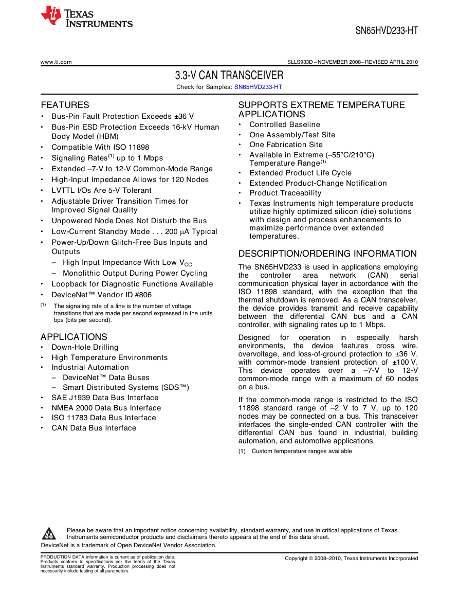
The SN65HVD233 is used in applications employing
the
serial
communication physical layer in accordance with the
ISO 11898 standard, with the exception that
the
thermal shutdown is removed. As a CAN transceiver,
the device provides transmit and receive capability
between the differential CAN bus and a CAN
controller, with signaling rates up to 1 Mbps.
harsh
Designed
especially
for
environments,
cross wire,
overvoltage, and loss-of-ground protection to ±36 V,
with common-mode transient protection of ±100 V.
This device operates over a –7-V to 12-V
common-mode range with a maximum of 60 nodes
on a bus.
If the common-mode range is restricted to the ISO
11898 standard range of –2 V to 7 V, up to 120
nodes may be connected on a bus. This transceiver
interfaces the single-ended CAN controller with the
differential CAN bus found in industrial, building
automation, and automotive applications.
(1) Custom temperature ranges available
the device features
1
Please be aware that an important notice concerning availability, standard warranty, and use in critical applications of Texas
Instruments semiconductor products and disclaimers thereto appears at the end of this data sheet.
2DeviceNet is a trademark of Open DeviceNet Vendor Association.
PRODUCTION DATA information is current as of publication date.
Products conform to specifications per the terms of
the Texas
Instruments standard warranty. Production processing does not
necessarily include testing of all parameters.
Copyright © 2008–2010, Texas Instruments Incorporated
�
SN65HVD233-HT
SLLS933D –NOVEMBER 2008–REVISED APRIL 2010
www.ti.com
This integrated circuit can be damaged by ESD. Texas Instruments recommends that all
appropriate precautions. Failure to observe proper handling and installation procedures can cause damage.
integrated circuits be handled with
ESD damage can range from subtle performance degradation to complete device failure. Precision integrated circuits may be more
susceptible to damage because very small parametric changes could cause the device not to meet its published specifications.
DESCRIPTION/ORDERING INFORMATION (CONTINUED)
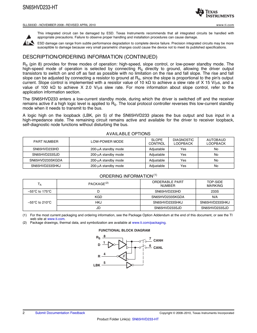
RS (pin 8) provides for three modes of operation: high-speed, slope control, or low-power standby mode. The
high-speed mode of operation is selected by connecting RS directly to ground, allowing the driver output
transistors to switch on and off as fast as possible with no limitation on the rise and fall slope. The rise and fall
slope can be adjusted by connecting a resistor to ground at RS, since the slope is proportional to the pin's output
current. Slope control is implemented with a resistor value of 10 kΩ to achieve a slew rate of Ⅹ 15 V/ms, and a
value of 100 kΩ to achieve Ⅹ 2.0 V/ms slew rate. For more information about slope control, refer to the
application information section.
The SN65HVD233 enters a low-current standby mode, during which the driver is switched off and the receiver
remains active if a high logic level is applied to RS. The local protocol controller reverses this low-current standby
mode when it needs to transmit to the bus.
A logic high on the loopback (LBK, pin 5) of the SN65HVD233 places the bus output and bus input in a
high-impedance state. The remaining circuit remains active and available for the driver to receiver loopback,
self-diagnostic node functions without disturbing the bus.
PART NUMBER
SN65HVD233HD
SN65HVD233SJD
SN65HVD233SKGDA
SN65HVD233SHKJ
TA
–55°C to 175°C
–55°C to 210°C
AVAILABLE OPTIONS
LOW-POWER MODE
200-mA standby mode
200-mA standby mode
200-mA standby mode
200-mA standby mode
SLOPE
CONTROL
Adjustable
Adjustable
Adjustable
Adjustable
DIAGNOSTIC
LOOPBACK
AUTOBAUD
LOOPBACK
Yes
Yes
Yes
Yes
No
No
No
No
ORDERING INFORMATION(1)
PACKAGE(2)
D
KGD
HKJ
JD
ORDERABLE PART
NUMBER
SN65HVD233HD
SN65HVD233SKGDA
SN65HVD233SHKJ
SN65HVD233SJD
TOP-SIDE
MARKING
233S
N/A
SN65HVD233SHKJ
SN65HVD233SJD
(1) For the most current packaging and ordering information, see the Package Option Addendum at the end of this document, or see the TI
web site at www.ti.com.
(2) Package drawings, thermal data, and symbolization are available at www.ti.com/packaging.
2
Submit Documentation Feedback
Copyright © 2008–2010, Texas Instruments Incorporated
Product Folder Link(s): SN65HVD233-HT
8145RSDRLBK76CANHCANLFUNCTIONAL BLOCK DIAGRAM�
SN65HVD233-HT
www.ti.com
SLLS933D –NOVEMBER 2008–REVISED APRIL 2010
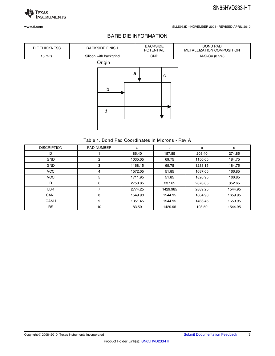
BARE DIE INFORMATION
DIE THICKNESS
BACKSIDE FINISH
15 mils.
Silicon with backgrind
BACKSIDE
POTENTIAL
GND
BOND PAD
METALLIZATION COMPOSITION
Al-Si-Cu (0.5%)
Table 1. Bond Pad Coordinates in Microns - Rev A
DISCRIPTION
PAD NUMBER
D
GND
GND
VCC
VCC
R
LBK
CANL
CANH
RS
1
2
3
4
5
6
7
8
9
10
a
86.40
1035.05
1168.15
1572.05
1711.95
2758.85
2774.25
1549.90
1351.45
83.50
b
157.85
69.75
69.75
51.85
51.85
237.65
1429.985
1544.95
1544.95
1429.95
c
203.40
1150.05
1283.15
1687.05
1826.95
2873.85
2889.25
1664.90
1466.45
198.50
d
274.85
184.75
184.75
166.85
166.85
352.65
1544.95
1659.95
1659.95
1544.95
Copyright © 2008–2010, Texas Instruments Incorporated
Submit Documentation Feedback
3
Product Folder Link(s): SN65HVD233-HT
abcdOrigin�
SN65HVD233-HT
SLLS933D –NOVEMBER 2008–REVISED APRIL 2010
www.ti.com
4
Submit Documentation Feedback
Copyright © 2008–2010, Texas Instruments Incorporated
Product Folder Link(s): SN65HVD233-HT
�
www.ti.com
SLLS933D –NOVEMBER 2008–REVISED APRIL 2010
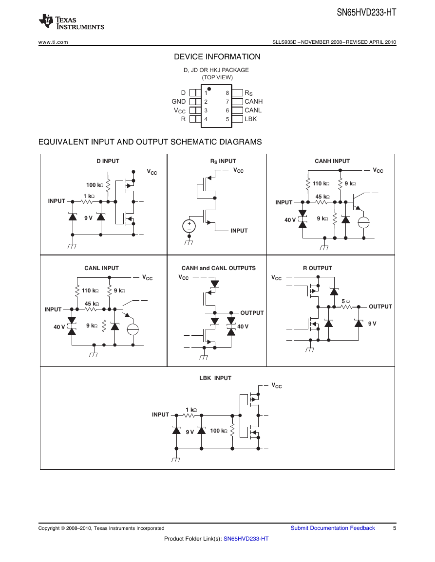
DEVICE INFORMATION
SN65HVD233-HT
EQUIVALENT INPUT AND OUTPUT SCHEMATIC DIAGRAMS
Copyright © 2008–2010, Texas Instruments Incorporated
Submit Documentation Feedback
5
Product Folder Link(s): SN65HVD233-HT
12348765DGNDVCCRRSCANHCANLLBKD, JD OR HKJ PACKAGE(TOPVIEW)1 kΩVCCINPUT9VD INPUT100 kΩ9 kΩ45 kΩ40VVCCCANH INPUT_+VCCINPUTRSINPUTINPUT9 kΩ110 kΩ9 kΩ45 kΩ40VVCCCANL INPUTINPUT9 kΩ110 kΩVCCCANH and CANL OUTPUTSOUTPUT40V5ΩVCCOUTPUT9VR OUTPUT1 kΩVCCINPUT9VLBK INPUT100 kΩ�
SN65HVD233-HT
SLLS933D –NOVEMBER 2008–REVISED APRIL 2010
www.ti.com
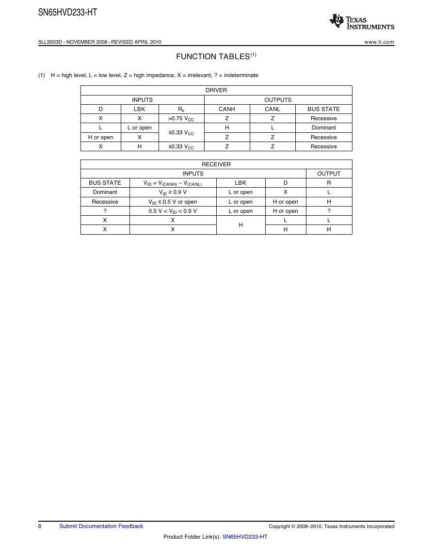
(1) H = high level, L = low level, Z = high impedance, X = irrelevant, ? = indeterminate
FUNCTION TABLES(1)
D
X
L
INPUTS
LBK
X
L or open
H or open
X
X
H
Rs
>0.75 VCC
≤0.33 VCC
≤0.33 VCC
DRIVER
CANH
Z
H
Z
Z
RECEIVER
BUS STATE
Dominant
Recessive
?
X
X
INPUTS
VID = V(CANH) – V(CANL)
VID ≥ 0.9 V
VID ≤ 0.5 V or open
0.5 V < VID < 0.9 V
X
X
OUTPUTS
CANL
Z
L
Z
Z
BUS STATE
Recessive
Dominant
Recessive
Recessive
OUTPUT
LBK
L or open
L or open
L or open
H
D
X
H or open
H or open
L
H
R
L
H
?
L
H
6
Submit Documentation Feedback
Copyright © 2008–2010, Texas Instruments Incorporated
Product Folder Link(s): SN65HVD233-HT
�
SN65HVD233-HT
www.ti.com
SLLS933D –NOVEMBER 2008–REVISED APRIL 2010
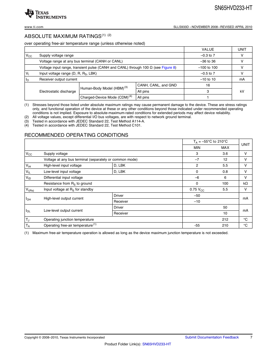
ABSOLUTE MAXIMUM RATINGS(1) (2)
over operating free-air temperature range (unless otherwise noted)
VCC
VI
IO
Supply voltage range
Voltage range at any bus terminal (CANH or CANL)
Voltage input range, transient pulse (CANH and CANL) through 100 Ω (see Figure 8)
Input voltage range (D, R, RS, LBK)
Receiver output current
Electrostatic discharge
Human-Body Model (HBM) (3)
Charged-Device Mode (CDM) (4)
CANH, CANL, and GND
All pins
All pins
VALUE
–0.3 to 7
–36 to 36
–100 to 100
–0.5 to 7
–10 to 10
16
3
1
UNIT
V
V
V
V
mA
kV
(1) Stresses beyond those listed under absolute maximum ratings may cause permanent damage to the device. These are stress ratings
only, and functional operation of the device at these or any other conditions beyond those indicated under recommended operating
conditions is not implied. Exposure to absolute-maximum-rated conditions for extended periods may affect device reliability.
(2) All voltage values, except differential I/O bus voltages, are with respect to network ground terminal.
(3) Tested in accordance with JEDEC Standard 22, Test Method A114-A.
(4) Tested in accordance with JEDEC Standard 22, Test Method C101.
RECOMMENDED OPERATING CONDITIONS
VCC
VIH
VIL
VID
VI(Rs)
IOH
IOL
TJ
TA
Supply voltage
Voltage at any bus terminal (separately or common mode)
High-level input voltage
Low-level input voltage
Differential input voltage
Resistance from RS to ground
Input voltage at RS for standby
D, LBK
D, LBK
High-level output current
Low-level output current
Operating junction temperature
Operating free-air temperature (1)
Driver
Receiver
Driver
Receiver
TA = –55°C to 210°C
MIN
MAX
3.6
12
5.5
0.8
6
100
5.5
3
–7
2
0
–6
0
0.75 VCC
–50
–10
-55
50
10
212
210
UNIT
V
V
V
V
V
kΩ
V
mA
mA
°C
°C
(1) Maximum free-air temperature operation is allowed as long as the device maximum junction temperature is not exceeded.
Copyright © 2008–2010, Texas Instruments Incorporated
Submit Documentation Feedback
7
Product Folder Link(s): SN65HVD233-HT
�
SN65HVD233-HT
SLLS933D –NOVEMBER 2008–REVISED APRIL 2010
www.ti.com
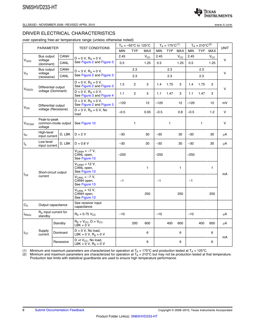
DRIVER ELECTRICAL CHARACTERISTICS
over operating free-air temperature range (unless otherwise noted)
PARAMETER
TEST CONDITIONS
VO(D)
VO
Bus output
voltage
(dominant)
Bus output
voltage
(recessive)
CANH
CANL
CANH
CANL
VOD(D)
Differential output
voltage (Dominant)
VOD
Differential output
voltage (Recessive)
D = 0 V, RS = 0 V,
See Figure 2 and Figure 3
D = 3 V, RS = 0 V,
See Figure 2 and Figure 3
D = 0 V, RS = 0 V,
See Figure 2 and Figure 3
D = 0 V, RS = 0 V,
See Figure 3 and Figure 4
D = 3 V, RS = 0 V,
See Figure 2 and Figure 3
D = 3 V, RS = 0 V, No
load
VOC(pp)
IIH
IIL
Peak-to-peak
common-mode output See Figure 10
voltage
High-level
input current
Low-level
input current
D, LBK D = 0.8 V
D, LBK D = 2 V
VCANH = –7 V,
CANL open,
See Figure 13
VCANH = 12 V,
CANL open,
See Figure 13
VCANL = –7 V,
CANH open,
See Figure 13
VCANL = 12 V,
CANH open,
See Figure 13
See receiver input
capacitance
IOS
Short-circuit output
current
CO
IIRs(s)
Output capacitance
RS input current for
standby
TA = –55°C to 125°C
MIN
2.45
TYP
TA = 175°C(1)
TA = 210°C(2)
MAX MIN TYP MAX MIN TYP MAX
VCC
VCC
1.25
1.25
VCC
1.25
2.45
0.5
2.45
0.5
0.5
1.5
1.1
–120
–0.5
–30
–30
–250
2.3
2.3
2
2
1
2.3
2.3
2.3
2.3
3
3
1.4
1.75
1.1
1.47
3
3
1.4
1.75
1.1
1.47
12
–120
12
–120
0.05
–0.5
0.8
–0.5
1
1
–30
–30
–250
30
30
1
–30
–30
–250
30
30
1
3
3
12
1.2
30
30
1
–1
–1
–1
250
250
250
UNIT
V
V
V
mV
V
V
mA
mA
mA
mA
mA
mA
RS = 0.75 VCC
–10
–10
–10
ICC
Supply
current
Standby
Dominant
Recessive
RS = VCC, D = VCC,
LBK = 0 V
D = 0 V, No load,
LBK = 0 V, RS = 0 V
D =t VCC, No load,
LBK = 0 V, RS = 0 V
200
600
400
600
400
600
6
6
6
6
6
6
(1) Minimum and maximum parameters are characterized for operation at TA = 175°C and production tested at TA = 125°C.
(2) Minimum and maximum parameters are characterized for operation at TA = 210°C but may not be production tested at that temperature.
Production test limits with statistical guardbands are used to ensure high temperature performance.
8
Submit Documentation Feedback
Copyright © 2008–2010, Texas Instruments Incorporated
Product Folder Link(s): SN65HVD233-HT
�



 2023年江西萍乡中考道德与法治真题及答案.doc
 2012年重庆南川中考生物真题及答案.doc
 2013年江西师范大学地理学综合及文艺理论基础考研真题.doc
 2020年四川甘孜小升初语文真题及答案I卷.doc
 2020年注册岩土工程师专业基础考试真题及答案.doc
 2023-2024学年福建省厦门市九年级上学期数学月考试题及答案.doc
 2021-2022学年辽宁省沈阳市大东区九年级上学期语文期末试题及答案.doc
 2022-2023学年北京东城区初三第一学期物理期末试卷及答案.doc
 2018上半年江西教师资格初中地理学科知识与教学能力真题及答案.doc
 2012年河北国家公务员申论考试真题及答案-省级.doc
 2020-2021学年江苏省扬州市江都区邵樊片九年级上学期数学第一次质量检测试题及答案.doc
 2022下半年黑龙江教师资格证中学综合素质真题及答案.doc