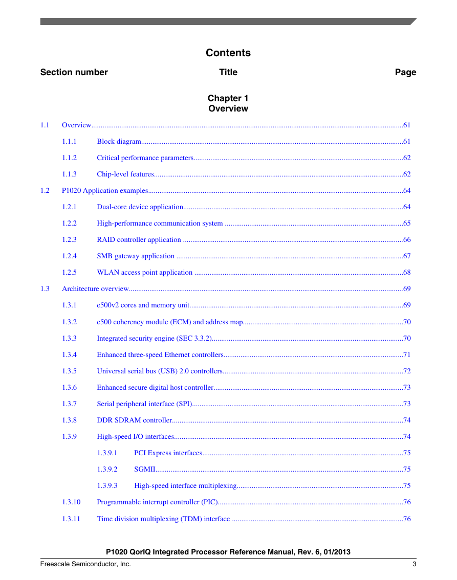
Chapter 1: Overview
Overview
Block diagram
Critical performance parameters
Chip-level features
P1020 Application examples
Dual-core device application
High-performance communication system
RAID controller application
SMB gateway application
WLAN access point application
Architecture overview
e500v2 cores and memory unit
e500 coherency module (ECM) and address map
Integrated security engine (SEC 3.3.2)
Enhanced three-speed Ethernet controllers
Universal serial bus (USB) 2.0 controllers
Enhanced secure digital host controller
Serial peripheral interface (SPI)
DDR SDRAM controller
High-speed I/O interfaces
PCI Express interfaces
SGMII
High-speed interface multiplexing
Programmable interrupt controller (PIC)
Time division multiplexing (TDM) interface
DMA, I2C, DUART, and enhanced local bus controller
Device boot locations
Boot sequencer
System performance monitor
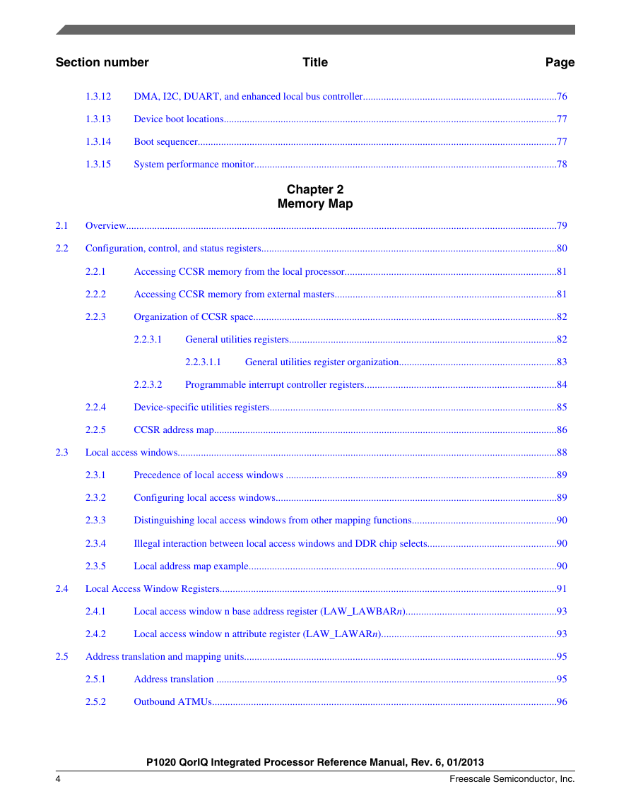
Chapter 2: Memory Map
Overview
Configuration, control, and status registers
Accessing CCSR memory from the local processor
Accessing CCSR memory from external masters
Organization of CCSR space
General utilities registers
General utilities register organization
Programmable interrupt controller registers
Device-specific utilities registers
CCSR address map
Local access windows
Precedence of local access windows
Configuring local access windows
Distinguishing local access windows from other mapping functions
Illegal interaction between local access windows and DDR chip selects
Local address map example
Local Access Window Registers
LAW
LAW_LAWBARn
LAW_LAWARn
Address translation and mapping units
Address translation
Outbound ATMUs
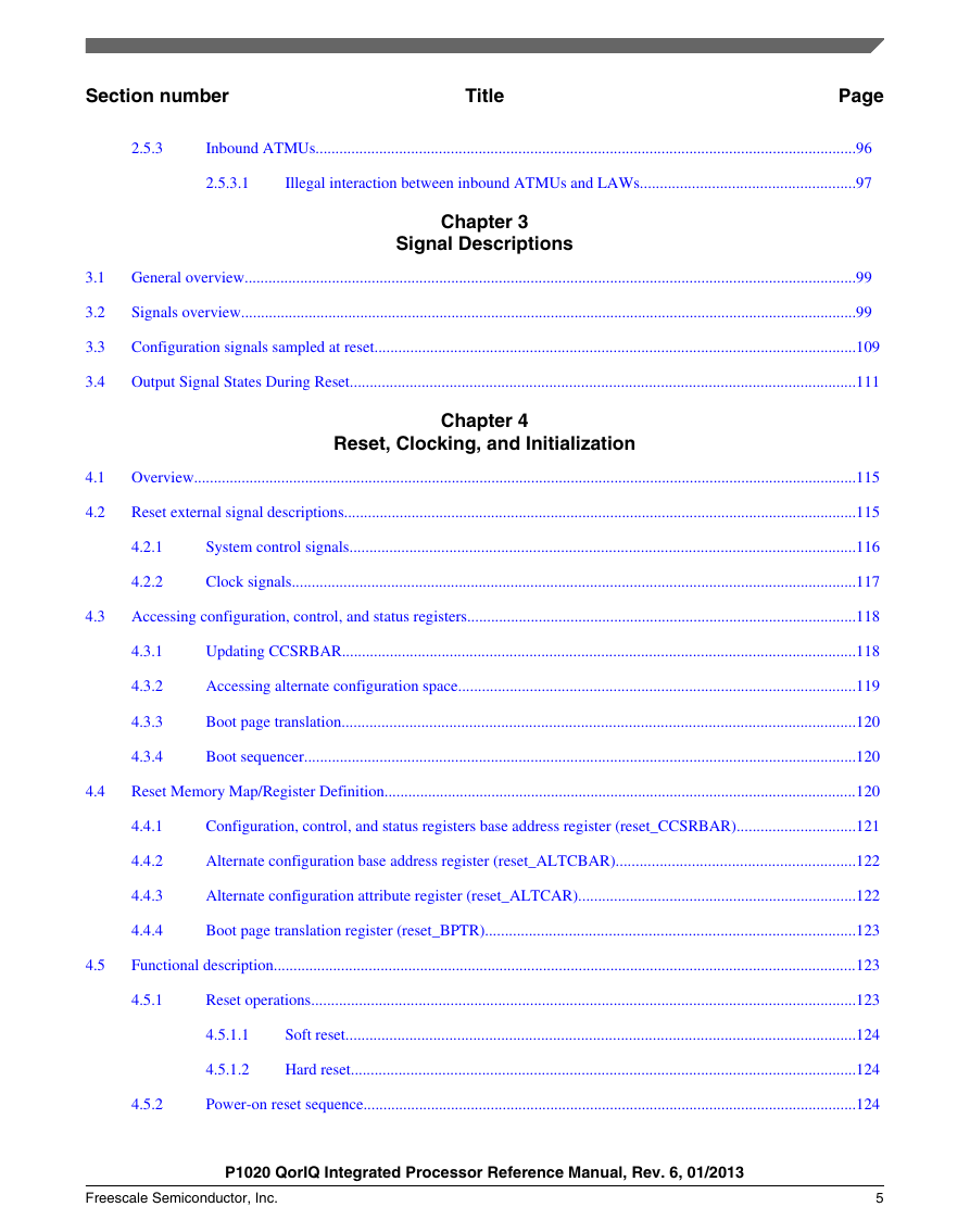
Inbound ATMUs
Illegal interaction between inbound ATMUs and LAWs
Chapter 3: Signal Descriptions
General overview
Signals overview
Configuration signals sampled at reset
Output Signal States During Reset
Chapter 4: Reset, Clocking, and Initialization
Overview
Reset external signal descriptions
System control signals
Clock signals
Accessing configuration, control, and status registers
Updating CCSRBAR
Accessing alternate configuration space
Boot page translation
Boot sequencer
Reset Memory Map/Register Definition
reset
reset_CCSRBAR
reset_ALTCBAR
reset_ALTCAR
reset_BPTR
Functional description
Reset operations
Soft reset
Hard reset
Power-on reset sequence
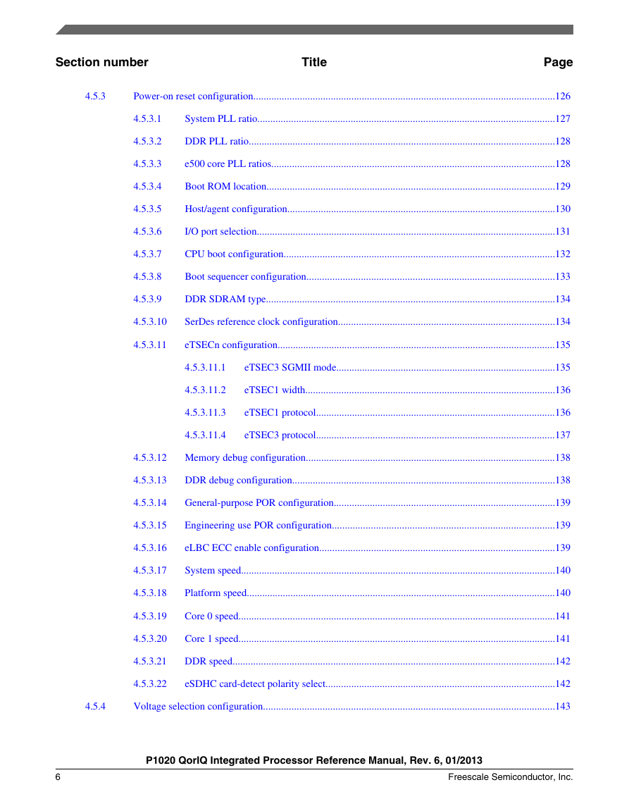
Power-on reset configuration
System PLL ratio
DDR PLL ratio
e500 core PLL ratios
Boot ROM location
Host/agent configuration
I/O port selection
CPU boot configuration
Boot sequencer configuration
DDR SDRAM type
SerDes reference clock configuration
eTSECn configuration
eTSEC3 SGMII mode
eTSEC1 width
eTSEC1 protocol
eTSEC3 protocol
Memory debug configuration
DDR debug configuration
General-purpose POR configuration
Engineering use POR configuration
eLBC ECC enable configuration
System speed
Platform speed
Core 0 speed
Core 1 speed
DDR speed
eSDHC card-detect polarity select
Voltage selection configuration
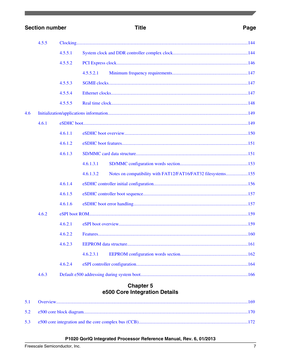
Clocking
System clock and DDR controller complex clock
PCI Express clock
Minimum frequency requirements
SGMII clocks
Ethernet clocks
Real time clock
Initialization/applications information
eSDHC boot
eSDHC boot overview
eSDHC boot features
SD/MMC card data structure
SD/MMC configuration words section
Notes on compatibility with FAT12/FAT16/FAT32 filesystems
eSDHC controller initial configuration
eSDHC controller boot sequence
eSDHC boot error handling
eSPI boot ROM
eSPI boot overview
Features
EEPROM data structure
EEPROM configuration words section
eSPI controller configuration
Default e500 addressing during system boot
Chapter 5: e500 Core Integration Details
Overview
e500 core block diagram
e500 core integration and the core complex bus (CCB)
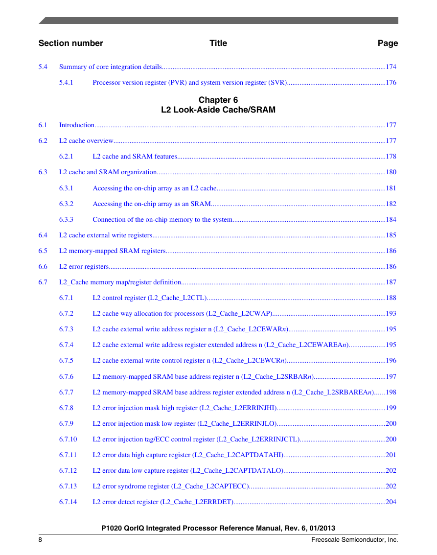
Summary of core integration details
Processor version register (PVR) and system version register (SVR)
Chapter 6: L2 Look-Aside Cache/SRAM
Introduction
L2 cache overview
L2 cache and SRAM features
L2 cache and SRAM organization
Accessing the on-chip array as an L2 cache
Accessing the on-chip array as an SRAM
Connection of the on-chip memory to the system
L2 cache external write registers
L2 memory-mapped SRAM registers
L2 error registers
L2_Cache memory map/register definition
L2_Cache
L2_Cache_L2CTL
L2_Cache_L2CWAP
L2_Cache_L2CEWARn
L2_Cache_L2CEWAREAn
L2_Cache_L2CEWCRn
L2_Cache_L2SRBARn
L2_Cache_L2SRBAREAn
L2_Cache_L2ERRINJHI
L2_Cache_L2ERRINJLO
L2_Cache_L2ERRINJCTL
L2_Cache_L2CAPTDATAHI
L2_Cache_L2CAPTDATALO
L2_Cache_L2CAPTECC
L2_Cache_L2ERRDET
L2_Cache_L2ERRDIS
L2_Cache_L2ERRINTEN
L2_Cache_L2ERRATTR
L2_Cache_L2ERRADDRL
L2_Cache_L2ERRADDRH
L2_Cache_L2ERRCTL
External writes to the L2 cache (cache stashing)
Stash-only cache regions
L2 cache timing
L2 cache and SRAM coherency
L2 cache coherency rules
Memory-mapped SRAM coherency rules
L2 cache locking
Locking the entire L2 cache
Locking programmed memory ranges
Locking selected lines
Clearing locks on selected lines
Flash clearing of instruction and data locks
Locks with stale data
PLRU L2 replacement policy
PLRU bit update considerations
Allocation of lines
L2 cache operation
Initialization
L2 cache initialization
Memory-mapped SRAM initialization
Flash invalidation of the L2 cache
Managing errors
ECC errors
Tag parity errors
L2 cache states
L2 state transitions
Error checking and correcting (ECC)
Chapter 7: e500 Coherency Module
Introduction
Overview
Features
ECM memory map/register definition
ECM
ECM_EEBACR
ECM_EEBPCR
ECM_EIPBRR1
ECM_EIPBRR2
ECM_EEDR
ECM_EEER
ECM_EEATR
ECM_EELADR
ECM_EEHADR
Functional description
I/O arbiter
CCB arbiter
Transaction queue
Global data multiplexor
CCB interface
Initialization/application information
Chapter 8: DDR Memory Controllers
Introduction
Features
Modes of operation
External signal descriptions
Signals overview
Detailed signal descriptions
Memory interface signals
Clock interface signals
DDR memory map/register definition
DDR
DDR_CSn_BNDS
DDR_CSn_CONFIG
DDR_CSn_CONFIG_2
DDR_TIMING_CFG_3
DDR_TIMING_CFG_0
DDR_TIMING_CFG_1
DDR_TIMING_CFG_2
DDR_DDR_SDRAM_CFG
DDR_DDR_SDRAM_CFG_2
DDR_DDR_SDRAM_MODE
DDR_DDR_SDRAM_MODE_2
DDR_DDR_SDRAM_MD_CNTL
DDR_DDR_SDRAM_INTERVAL
DDR_DDR_DATA_INIT
DDR_DDR_SDRAM_CLK_CNTL
DDR_DDR_INIT_ADDR
DDR_DDR_INIT_EXT_ADDR
DDR_TIMING_CFG_4
DDR_TIMING_CFG_5
DDR_DDR_ZQ_CNTL
DDR_DDR_WRLVL_CNTL
DDR_DDR_SR_CNTR
DDR_DDR_SDRAM_RCW_1
DDR_DDR_SDRAM_RCW_2
DDR_DDR_WRLVL_CNTL_2
DDR_DDR_WRLVL_CNTL_3
DDR_DDRDSR_1
DDR_DDRDSR_2
DDR_DDRCDR_1
DDR_DDRCDR_2
DDR_DDR_IP_REV1
DDR_DDR_IP_REV2
DDR_DATA_ERR_INJECT_HI
DDR_DATA_ERR_INJECT_LO
DDR_ERR_INJECT
DDR_CAPTURE_DATA_HI
DDR_CAPTURE_DATA_LO
DDR_CAPTURE_ECC
DDR_ERR_DETECT
DDR_ERR_DISABLE
DDR_ERR_INT_EN
DDR_CAPTURE_ATTRIBUTES
DDR_CAPTURE_ADDRESS
DDR_CAPTURE_EXT_ADDRESS
DDR_ERR_SBE
Functional description
DDR SDRAM interface operation
Supported DDR SDRAM organizations
DDR SDRAM address multiplexing
JEDEC standard DDR SDRAM interface commands
DDR SDRAM interface timing
DDR SDRAM registered DIMM mode
DDR SDRAM write timing adjustments
DDR SDRAM refresh
DDR SDRAM refresh timing
DDR SDRAM refresh and power-saving modes
Self-refresh in sleep mode
DDR data beat ordering
Page mode and logical bank retention
Error checking and correcting (ECC)
Error management
Initialization/application information
Programming differences between memory types
DDR SDRAM initialization sequence
Using Forced Self-Refresh Mode to Implement a Battery-Backed RAM System
Hardware Based Self-Refresh Scheme
Software Based Self-Refresh Scheme
Bypassing Re-initialization During Battery-Backed Operation
Chapter 9: Programmable Interrupt Controller (PIC)
Introduction
Overview
The PIC in multiple-processor implementations
Interrupts to the e500 processor core
Modes of operation
Mixed mode (GCR[M] = 1)
Pass-through mode (GCR[M] = 0)
Interrupt sources
Interrupt routing-mixed mode
Interrupt destinations
Internal interrupt sources
PIC external signal descriptions
Signal overview
Detailed signal descriptions
PIC memory map/register definition
PIC
PIC_BRR1
PIC_BRR2
PIC_IPIDRn
PIC_CTPR
PIC_WHOAMI
PIC_IACK
PIC_EOI
PIC_FRR
PIC_GCR
PIC_VIR
PIC_PIR
PIC_IPIVPRn
PIC_SVR
PIC_TFRRn
PIC_GTCCRAn
PIC_GTBCRAn
PIC_GTVPRAn
PIC_GTDRAn
PIC_TCRn
PIC_ERQSR
PIC_IRQSR0
PIC_IRQSR1
PIC_IRQSR2
PIC_CISR0
PIC_CISR1
PIC_CISR2
PIC_PMnMR0
PIC_PMnMR1
PIC_PMnMR2
PIC_MSGRn
PIC_MER
PIC_MSR
PIC_MSIRn
PIC_MSISR
PIC_MSIIR
PIC_GTCCRBn
PIC_GTBCRBn
PIC_GTVPRBn
PIC_GTDRBn
PIC_MSGRan
PIC_MERa
PIC_MSRa
PIC_EIVPRn
PIC_EIDRn
PIC_IIVPRn
PIC_IIDRn
PIC_MIVPRn
PIC_MIDRn
PIC_MSIVPRn
PIC_MSIDRn
PIC_IPIDR_CPU0n
PIC_CTPR_CPU0
PIC_WHOAMI_CPU0
PIC_IACK_CPU0
PIC_EOI_CPU0
PIC_IPIDR_CPU1n
PIC_CTPR_CPU1
PIC_WHOAMI_CPU1
PIC_IACK_CPU1
PIC_EOI_CPU1
Functional description
Programming model considerations
Global registers
Global timer registers
IRQ_OUT_B and critical interrupt summary registers
Performance monitor mask registers (PMMRs)
Message registers
Shared message signaled registers
Interrupt source configuration registers
Per-CPU (private access) registers
Flow of interrupt control
Interrupts routed to cint or IRQ_OUT_B
Interrupts routed to int
Interrupt source priority
Interrupt acknowledge
Spurious vector generation
Nesting of interrupts
Interprocessor interrupts
Message interrupts
Shared message signaled interrupts
PCI Express INTx/IRQn sharing
Global timers
Resets
Resetting the PIC
Processor core initialization
Initialization/application information
Programming guidelines
PIC registers
Changing interrupt source configuration
Chapter 10: I2C Interfaces
Overview
Introduction to I2C
What is the I2C module?
I2C module block diagram
Features
Advantages of the I2C bus
Modes of operation
I2C-specific conditions
I2C external signal descriptions
Signal overview
Detailed signal descriptions
I2C memory map/register definition
I2Cx
I2Cx_I2CADR
I2Cx_I2CFDR
I2Cx_I2CCR
I2Cx_I2CSR
I2Cx_I2CDR
I2Cx_I2CDFSRR
Functional description
Transaction protocol
START condition
Slave address transmission
Repeated START condition
STOP condition
Protocol implementation details
Transaction monitoring-implementation details
Control transfer-implementation details
Address compare-implementation details
Arbitration procedure
Arbitration control
Handshaking
Clock control
Clock synchronization
Input synchronization and digital filter
Input signal synchronization
Filtering of SCL and SDA lines
Clock stretching
Boot sequencer mode
EEPROM calling address
EEPROM data format
Initialization/application information
Initialization sequence
Generation of START
Post-transfer software response
Generation of STOP
Generation of repeated START
Generation of SCL when SDA low
Slave mode interrupt service routine
Slave transmitter and received acknowledge
Loss of arbitration and forcing of slave mode
Interrupt service routine flowchart
Chapter 11: DUART
Introduction
Overview
Features
Modes of operation
DUART external signal descriptions
DUART memory map/register definition
DUART
DUART_URBRn
DUART_UTHRn
DUART_UDLBn
DUART_UDMBn
DUART_UIERn
DUART_UIIRn
DUART_UFCRn
DUART_UAFRn
DUART_ULCRn
DUART_UMCRn
DUART_ULSRn
DUART_UMSRn
DUART_USCRn
DUART_UDSRn
Functional description
Serial interface
START bit
Data transfer
Parity bit
STOP bit
Baud-rate generator logic
Local loopback mode
Errors
Framing error
Parity error
Overrun error
FIFO mode
FIFO interrupts
DMA mode select
Interrupt control logic
DUART initialization/application information
Chapter 12: Enhanced local bus controller (eLBC)
eLBC introduction
Overview
Features
Modes of operation
eLBC bus clock and clock ratios
Source ID debug mode
eLBC external signal descriptions
Enhanced Local Bus Controller (eLBC) Memory Map
eLBC
eLBC_BR0
eLBC_ORg0
eLBC_ORf0
eLBC_ORu0
eLBC_BRn
eLBC_ORgn
eLBC_ORfn
eLBC_ORun
eLBC_MAR
eLBC_MnMR
eLBC_MRTPR
eLBC_MDRu
eLBC_MDRf
eLBC_LSOR
eLBC_LURT
eLBC_LTESR
eLBC_LTEDR
eLBC_LTEIR
eLBC_LTEATR
eLBC_LTEAR
eLBC_LTECCR
eLBC_LBCR
eLBC_LCRR
eLBC_FMR
eLBC_FIR
eLBC_FCR
eLBC_FBAR
eLBC_FPARl
eLBC_FPARs
eLBC_FBCR
eLBC_FECCn
eLBC functional description
Basic architecture
Address and address space checking
External address latch enable signal (LALE)
Data transfer acknowledge (TA)
Data buffer control (LBCTL)
Parity generation and checking (LDP)
Bus monitor
PLL Bypass mode
General-purpose chip-select machine (GPCM)
GPCM read signal timing
GPCM write signal timing
Chip-select assertion timing
Programmable wait state configuration
Chip-select and write enable negation timing
Relaxed timing
Output enable (LOE_B) timing
Extended hold time on read accesses-GPCM
External access termination (LGTA_B)
GPCM boot chip-select operation
Flash control machine (FCM)
FCM buffer RAM
Buffer layout and page mapping for small-page NAND flash devices
Buffer layout and page mapping for large-page NAND flash devices
Error correcting codes and the spare region
Programming FCM
FCM command instructions
FCM no-operation instruction
FCM address instructions
FCM data read instructions
FCM data write instructions
FCM signal timing
FCM chip-select timing
FCM command, address, and write data timing
FCM ready/busy timing
FCM read data timing
FCM extended read hold timing
FCM boot chip-select operation
FCM bank 0 reset initialization
Boot block loading into the FCM buffer RAM
User-programmable machines (UPMs)
UPM requests
Memory access requests
UPM refresh timer requests
Software requests-RUN command
Exception requests
Programming the UPMs
UPM programming example (two sequential writes to the RAM array)
UPM programming example (two sequential reads from the RAM array)
UPM signal timing
RAM array
RAM words
Chip-select signal timing (CSTn)
Byte select signal timing (BSTn)
General-purpose signals (GnTn, GOn)
Loop control (LOOP)
Repeat execution of current RAM word (REDO)
Address multiplexing (AMX)
Data valid and data sample control (UTA)
LGPL[0:5] signal negation (LAST)
Wait mechanism (WAEN)
Extended hold time on read accesses-UPM
eLBC initialization/application information
Interfacing to peripherals in different address modes
Non-multiplexed address and data buses
Multiplexed address and data to save maximum pins in 8- to 16-bit addressing
Peripheral hierarchy on the local bus for high bus speeds
GPCM timings
Bus turnaround
Address phase after previous read
Read data phase after address phase
Read-modify-write cycle for parity protected memory banks
UPM cycles with additional address phases
Interface to different port-size devices
Command sequence examples for NAND flash EEPROM
NAND flash soft reset command sequence example
NAND flash read status command sequence example
NAND flash read identification command sequence example
NAND flash page read command sequence example
NAND flash block erase command sequence example
NAND flash program command sequence example
Interfacing to fast-page mode DRAM using UPM
Interfacing to ZBT SRAM using UPM
Chapter 13: DMA Controller
DMA overview
DMA features summary
DMA modes of operation
DMA external signal description
Signal overview
DMA signal descriptions
DMA controller memory map
DMA
DMA_MRn
DMA_SRn
DMA_ECLNDARn
DMA_CLNDARn
DMA_SATRn
DMA_SARn
DMA_DATRn
DMA_DARn
DMA_BCRn
DMA_ENLNDARn
DMA_NLNDARn
DMA_ECLSDARn
DMA_CLSDARn
DMA_ENLSDARn
DMA_NLSDARn
DMA_SSRn
DMA_DSRn
DMA_DGSR
DMA functional description
DMA channel operation
Source/destination transaction size calculations
Basic DMA mode transfer
Basic direct mode
Basic, direct, single-write start mode
Basic chaining mode
Basic chaining, single-write start mode
Extended DMA mode transfer
Extended direct mode
Extended direct, single-write start mode
Extended chaining mode
Extended chaining, single-write start mode
External control mode transfer
Channel continue mode for cascading transfer chains
Basic mode
Extended mode
Channel abort
Bandwidth control
Channel state
Illustration of stride size and stride distance
DMA transfer interfaces
DMA errors
DMA descriptors
DMA controller limitations and restrictions
DMA system considerations
Unusual DMA scenarios
DMA to core
DMA to configuration, control, and status registers (CCSR)
DMA to I2C
DMA to DUART
Chapter 14: PCI Express Interface Controller
Introduction
Outbound transactions
Inbound transactions
PCI Express features summary
PCI Express modes of operation
Root complex/endpoint modes
Link width
PCI Express signal descriptions
Memory map/register overview
PCI Express memory-mapped registers
PEXx
PEXx_PEX_CONFIG_ADDR
PEXx_PEX_CONFIG_DATA
PEXx_PEX_OTB_CPL_TOR
PEXx_PEX_CONF_RTY_TOR
PEXx_PEX_CONFIG
PEXx_PEX_PME_MES_DR
PEXx_PEX_PME_MES_DISR
PEXx_PEX_PME_MES_IER
PEXx_PEX_PMCR
PEXx_PEX_IP_BLK_REV1
PEXx_PEX_IP_BLK_REV2
PEXx_PEXOTARn
PEXx_PEXOTEARn
PEXx_PEXOWAR0
PEXx_PEXOWBARn
PEXx_PEXOWARn
PEXx_PEXOWAR3
PEXx_PEXOWAR4
PEXx_PEXITARn
PEXx_PEXIWBARn
PEXx_PEXIWBEARn
PEXx_PEXIWARn
PEXx_PEX_ERR_DR
PEXx_PEX_ERR_EN
PEXx_PEX_ERR_DISR
PEXx_PEX_ERR_CAP_STAT
PEXx_PEX_ERR_CAP_Rn
PCI Express configuration-space registers
PCI compatible configuration headers
Type 0 configuration header registers
Vendor_ID_Register
Device_ID_Register
Command_Register
Status_Register
Revision_ID_Register
Class_Code_Register
Cache_Line_Size_Register
Latency_Timer_Register
Header_Type_Register
PEXCSRBAR
BAR1
BARn
BARn
Subsystem_Vendor_ID_Register
Subsystem_ID_Register
Capabilities_Pointer_Register
Interrupt_Line_Register
Interrupt_Pin_Register
Minimum_Grant_Register
Maximum_Latency_Register
Type 1 configuration header registers
PEXCSRBAR
Primary_Bus_Number_Register
Secondary_Bus_Number_Register
Subordinate_Bus_Number_Register
IO_Base_Register
IO_Limit_Register
Secondary_Status_Register
Memory_Base_Register
Memory_Limit_Register
Prefetchable_Memory_Base_Register
Prefetchable_Memory_Limit_Register
Prefetchable_Base_Upper_32_Bits_Register
Prefetchable_Limit_Upper_32_Bits_Register
IO_Base_Upper_16_Bits_Register
IO_Limit_Upper_16_Bits_Register
Capabilities_Pointer_Register
Interrupt_Line_Register
Interrupt_Pin_Register
Bridge_Control_Register
PCI compatible device-specific configuration space
Power_Management_Capability_ID_Register
Power_Management_Capabilities_Register
Power_Management_Status_and_Control_Register
Power_Management_Data_Register
Capability_ID_Register
Capabilities_Register
Device_Capabilities_Register
Device_Control_Register
Device_Status_Register
Link_Capabilities_Register
Link_Control_Register
Link_Status_Register
Slot_Capabilities_Register
Slot_Control_Register
Slot_Status_Register
Root_Control_Register
Root_Status_Register
MSI_Message_Capability_ID_Register
MSI_Message_Control_Register
MSI_Message_Address_Register
MSI_Message_Upper_Address_Register
MSI_Message_Data_Register
PCI Express extended configuration space
Advanced_Error_Reporting_Capability_ID_Register
Uncorrectable_Error_Status_Register
Uncorrectable_Error_Mask_Register
Uncorrectable_Error_Severity_Register
Correctable_Error_Status_Register
Correctable_Error_Mask_Register
Advanced_Error_Capabilities_and_Control_Register
Header_Log_Register_DWORD1
Header_Log_Register_DWORD2
Header_Log_Register_DWORD3
Header_Log_Register_DWORD4
Root_Error_Command_Register
Root_Error_Status_Register
Correctable_Error_Source_ID_Register
Error_Source_ID_Register
LTSSM_State_Status_Register
Controller_Core_Clock_Ratio_Register
Power_Management_Timer_Register
PME_Time_Out_Register
Subsystem_Vendor_ID_Update_Register
Configuration_Ready_Register
Flow_Control_Update_Timeout_Register
Secondary_Status_Interrupt_Mask_Register
Functional description
Architecture
PCI Express transactions
Byte ordering
Address invariance
Byte order for configuration transactions
Lane reversal
Transaction ordering rules
PCI Express outbound ATMUs
PCI Express inbound ATMUs
EP inbound ATMU implementation
RC inbound ATMU implementation
Memory space addressing
I/O space addressing
Configuration space addressing
PCI Express configuration space access
RC configuration register access
EP configuration register access
Serialization of configuration and I/O writes
Messages
Outbound ATMU message generation
Inbound messages
Error handling
PCI Express error logging and signaling
PCI Express controller internal interrupt sources
Error conditions
Error capture registers
Error capture registers (outbound error)
Error capture registers (inbound error)
Interrupts
EP interrupt generation
Hardware INTx message generation
Hardware MSI generation
Software INTx message generation
Software MSI generation
RC handling of INTx message and MSI interrupts
INTx message handling
MSI handling
Initial credit advertisement
Power management
L2/L3 ready link state
Hot reset
Link down
Initialization/application information
EP Boot mode and inbound configuration transactions
Automatic link retraining during initialization
Configuration accesses and inbound writes to CCSR space
Chapter 15: Enhanced Three-Speed Ethernet Controllers
Overview
Features
Modes of operation
eTSEC external signals description
Detailed signal descriptions
eTSEC memory map/register definition
Top-level module memory map
eTSECx
eTSECx_TSEC_ID
eTSECx_TSEC_ID2
eTSECx_IEVENTGn
eTSECx_IMASKGn
eTSECx_EDIS
eTSECx_EMAPG
eTSECx_ECNTRL
eTSECx_PTV
eTSECx_DMACTRL
eTSECx_TBIPA
eTSECx_TCTRL
eTSECx_TSTATn
eTSECx_DFVLAN
eTSECx_TXIC
eTSECx_TQUEUE
eTSECx_TR03WT
eTSECx_TR47WT
eTSECx_TBDBPH
eTSECx_TBPTRn
eTSECx_TBASEH
eTSECx_TBASEn
eTSECx_TMR_TXTSn_ID
eTSECx_TMR_TXTSn_H
eTSECx_TMR_TXTSn_L
eTSECx_RCTRL
eTSECx_RSTATn
eTSECx_RXIC
eTSECx_RQUEUE
eTSECx_RIRn
eTSECx_RBIFX
eTSECx_RQFAR
eTSECx_RQFCR
eTSECx_RQFPR
eTSECx_MRBLR
eTSECx_RPWT
eTSECx_RBDBPH
eTSECx_RBPTRn
eTSECx_RBASEH
eTSECx_RBASEn
eTSECx_TMR_RXTS_H
eTSECx_TMR_RXTS_L
eTSECx_MACCFG1
eTSECx_MACCFG2
eTSECx_IPGIFG
eTSECx_HAFDUP
eTSECx_MAXFRM
eTSECx_IFSTAT
eTSECx_MACSTNADDR1
eTSECx_MACSTNADDR2
eTSECx_MACnADDR1
eTSECx_MACnADDR2
eTSECx_TR64
eTSECx_TR127
eTSECx_TR255
eTSECx_TR511
eTSECx_TR1K
eTSECx_TRMAX
eTSECx_TRMGV
eTSECx_RBYT
eTSECx_RPKT
eTSECx_RFCS
eTSECx_RMCA
eTSECx_RBCA
eTSECx_RXCF
eTSECx_RXPF
eTSECx_RXUO
eTSECx_RALN
eTSECx_RFLR
eTSECx_RCDE
eTSECx_RCSE
eTSECx_RUND
eTSECx_ROVR
eTSECx_RFRG
eTSECx_RJBR
eTSECx_RDRP
eTSECx_TBYT
eTSECx_TPKT
eTSECx_TMCA
eTSECx_TBCA
eTSECx_TXPF
eTSECx_TDFR
eTSECx_TEDF
eTSECx_TSCL
eTSECx_TMCL
eTSECx_TLCL
eTSECx_TXCL
eTSECx_TNCL
eTSECx_TDRP
eTSECx_TJBR
eTSECx_TFCS
eTSECx_TXCF
eTSECx_TOVR
eTSECx_TUND
eTSECx_TFRG
eTSECx_CAR1
eTSECx_CAR2
eTSECx_CAM1
eTSECx_CAM2
eTSECx_RREJ
eTSECx_IGADDRn
eTSECx_GADDRn
eTSECx_ATTR
eTSECx_ATTRELI
eTSECx_RQPRMn
eTSECx_RFBPTRn
eTSECx_ISRGn
eTSECx_RXICn
eTSECx_TXICn
eTSEC IEEE 1588 PTP memory map/register definition
eTSEC1x
eTSEC1x_TMR_CTRL
eTSEC1x_TMR_TEVENT
eTSEC1x_TMR_TEMASK
eTSEC1x_TMR_PEVENT
eTSEC1x_TMR_PEMASK
eTSEC1x_TMR_STAT
eTSEC1x_TMR_CNT_H
eTSEC1x_TMR_CNT_L
eTSEC1x_TMR_ADD
eTSEC1x_TMR_ACC
eTSEC1x_TMR_PRSC
eTSEC1x_TMROFF_H
eTSEC1x_TMROFF_L
eTSEC1x_TMR_ALARMn_H
eTSEC1x_TMR_ALARMn_L
eTSEC1x_TMR_FIPERn
eTSEC1x_TMR_ETTSn_H
eTSEC1x_TMR_ETTSn_L
MDIO memory map/register definition
eTSECx_MDIO
eTSECx_MDIO_IEVENTM
eTSECx_MDIO_IMASKM
eTSECx_MDIO_EMAPM
eTSECx_MDIO_MIIMCFG
eTSECx_MDIO_MIIMCOM
eTSECx_MDIO_MIIMADD
eTSECx_MDIO_MIIMCON
eTSECx_MDIO_MIIMSTAT
eTSECx_MDIO_MIIMIND
TBI memory map/register definition
TBI_MII_Register_Set
TBI_MII_Register_Set_CR
TBI_MII_Register_Set_SR
TBI_MII_Register_Set_ANA
TBI_MII_Register_Set_ANA_SGMII
TBI_MII_Register_Set_ANLPBPA
TBI_MII_Register_Set_ANLPBPA_SGMII
TBI_MII_Register_Set_ANEX
TBI_MII_Register_Set_ANNPT
TBI_MII_Register_Set_ANLPANP
TBI_MII_Register_Set_EXST
TBI_MII_Register_Set_JD
TBI_MII_Register_Set_TBICON
Functional description
Programming model considerations
MAC functionality
Configuring the MAC
Controlling CSMA/CD
Handling packet collisions
Controlling packet flow
Controlling PHY links
MIB registers
Hash function registers
Lossless flow control configuration registers
Hardware assist for IEEE1588 compliant timestamping
Interrupt steering and coalescing registers
Ten-bit interface (TBI)
Connecting to physical interfaces on Ethernet
Media-independent interface (MII)
Reduced media-independent interface (RMII)
Reduced gigabit media-independent interface (RGMII)
Serial gigabit media-independent interface (SGMII)
SGMII interface
Gigabit Ethernet controller channel operation
Initialization sequence
Hardware controlled initialization
User initialization
Soft reset and reconfiguring procedure
Timer soft reset and reconfiguring procedure
Gigabit Ethernet frame transmission
Gigabit Ethernet frame reception
Ethernet preamble customization
User-defined preamble transmission
User-visible preamble reception
RMON support
Frame recognition
Destination address recognition and frame filtering
Hash table algorithm
Magic Packet mode
Flow control
Grouping of rings
Interrupt handling
Interrupt coalescing
Interrupt coalescing by frame count threshold
Interrupt coalescing by timer threshold
Interframe gap time
Internal and external loop back
Error-handling procedure
TCP/IP offload
Frame control blocks
Transmit path off-load and Tx PTP packet parsing
Receive path offload
Quality of service (QoS) provision
Receive parser
Receive queue filer
Filing rules
Comparing properties with bit masks
Special-case rules
Filer hash engine
Ring index mapping logic
Hash function
Filer interrupt events
Setting up the receive queue filer table
Filer example-802.1p priority filing
Filer example-IP diff-serv code points filing
Filer example-TCP and UDP port filing
Filer example-hash on AND chain (2-tuple)
Filer example-hash on AND chain (3-tuple)
Filer example-hash on AND chain (5-tuple)
Filer example-hash on cluster rules
Filer example-hash on compound rule
Filer example-interrupt from deep sleep
Transmission scheduling
Priority-based queuing (PBQ)
Modified weighted round-robin queuing (MWRR)
Lossless flow control
Back pressure determination through free buffers
Software use of hardware-initiated back pressure
Initialization
Operation
Hardware assist for IEEE Std. 1588 compliant timestamping
Features
Timer logic overview
Time stamp insertion on the received packets
Time stamp point
PTP packet parsing
General purpose filer rule
Time stamp insertion on transmit packets
Interrupts
Error condition
Tx PTP packet parsing
Buffer descriptors
Data buffer descriptors
Transmit data buffer descriptors (TxBD)
Receive buffer descriptors (RxBD)
Initialization/application information
Interface mode configuration
MII interface mode
RMII interface mode
RGMII interface mode
SGMII interface support
Multigroup mode initialization
Chapter 16: Enhanced secure digital host controller (eSDHC)
eSDHC overview
eSDHC features summary
Data transfer modes
eSDHC external signal description
Enhanced Secure Digital Host Controller (eSDHC) Memory Map
eSDHC
eSDHC_DSADDR
eSDHC_BLKATTR
eSDHC_CMDARG
eSDHC_XFERTYP
eSDHC_CMDRSPn
eSDHC_DATPORT
eSDHC_PRSSTAT
eSDHC_PROCTL
eSDHC_SYSCTL
eSDHC_IRQSTAT
eSDHC_IRQSTATEN
eSDHC_IRQSIGEN
eSDHC_AUTOC12ERR
eSDHC_HOSTCAPBLT
eSDHC_WML
eSDHC_FEVT
eSDHC_HOSTVER
eSDHC_DCR
eSDHC functional description
Data buffer
Write operation sequence
Read operation sequence
Data buffer size
DMA CCB interface
Internal DMA request
DMA burst length
CCB Master interface
SD protocol unit
SD transceiver
SD clock and monitor
Command agent
Data agent
Clock and reset manager
Clock generator
Card insertion and removal detection
Power management and wake-up events
Setting wake-up events
Initialization/application information
Command send and response receive basic operation
Card identification mode
Card detect
Reset
Voltage validation
Card registry
Card access
Block write
Normal write
Write with pause
Block read
Normal read
Read with pause
Transfer error
CRC error
Internal DMA error
Auto CMD12 error
Card interrupt
Switch function
Query, enable and disable SD high speed mode
Query, enable and disable MMC high speed mode
Set MMC bus width
Commands for MMC/SD
Software restrictions
Chapter 17: Universal Serial Bus Interface
Introduction
Overview
Features
Modes of operation
USB external signals
ULPI interface
PHY clocks
USB memory map/register definition
USBx
USBx_ID
USBx_CAPLENGTH
USBx_HCIVERSION
USBx_HCSPARAMS
USBx_HCCPARAMS
USBx_DCIVERSION
USBx_DCCPARAMS
USBx_USBCMD
USBx_USBSTS
USBx_USBINTR
USBx_FRINDEX
USBx_PERIODICLISTBASE
USBx_DEVICEADDR
USBx_ASYNCLISTADDR
USBx_ENDPOINTLISTADDR
USBx_BURSTSIZE
USBx_TXFILLTUNING
USBx_ULPI_VIEWPORT
USBx_CONFIGFLAG
USBx_PORTSC
USBx_USBMODE
USBx_ENDPTSETUPSTAT
USBx_ENDPOINTPRIME
USBx_ENDPTFLUSH
USBx_ENDPTSTATUS
USBx_ENDPTCOMPLETE
USBx_ENDPTCTRL0
USBx_ENDPTCTRLn
USBx_SNOOPn
USBx_AGE_CNT_THRESH
USBx_PRI_CTRL
USBx_SI_CTRL
USBx_CONTROL
Functional description
System interface
DMA engine
FIFO RAM controller
PHY interface
Host data structures
Periodic frame list
Asynchronous list queue head pointer
Isochronous (high-speed) transfer descriptor (iTD)
Next link pointer-iTD
iTD transaction status and control list
iTD buffer page pointer list (plus)
Split transaction isochronous transfer descriptor (siTD)
Next link pointer-siTD
siTD endpoint capabilities/characteristics
siTD transfer state
siTD buffer pointer list (plus)
siTD back link pointer
Queue element transfer descriptor (qTD)
Next qTD pointer
Alternate next qTD pointer
qTD token
qTD buffer page pointer list
Queue head
Queue head horizontal link pointer
Endpoint capabilities/characteristics
Transfer overlay
Periodic frame span traversal node (FSTN)
FSTN normal path pointer
FSTN back path link pointer
Host operations
Host controller initialization
Power port
Reporting over-current
Suspend/resume
Port suspend/resume
Schedule traversal rules
Periodic schedule frame boundaries vs. bus frame boundaries
Periodic schedule
Managing isochronous transfers using iTDs
Host controller operational model for iTDs
Software operational model for iTDs
Periodic scheduling threshold
Asynchronous schedule
Adding queue heads to asynchronous schedule
Removing queue heads from asynchronous schedule
Empty asynchronous schedule detection
Asynchronous schedule traversal: Start event
Reclamation status bit (USBSTS Register)
Managing control/bulk/interrupt transfers via queue heads
Buffer pointer list use for data streaming with qTDs
Adding interrupt queue heads to the periodic schedule
Managing transfer complete interrupts from queue heads
Ping control
Split transactions
Split transactions for asynchronous transfers
Asynchronous-do-start-split
Asynchronous-do-complete-split
Split transaction interrupt
Split transaction scheduling mechanisms for interrupt
Host controller operational model for FSTNs
Software operational model for FSTNs
Tracking split transaction progress for interrupt transfers
Split transaction execution state machine for interrupt
Periodic interrupt-do-start-split
Periodic interrupt-do-complete-split
Managing the QH[FrameTag] field
Rebalancing the periodic schedule
Split transaction isochronous
Split transaction scheduling mechanisms for isochronous
Tracking split transaction progress for isochronous transfers
Split transaction execution state machine for isochronous
Periodic isochronous-do-start-split
Periodic isochronous-do complete split
Complete-split for scheduling boundary cases 2a, 2b
Split transaction for isochronous-processing example
Port test modes
Interrupts
Transfer/transaction based interrupts
Transaction error
Serial bus babble
Data buffer error
USB interrupt (interrupt on completion (IOC))
Short packet
Host controller event interrupts
Port change events
Frame list rollover
Interrupt on async advance
Host system error
Device data structures
Endpoint queue head
Endpoint capabilities/characteristics
Transfer overlay
Current dTD pointer
Setup buffer
Endpoint transfer descriptor (dTD)
Device operational model
Device controller initialization
Port state and control
Bus reset
Suspend/resume
Suspend description
Suspend operational model
Resume
Managing endpoints
Endpoint initialization
Stalling
Data toggle
Data toggle reset
Data toggle inhibit
Device operational model for packet transfers
Priming transmit endpoints
Priming receive endpoints
Interrupt/bulk endpoint operational model
Interrupt/bulk endpoint bus response matrix
Control endpoint operation model
Setup phase
Data phase
Status phase
Control endpoint bus response matrix
Isochronous endpoint operational model
Isochronous pipe synchronization
Isochronous endpoint bus response matrix
Managing queue heads
Queue head initialization
Operational model for setup transfers
Managing transfers with transfer descriptors
Software link pointers
Building a transfer descriptor
Executing a transfer descriptor
Transfer completion
Flushing/depriming an endpoint
Device error matrix
Servicing interrupts
High-frequency interrupts
Low-frequency interrupts
Error interrupts
Deviations from the EHCI specifications
Embedded transaction translator function
Capability registers
Operational registers
Discovery
Data structures
Operational model
Microframe pipeline
Split state machines
Asynchronous transaction scheduling and buffer management
Periodic transaction scheduling and buffer management
Multiple transaction translators
Device operation
Non-zero fields the register file
SOF interrupt
Embedded design
Frame adjust register
Miscellaneous variations from EHCI
Discovery
Port reset
Port speed detection
Chapter 18: Enhanced Serial Peripheral Interface
Introduction
Features
eSPI transmission and reception process
Modes of operation
External signal descriptions
Overview
ESPI detailed signal descriptions
Enhanced serial peripheral interface (eSPI) memory map
ESPI
ESPI_SPMODE
ESPI_SPIE
ESPI_SPIM
ESPI_SPCOM
ESPI_SPITF
ESPI_SPIRF
ESPI_SPMODE0
ESPI_SPMODE1
ESPI_SPMODE2
ESPI_SPMODE3
eSPI transfer formats
CI and CP values for various eSPI devices
eSPI programming examples
24-bit address example
16-bit address example
Chapter 19: Time Division Multiplexing (TDM)
Introduction
TDM features
TDM signal descriptions
TDM signals overview
TDM external signals descriptions
TDM overview
TDM basics
Common signals for the TDM modules
TDM programming model
SB interface
TDM_SB memory map/register definition
TDM_SB
TDM_SB_TDMGIR
TDM_SB_TDMRIR
TDM_SB_TDMTIR
TDM_SB_TDMRFP
TDM_SB_TDMTFP
TDM_SB_TDMRCENn
TDM_SB_TDMTCENn
TDM_SB_TDMTCMAn
TDM_SB_TDMRCR
TDM_SB_TDMTCR
TDM_SB_TDMRIER
TDM_SB_TDMTIER
TDM_SB_TDMRER
TDM_SB_TDMTER
TDM_SB_TDMRSR
TDM_SB_TDMTSR
AHB interface
TDM_AHB memory map/register definition
TDM_AHB
TDM_AHB_TDMRDREG
TDM_AHB_TDMTDREG
Clocks and reset
TDM clock and frame sync generation
Reset
TDM configurations
Typical configurations
TDM detailed operation
Serial interface
Sync out configuration
Sync in configuration
Serial interface synchronization
Reverse data order
Receiver and transmitter independent or shared operation
TDM multichannel (network) mode
Operation using Tx channel mask register
Operation using Rx channel enable register
Data structures
FIFO configuration
DMA configuration
Setting up the TDM for correct operation with the DMA
Software programming
Software programming sequence
Initialization-shared operation starting on the same frame
Initialization-non-shared operation
Dynamic channel configuration while TDM operating-shared
Dynamic channel configuration while TDM operating-non-shared
Configuring the TDM for I2S operation
TDM power down
Synchronization errors
Interrupts
Receiver normal and receiver error interrupts
Transmit normal and transmit error TDMRDREG
DMA controller (DMAC)
Overview
DMAC features
TDM_DMAC memory map/register definition
TDM_DMAC
TDM_DMAC_DMACR
TDM_DMAC_DMAES
TDM_DMAC_DMAERQ
TDM_DMAC_ DMAEEI
TDM_DMAC_DMASERQ
TDM_DMAC_DMACERQ
TDM_DMAC_DMASEEI
TDM_DMAC_DMACEEI
TDM_DMAC_DMACINT
TDM_DMAC_DMACERR
TDM_DMAC_DMASSRT
TDM_DMAC_DMACDNE
TDM_DMAC_DMAINT
TDM_DMAC_ DMAERR
TDM_DMAC_ DMAHRS
TDM_DMAC_DMAGPOR
TDM_DMAC_DCHPRIn
TDM_DMAC_TCDW0
TDM_DMAC_TCDW1
TDM_DMAC_TCDW2
TDM_DMAC_TCDW3
TDM_DMAC_TCDW4
TDM_DMAC_TCDW5
TDM_DMAC_TCDW6
TDM_DMAC_TCDW7
Functional description
DMA microarchitecture
DMA basic data flow
Initialization/application information
DMA initialization
DMA programming errors
DMA transfer
Single request
Multiple requests
TCD status
Minor loop complete
Active channel TCD reads
Hardware request release timing
Chapter 20: General-Purpose I/O (GPIO) Module
Introduction
Overview
Features
External signal description
Signals overview
GPIO memory map/register definition
GPIO
GPIO_GPDIR
GPIO_GPODR
GPIO_GPDAT
GPIO_GPIER
GPIO_GPIMR
GPIO_GPICR
Chapter 21: Device Performance Monitor
Introduction
Overview
Features
Signal descriptions
PERFMON Memory Map/Register Definition
PERFMON
PERFMON_PMGC0
PERFMON_PMLCA0
PERFMON_PMLCB0
PERFMON_PMC0_upper
PERFMON_PMC0_lower
PERFMON_PMLCAn
PERFMON_PMLCBn
PERFMON_PMCn
Functional description
Performance monitor interrupt
Event counting
Threshold events
Chaining
Triggering
Burstiness counting
Performance monitor events
Performance monitor examples
Initialization/application information
Chapter 22: Global Utilities
Introduction
Overview
Global utilities features
Power management and block disables
Accessing current POR configuration settings
Clock control
Global utilities external signal description
Signals overview
Detailed signal descriptions
GUTS Memory Map/Register Definition
GUTS
GUTS_PORPLLSR
GUTS_PORBMSR
GUTS_PORDEVSR
GUTS_PORDBGMSR
GUTS_PORDEVSR2
GUTS_GPPORCR
GUTS_PMUXCR
GUTS_DEVDISR
GUTS_POWMGTCSR
GUTS_PMCDR
GUTS_MCPSUMR
GUTS_RSTRSCR
GUTS_ECTRSTCR
GUTS_AUTORSTSR
GUTS_PVR
GUTS_SVR
GUTS_RSTCR
GUTS_IOVSELSR
GUTS_DDRCLKDR
GUTS_CLKOCR
GUTS_ECMCR
GUTS_SRDSCR0
GUTS_SRDSCR1
GUTS_SRDSCR2
GUTS_SRDSCR3
GUTS_SRDSCR4
Functional description
Power management
Relationship between both cores and device power management states
CKSTP_IN0/1_B is not power management
Dynamic power management
Shutting down unused blocks
Software-controlled power-down states
Doze mode
Nap mode
Sleep mode
Power management control fields
Power-down sequence coordination
Interrupts and power management
Interrupts and power management controlled by MSR[WE]
Interrupts and power management controlled by POWMGTCSR
Snooping in power down modes
Software considerations for power management
Requirements for reaching and recovering from sleep state
Chapter 23: Debug Features and Watchpoint Facility
Introduction
Overview
Features
Modes of operation
Memory debug mode (eLBC and DDR)
DDR SDRAM interface debug mode
Watchpoint monitor modes
Trace buffer modes
Debug external signal description
Signals overview
Detailed signal descriptions
Debug signals-details
Watchpoint monitor trigger signals-details
JTAG test signals-details
Debug Memory Map/Register Definition
debug
debug_WMCR0
debug_WMCR1
debug_WMAR
debug_WMAMR
debug_WMTMR
debug_WMSR
debug_TBCR0
debug_TBCR1
debug_TBAR
debug_TBAMR
debug_TBTMR
debug_TBSR
debug_TBACR
debug_TBADHR
debug_TBADR
debug_PCIDR
debug_CCIDR
debug_TOSR
Functional description
Source and target ID
DDR SDRAM interface debug
Debug information on debug pins
Debug information on ECC pins
Local bus interface debug
Watchpoint monitor
Watchpoint monitor performance monitor events
Trace buffer
Traced data formats (as a function of TBCR1[IFSEL])
Initialization
Appendix A: Terminology, Conventions, and Resources
About this content
Acronyms and abbreviations
Notational conventions
Related resources
Appendix B: P1011–A Single Core Version
Overview
Appendix C: Substantive changes from revision 5 to revision 6
Overview Revision History
Memory Map Revision History
Signal Descriptions Revision History
Reset, Clocking, and Initialization Revision History
e500 Core Integration Details Revision History
DDR Memory Controllers Revision History
Programmable Interrupt Controller (PIC) Revision History
Enhanced Local Bus Controller (eLBC) Revision History
DMA Controller Revision History
PCI Express Interface Controller Revision History
Enhanced Three-Speed Ethernet Controllers Revision History
Enhanced Secure Digital Host Controller Revision History
Universal Serial Bus Interface Revision History
Enhanced Serial Peripheral Interface Revision History
Time Division Multiplexing (TDM) Interface Revision History
Device Performance Monitor Revision History
Global Utilities Revision History
Debug Features and Watchpoint Facility Revision History



 2023年江西萍乡中考道德与法治真题及答案.doc
 2012年重庆南川中考生物真题及答案.doc
 2013年江西师范大学地理学综合及文艺理论基础考研真题.doc
 2020年四川甘孜小升初语文真题及答案I卷.doc
 2020年注册岩土工程师专业基础考试真题及答案.doc
 2023-2024学年福建省厦门市九年级上学期数学月考试题及答案.doc
 2021-2022学年辽宁省沈阳市大东区九年级上学期语文期末试题及答案.doc
 2022-2023学年北京东城区初三第一学期物理期末试卷及答案.doc
 2018上半年江西教师资格初中地理学科知识与教学能力真题及答案.doc
 2012年河北国家公务员申论考试真题及答案-省级.doc
 2020-2021学年江苏省扬州市江都区邵樊片九年级上学期数学第一次质量检测试题及答案.doc
 2022下半年黑龙江教师资格证中学综合素质真题及答案.doc