Figures
Tables
Release History
1 Introduction
1.1 Scope
1.2 Purpose
2 Terminology (Informative)
2.1 Use of Special Terms
2.2 Number Radix
2.3 Definitions
2.4 Abbreviations
2.5 Acronyms
3 References
3.1 Display Bus Interface Standard for Parallel Signaling (DBI-2)
3.2 Display Pixel Interface Standard for Parallel Signaling (DPI-2)
3.3 MIPI Alliance Specification for Display Command Set (DCS)
3.4 (Blank Section)
3.5 Physical Layer Definition for DSI
3.5.1 MIPI Alliance Specification for D-PHY (D-PHY)
3.5.2 MIPI Alliance Specification for C-PHY (C-PHY)
3.6 MIPI Alliance Specification for Stereoscopic Display Formats (SDF)
4 DSI-2 Introduction
4.1 DSI Layer Definitions
4.2 Command and Video Modes
4.2.1 Command Mode
4.2.2 Video Mode Operation
4.2.3 Virtual Channel Capability
5 DSI Physical Layer
5.1 DSI Physical Layer for D Option
5.1.1 D-PHY Data Flow Control
5.1.2 D-PHY Bidirectionality and Low Power Signaling Policy
5.1.3 D-PHY Command Mode Interfaces
5.1.4 D-PHY Video Mode Interfaces
5.1.5 D-PHY Bidirectional Control Mechanism
5.1.6 D-PHY Clock Management
5.1.6.1 D-PHY Clock Requirements
5.1.6.2 D-PHY Clock Power and Timing
5.1.7 D-PHY System Power-Up and Initialization
5.2 DSI Physical Layer for C Option
5.2.1 C-PHY Data Flow Control
5.2.2 C-PHY Bidirectionality and Low Power Signaling Policy
5.2.3 C-PHY Command Mode Interfaces
5.2.4 C-PHY Video Mode Interfaces
5.2.5 C-PHY Bidirectional Control Mechanism
5.2.6 C-PHY Clock Management
5.2.6.1 C-PHY Clock Requirements
5.2.7 C-PHY System Power-Up and Initialization
5.3 Allowed Physical Layers in DSI-2
6 Multi-Lane Distribution and Merging
6.1 Multi-Lane Interoperability
6.1.1 D Option: Multi-Lane Distribution and Merging
6.1.1.1 D-PHY Multi-Lane Interoperability and Lane-Number Mismatch
6.1.1.2 D-PHY Clock Considerations with Multi-Lane
6.1.1.3 D-PHY Bidirectionality and Multi-Lane Capability
6.1.1.4 D-PHY SoT and EoT in Multi-Lane Configurations
6.1.2 C Option: Multi-Lane Distribution and Merging
6.1.2.1 C-PHY Multi-Lane Interoperability and Lane-Number Mismatch
6.1.2.2 C-PHY Clock Considerations with Multi-Lane
6.1.2.3 C-PHY Bidirectionality and Multi-Lane Capability
6.1.2.4 C-PHY SoT and EoT in Multi-Lane Configurations
6.2 Multi-DSI Receiver Configuration with DSI Sub-Links
6.2.1 Architecture for a Multi-DSI Receiver Configuration
6.2.2 Lane Mapping for a Multi-DSI Receiver Configuration
6.2.2.1 D Option Lane Mapping
6.2.2.2 C Option Lane Mapping
6.2.3 Video Mode Lane Timing for a DSI Sub-Link
6.2.3.1 Command Mode Use with DSI Sub-Links in a Multi-DSI Receiver Configuration (Informative)
7 Low-Level Protocol Errors and Contention
7.1 Low-Level Protocol Errors
7.1.1 SoT Error
7.1.2 SoT Sync Error
7.1.3 EoT Sync Error
7.1.4 Escape Mode Entry Command Error
7.1.5 LP Transmission Sync Error
7.1.6 False Control Error
7.2 Contention Detection and Recovery
7.2.1 Contention Detection in LP Mode
7.2.2 Contention Recovery Using Timers
7.2.2.1 Summary of Required Contention Recovery Timers
7.2.2.2 HS RX Timeout (HRX_TO) in Peripheral
7.2.2.3 HS TX Timeout (HTX_TO) in Host Processor
7.2.2.4 LP TX-Peripheral Timeout (LTX-P_TO)
7.2.2.5 LP-RX Host Processor Timeout (LRX-H_TO)
7.3 Additional Timers
7.3.1 Turnaround Acknowledge Timeout (TA_TO)
7.3.2 Peripheral Reset Timeout (PR_TO)
7.3.3 Peripheral Response Timeout (PRESP_TO)
7.4 Acknowledge and Error Reporting Mechanism
8 DSI Protocol
8.1 Multiple Packets per Transmission
8.1.1 D Option: Multiple Packets per Transmission
8.1.2 C Option: Multiple Packets per Transmission
8.2 Packet Composition
8.2.1 D Option: Packet Composition
8.2.2 C Option: Packet Composition
8.3 Endian Policy
8.3.1 D Option: Endian Policy
C Option: Endian Policy
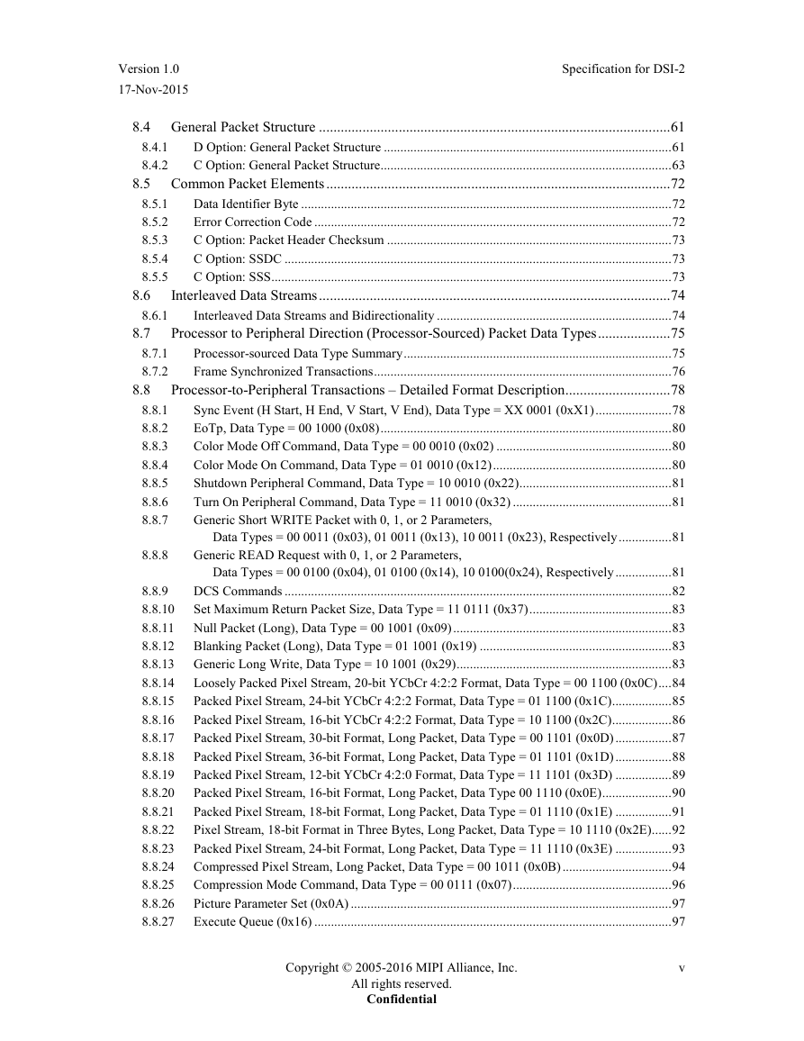
8.4 General Packet Structure
8.4.1 D Option: General Packet Structure
8.4.1.1 D-PHY Long Packet Format
8.4.1.2 D-PHY Short Packet Format
8.4.2 C Option: General Packet Structure
8.4.2.1 C-PHY Long Packet Format in High Speed Mode
8.4.2.2 C-PHY Short Packet Format in High Speed Mode
8.4.2.3 C-PHY Long Packet Format in Escape Mode
8.4.2.4 C-PHY Short Packet Format in Escape Mode
8.5 Common Packet Elements
8.5.1 Data Identifier Byte
8.5.1.1 Virtual Channel Identifier – VC field, DI[7:6]
8.5.1.2 Data Type Field DT[5:0]
8.5.2 Error Correction Code
8.5.3 C Option: Packet Header Checksum
8.5.4 C Option: SSDC
8.5.5 C Option: SSS
8.6 Interleaved Data Streams
8.6.1 Interleaved Data Streams and Bidirectionality
8.7 Processor to Peripheral Direction (Processor-Sourced) Packet Data Types
8.7.1 Processor-sourced Data Type Summary
8.7.2 Frame Synchronized Transactions
8.8 Processor-to-Peripheral Transactions – Detailed Format Description
8.8.1 Sync Event (H Start, H End, V Start, V End), Data Type = XX 0001 (0xX1)
8.8.1.1 Sync Event Payloads
8.8.1.2 Stereoscopic Display Control in Video Mode (3D Control)
8.8.2 EoTp, Data Type = 00 1000 (0x08)
8.8.3 Color Mode Off Command, Data Type = 00 0010 (0x02)
8.8.4 Color Mode On Command, Data Type = 01 0010 (0x12)
8.8.5 Shutdown Peripheral Command, Data Type = 10 0010 (0x22)
8.8.6 Turn On Peripheral Command, Data Type = 11 0010 (0x32)
8.8.7 Generic Short WRITE Packet with 0, 1, or 2 Parameters, Data Types = 00 0011 (0x03), 01 0011 (0x13), 10 0011 (0x23), Respectively
8.8.8 Generic READ Request with 0, 1, or 2 Parameters, Data Types = 00 0100 (0x04), 01 0100 (0x14), 10 0100(0x24), Respectively
8.8.9 DCS Commands
8.8.9.1 DCS Short Write Command, 0 or 1 Parameter, Data Types = 00 0101 (0x05), 01 0101 (0x15), Respectively
8.8.9.2 DCS Read Request, No Parameters, Data Type = 00 0110 (0x06)
8.8.9.3 DCS Long Write / write_LUT Command, Data Type = 11 1001 (0x39)
8.8.10 Set Maximum Return Packet Size, Data Type = 11 0111 (0x37)
8.8.11 Null Packet (Long), Data Type = 00 1001 (0x09)
8.8.12 Blanking Packet (Long), Data Type = 01 1001 (0x19)
8.8.13 Generic Long Write, Data Type = 10 1001 (0x29)
8.8.14 Loosely Packed Pixel Stream, 20-bit YCbCr 4:2:2 Format, Data Type = 00 1100 (0x0C)
8.8.15 Packed Pixel Stream, 24-bit YCbCr 4:2:2 Format, Data Type = 01 1100 (0x1C)
8.8.16 Packed Pixel Stream, 16-bit YCbCr 4:2:2 Format, Data Type = 10 1100 (0x2C)
8.8.17 Packed Pixel Stream, 30-bit Format, Long Packet, Data Type = 00 1101 (0x0D)
8.8.18 Packed Pixel Stream, 36-bit Format, Long Packet, Data Type = 01 1101 (0x1D)
8.8.19 Packed Pixel Stream, 12-bit YCbCr 4:2:0 Format, Data Type = 11 1101 (0x3D)
8.8.20 Packed Pixel Stream, 16-bit Format, Long Packet, Data Type 00 1110 (0x0E)
8.8.21 Packed Pixel Stream, 18-bit Format, Long Packet, Data Type = 01 1110 (0x1E)
8.8.22 Pixel Stream, 18-bit Format in Three Bytes, Long Packet, Data Type = 10 1110 (0x2E)
8.8.23 Packed Pixel Stream, 24-bit Format, Long Packet, Data Type = 11 1110 (0x3E)
8.8.24 Compressed Pixel Stream, Long Packet, Data Type = 00 1011 (0x0B)
8.8.25 Compression Mode Command, Data Type = 00 0111 (0x07)
8.8.26 Picture Parameter Set (0x0A)
8.8.27 Execute Queue (0x16)
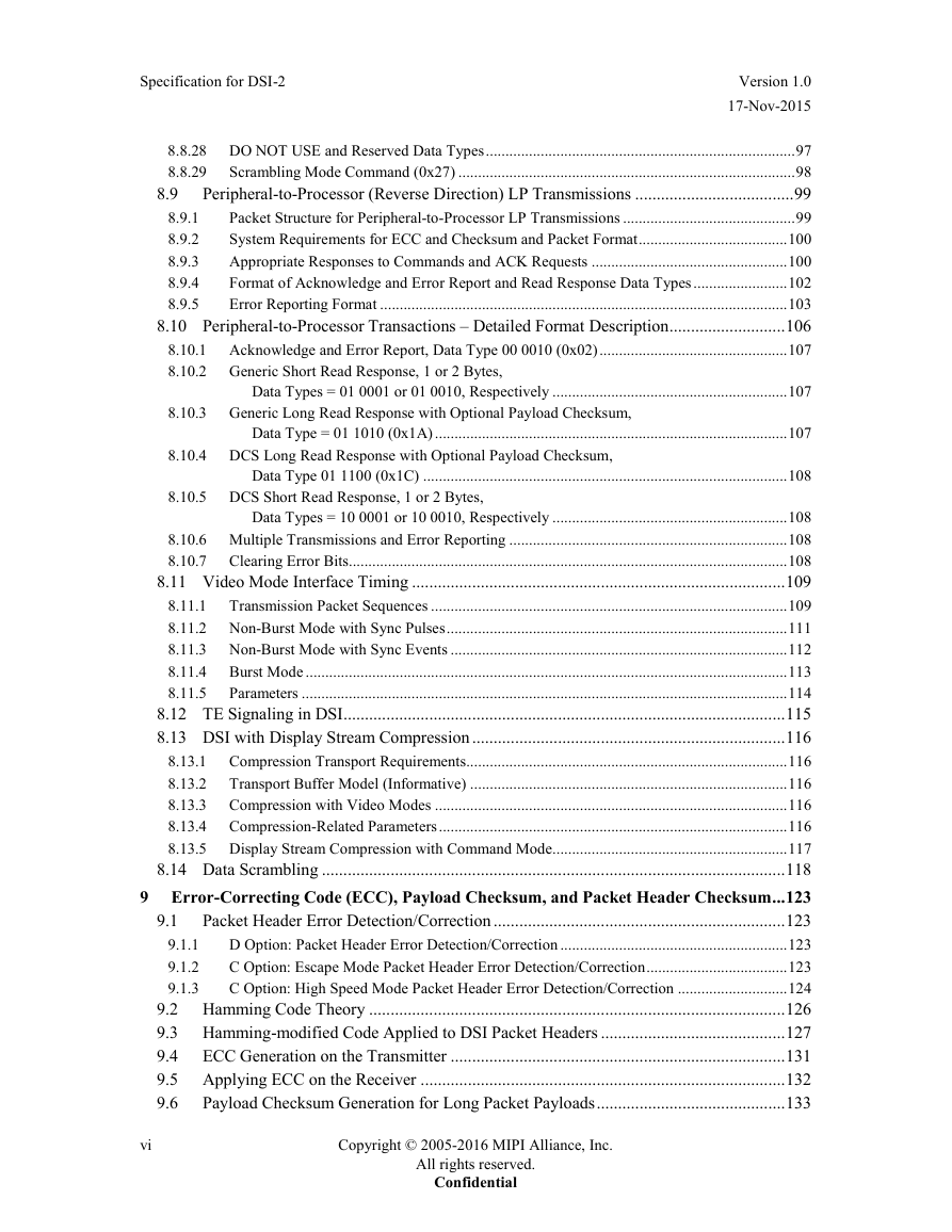
8.8.28 DO NOT USE and Reserved Data Types
8.8.29 Scrambling Mode Command (0x27)
8.9 Peripheral-to-Processor (Reverse Direction) LP Transmissions
8.9.1 Packet Structure for Peripheral-to-Processor LP Transmissions
8.9.2 System Requirements for ECC and Checksum and Packet Format
8.9.3 Appropriate Responses to Commands and ACK Requests
8.9.4 Format of Acknowledge and Error Report and Read Response Data Types
8.9.5 Error Reporting Format
8.9.5.1 D Option: Error Reporting Format
8.9.5.2 C Option: Error Reporting Format
8.10 Peripheral-to-Processor Transactions – Detailed Format Description
8.10.1 Acknowledge and Error Report, Data Type 00 0010 (0x02)
8.10.2 Generic Short Read Response, 1 or 2 Bytes, Data Types = 01 0001 or 01 0010, Respectively
8.10.3 Generic Long Read Response with Optional Payload Checksum, Data Type = 01 1010 (0x1A)
8.10.4 DCS Long Read Response with Optional Payload Checksum, Data Type 01 1100 (0x1C)
8.10.5 DCS Short Read Response, 1 or 2 Bytes, Data Types = 10 0001 or 10 0010, Respectively
8.10.6 Multiple Transmissions and Error Reporting
8.10.7 Clearing Error Bits
8.11 Video Mode Interface Timing
8.11.1 Transmission Packet Sequences
8.11.2 Non-Burst Mode with Sync Pulses
8.11.3 Non-Burst Mode with Sync Events
8.11.4 Burst Mode
8.11.5 Parameters
8.12 TE Signaling in DSI
8.13 DSI with Display Stream Compression
8.13.1 Compression Transport Requirements
8.13.2 Transport Buffer Model (Informative)
8.13.3 Compression with Video Modes
8.13.4 Compression-Related Parameters
8.13.5 Display Stream Compression with Command Mode
8.14 Data Scrambling
9 Error-Correcting Code (ECC), Payload Checksum, and Packet Header Checksum
9.1 Packet Header Error Detection/Correction
9.1.1 D Option: Packet Header Error Detection/Correction
9.1.2 C Option: Escape Mode Packet Header Error Detection/Correction
9.1.3 C Option: High Speed Mode Packet Header Error Detection/Correction
9.2 Hamming Code Theory
9.3 Hamming-Modified Code Applied to DSI Packet Headers
9.4 ECC Generation on the Transmitter
9.5 Applying ECC on the Receiver
9.6 Payload Checksum Generation for Long Packet Payloads
9.7 Checksum Generation for Reconstructed Image Test Mode
10 Compliance, Interoperability, and Optional Capabilities
10.1 Display Resolutions
10.2 Pixel Formats
10.2.1 Video Mode
10.2.2 Command Mode
10.3 Number of Lanes
10.4 Maximum Lane Frequency
10.5 Bidirectional Communication
10.6 ECC and Checksum Capabilities
10.6.1 D Option: ECC and Checksum Capabilities
10.6.2 C Option: SSDC, ECC, and Checksum Capabilities
10.7 Display Architecture
10.8 Multiple Peripheral Support
10.9 EoTp Support and Interoperability
Annex A Contention Detection and Recovery Mechanisms (Informative)
A.1 PHY Detected Contention
A.1.1 Protocol Response to PHY Detected Faults
Annex B Checksum Generation Examples (Informative)
B.1 Payload Checksum Generation Example
B.2 C-PHY Packet Header Checksum Example
Annex C Interlaced Video Transmission Sourcing
Annex D Profile for DSI Transport for VESA Display Stream Compression
D.1 Profile Normative Requirements
D.1.1 Encoder Instantiations
D.1.2 Decoder Instantiations
D.1.3 Horizontal Slice Size
D.1.4 Vertical Slice Size
D.1.5 DSC Parameter Minimum Requirements
D.1.6 PPS Requirements
D.2 Implementation Guidelines (Informative)
D.2.1 Vertical Slice Size
D.2.2 DSC Guidelines
Annex E Differences Between DSI-2 Devices Supporting D-PHY and C-PHY (Informative)
Annex F Continuous Clock Mode Support With C-PHY




 2023年江西萍乡中考道德与法治真题及答案.doc
 2012年重庆南川中考生物真题及答案.doc
 2013年江西师范大学地理学综合及文艺理论基础考研真题.doc
 2020年四川甘孜小升初语文真题及答案I卷.doc
 2020年注册岩土工程师专业基础考试真题及答案.doc
 2023-2024学年福建省厦门市九年级上学期数学月考试题及答案.doc
 2021-2022学年辽宁省沈阳市大东区九年级上学期语文期末试题及答案.doc
 2022-2023学年北京东城区初三第一学期物理期末试卷及答案.doc
 2018上半年江西教师资格初中地理学科知识与教学能力真题及答案.doc
 2012年河北国家公务员申论考试真题及答案-省级.doc
 2020-2021学年江苏省扬州市江都区邵樊片九年级上学期数学第一次质量检测试题及答案.doc
 2022下半年黑龙江教师资格证中学综合素质真题及答案.doc