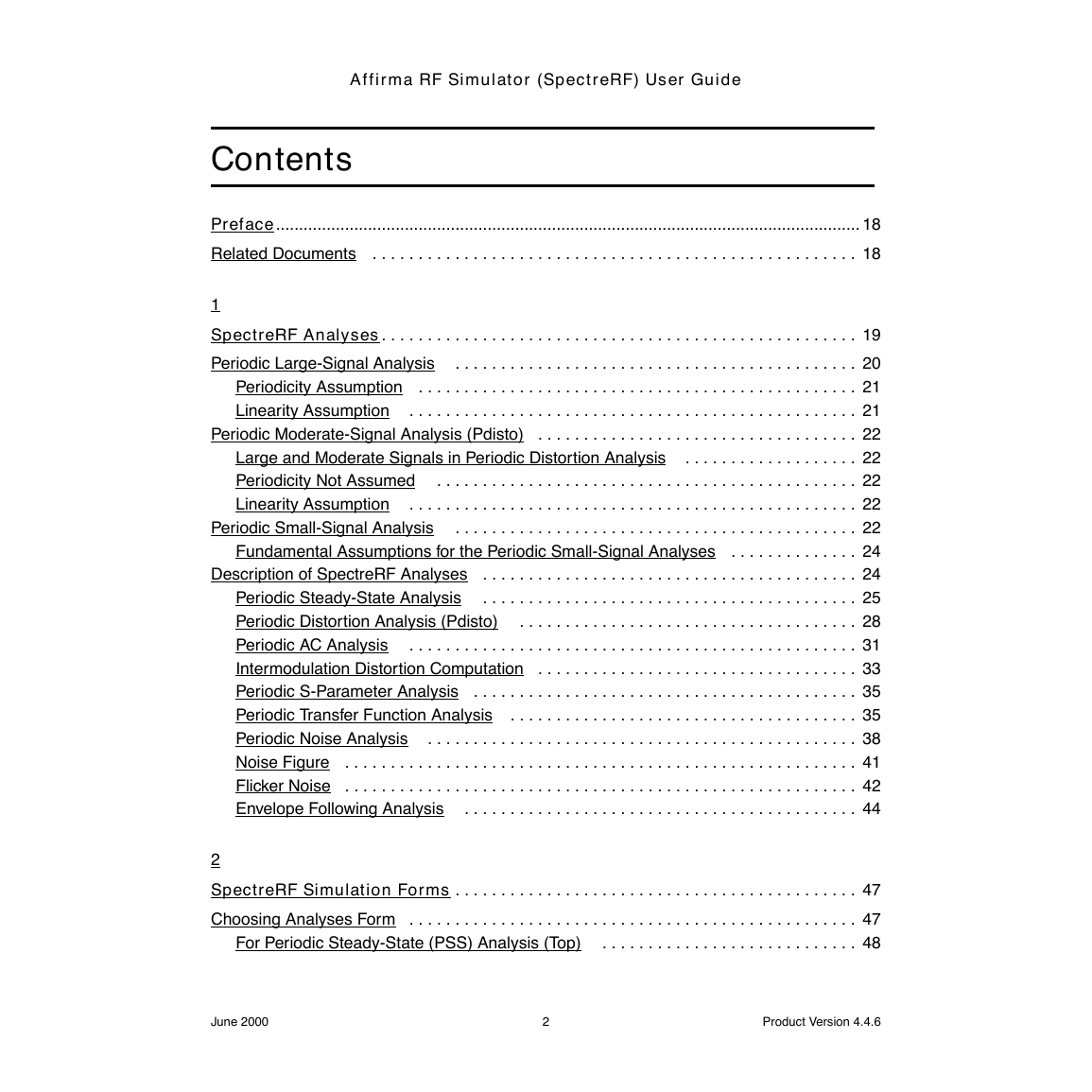
Contents
Preface
Related Documents
SpectreRF Analyses
Periodic Large-Signal Analysis
Periodicity Assumption
Linearity Assumption
Periodic Moderate-Signal Analysis (Pdisto)
Large and Moderate Signals in Periodic Distortion Analysis
Periodicity Not Assumed
Linearity Assumption
Periodic Small-Signal Analysis
Fundamental Assumptions for the Periodic Small-Signal Analyses
Description of SpectreRF Analyses
Periodic Steady-State Analysis
Periodic Distortion Analysis (Pdisto)
Periodic AC Analysis
Intermodulation Distortion Computation
Periodic S-Parameter Analysis
Periodic Transfer Function Analysis
Periodic Noise Analysis
Noise Figure
Flicker Noise
Envelope Following Analysis
SpectreRF Simulation Forms
Choosing Analyses Form
For Periodic Steady-State (PSS) Analysis (Top)
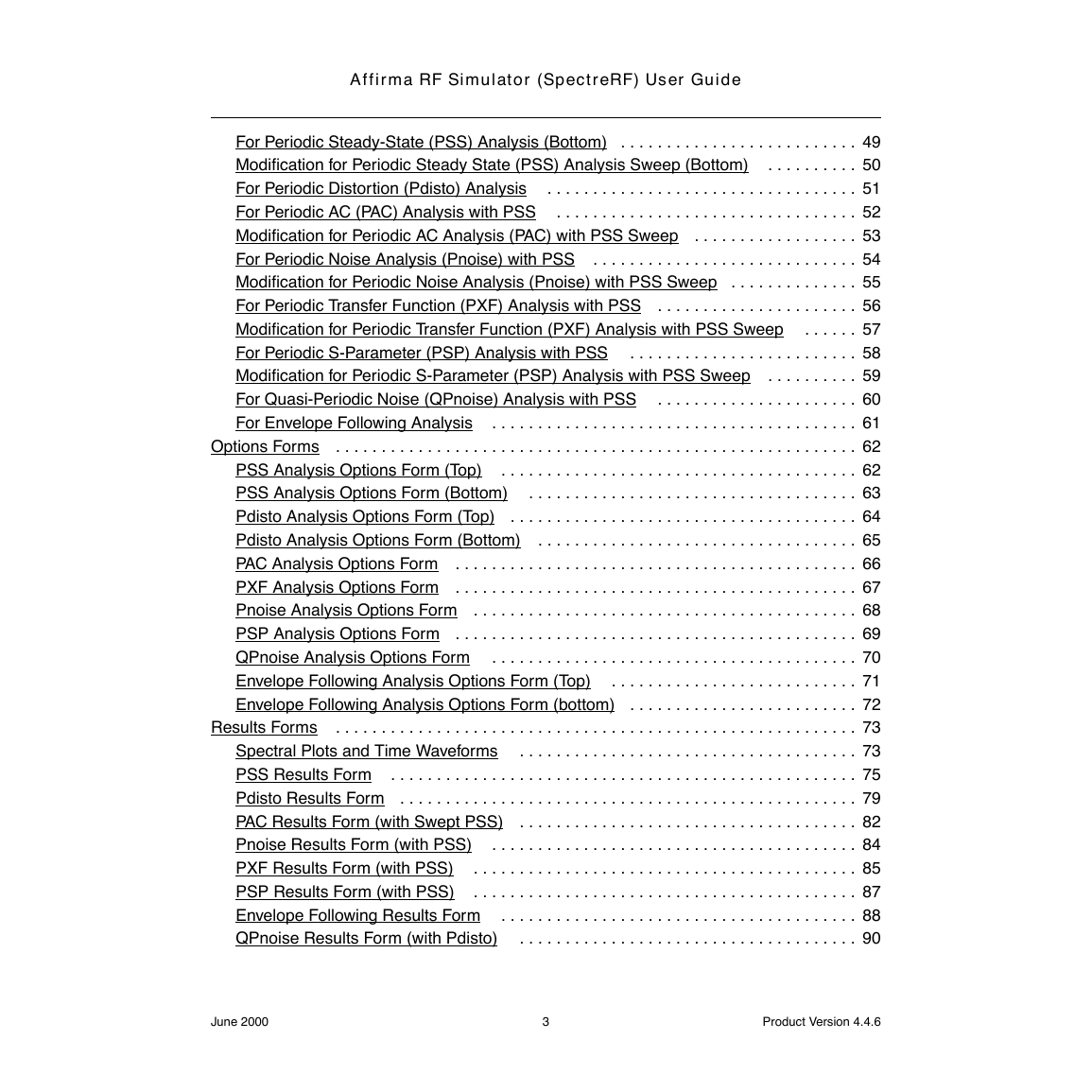
For Periodic Steady-State (PSS) Analysis (Bottom)
Modification for Periodic Steady State (PSS) Analysis Sweep (Bottom)
For Periodic Distortion (Pdisto) Analysis
For Periodic AC (PAC) Analysis with PSS
Modification for Periodic AC Analysis (PAC) with PSS Sweep
For Periodic Noise Analysis (Pnoise) with PSS
Modification for Periodic Noise Analysis (Pnoise) with PSS Sweep
For Periodic Transfer Function (PXF) Analysis with PSS
Modification for Periodic Transfer Function (PXF) Analysis with PSS Sweep
For Periodic S-Parameter (PSP) Analysis with PSS
Modification for Periodic S-Parameter (PSP) Analysis with PSS Sweep
For Quasi-Periodic Noise (QPnoise) Analysis with PSS
For Envelope Following Analysis
Options Forms
PSS Analysis Options Form (Top)
PSS Analysis Options Form (Bottom)
Pdisto Analysis Options Form (Top)
Pdisto Analysis Options Form (Bottom)
PAC Analysis Options Form
PXF Analysis Options Form
Pnoise Analysis Options Form
PSP Analysis Options Form
QPnoise Analysis Options Form
Envelope Following Analysis Options Form (Top)
Envelope Following Analysis Options Form (bottom)
Results Forms
Spectral Plots and Time Waveforms
PSS Results Form
Pdisto Results Form
PAC Results Form (with Swept PSS)
Pnoise Results Form (with PSS)
PXF Results Form (with PSS)
PSP Results Form (with PSS)
Envelope Following Results Form
QPnoise Results Form (with Pdisto)
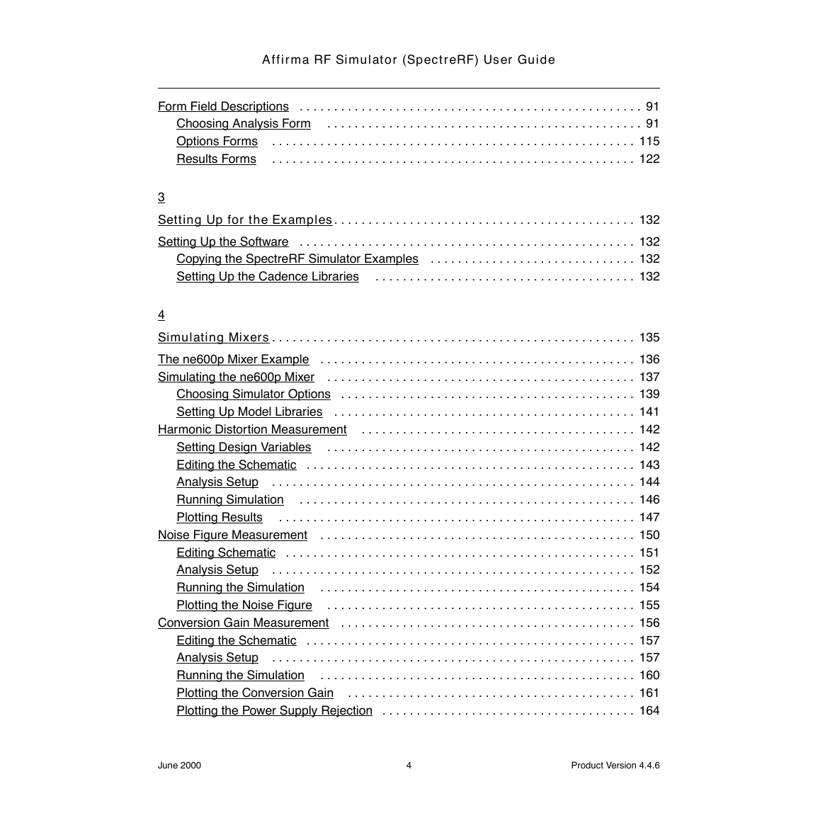
Form Field Descriptions
Choosing Analysis Form
Options Forms
Results Forms
Setting Up for the Examples
Setting Up the Software
Copying the SpectreRF Simulator Examples
Setting Up the Cadence Libraries
Simulating Mixers
The ne600p Mixer Example
Simulating the ne600p Mixer
Choosing Simulator Options
Setting Up Model Libraries
Harmonic Distortion Measurement
Setting Design Variables
Editing the Schematic
Analysis Setup
Running Simulation
Plotting Results
Noise Figure Measurement
Editing Schematic
Analysis Setup
Running the Simulation
Plotting the Noise Figure
Conversion Gain Measurement
Editing the Schematic
Analysis Setup
Running the Simulation
Plotting the Conversion Gain
Plotting the Power Supply Rejection
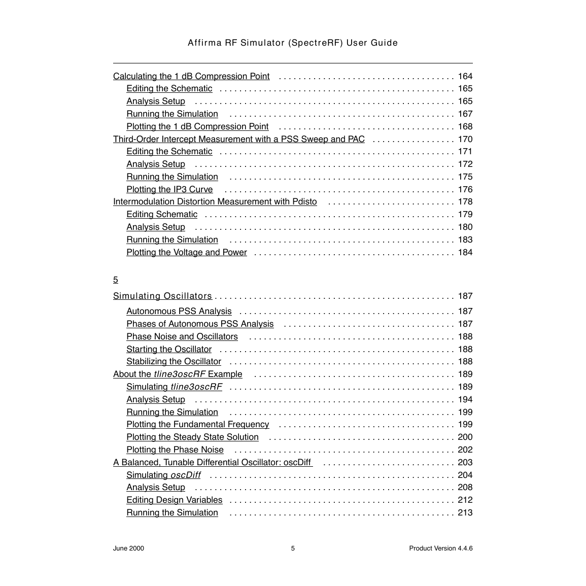
Calculating the 1 dB Compression Point
Editing the Schematic
Analysis Setup
Running the Simulation
Plotting the 1 dB Compression Point
Third-Order Intercept Measurement with a PSS Sweep and PAC
Editing the Schematic
Analysis Setup
Running the Simulation
Plotting the IP3 Curve
Intermodulation Distortion Measurement with Pdisto
Editing Schematic
Analysis Setup
Running the Simulation
Plotting the Voltage and Power
Simulating Oscillators
Autonomous PSS Analysis
Phases of Autonomous PSS Analysis
Phase Noise and Oscillators
Starting the Oscillator
Stabilizing the Oscillator
About the tline3oscRF Example
Simulating tline3oscRF
Analysis Setup
Running the Simulation
Plotting the Fundamental Frequency
Plotting the Steady State Solution
Plotting the Phase Noise
A Balanced, Tunable Differential Oscillator: oscDiff
Simulating oscDiff
Analysis Setup
Editing Design Variables
Running the Simulation
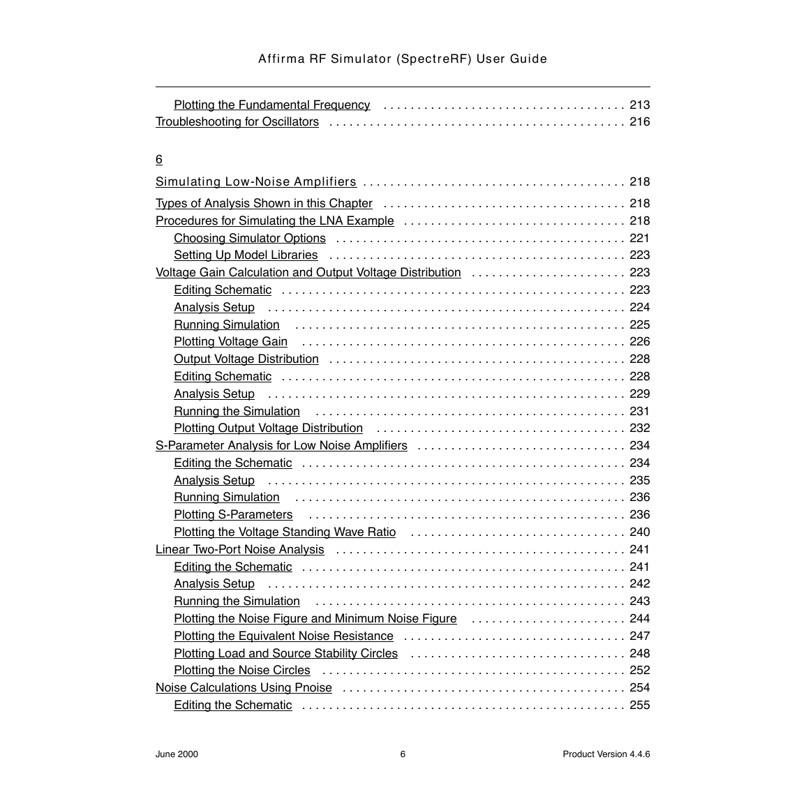
Plotting the Fundamental Frequency
Troubleshooting for Oscillators
Simulating Low-Noise Amplifiers
Types of Analysis Shown in this Chapter
Procedures for Simulating the LNA Example
Choosing Simulator Options
Setting Up Model Libraries
Voltage Gain Calculation and Output Voltage Distribution
Editing Schematic
Analysis Setup
Running Simulation
Plotting Voltage Gain
Output Voltage Distribution
Editing Schematic
Analysis Setup
Running the Simulation
Plotting Output Voltage Distribution
S-Parameter Analysis for Low Noise Amplifiers
Editing the Schematic
Analysis Setup
Running Simulation
Plotting S-Parameters
Plotting the Voltage Standing Wave Ratio
Linear Two-Port Noise Analysis
Editing the Schematic
Analysis Setup
Running the Simulation
Plotting the Noise Figure and Minimum Noise Figure
Plotting the Equivalent Noise Resistance
Plotting Load and Source Stability Circles
Plotting the Noise Circles
Noise Calculations Using Pnoise
Editing the Schematic
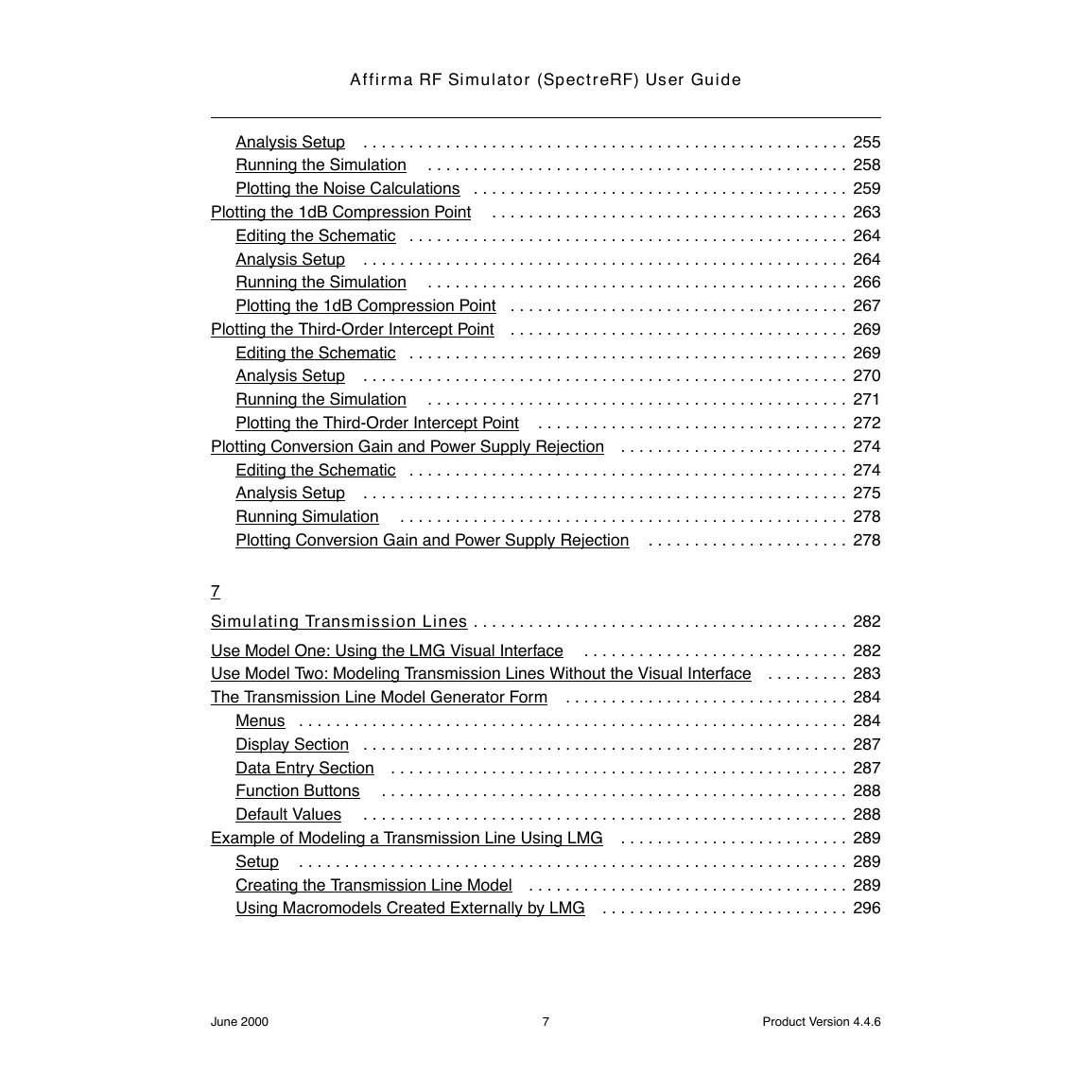
Analysis Setup
Running the Simulation
Plotting the Noise Calculations
Plotting the 1dB Compression Point
Editing the Schematic
Analysis Setup
Running the Simulation
Plotting the 1dB Compression Point
Plotting the Third-Order Intercept Point
Editing the Schematic
Analysis Setup
Running the Simulation
Plotting the Third-Order Intercept Point
Plotting Conversion Gain and Power Supply Rejection
Editing the Schematic
Analysis Setup
Running Simulation
Plotting Conversion Gain and Power Supply Rejection
Simulating Transmission Lines
Use Model One: Using the LMG Visual Interface
Use Model Two: Modeling Transmission Lines Without the Visual Interface
The Transmission Line Model Generator Form
Menus
Display Section
Data Entry Section
Function Buttons
Default Values
Example of Modeling a Transmission Line Using LMG
Setup
Creating the Transmission Line Model
Using Macromodels Created Externally by LMG
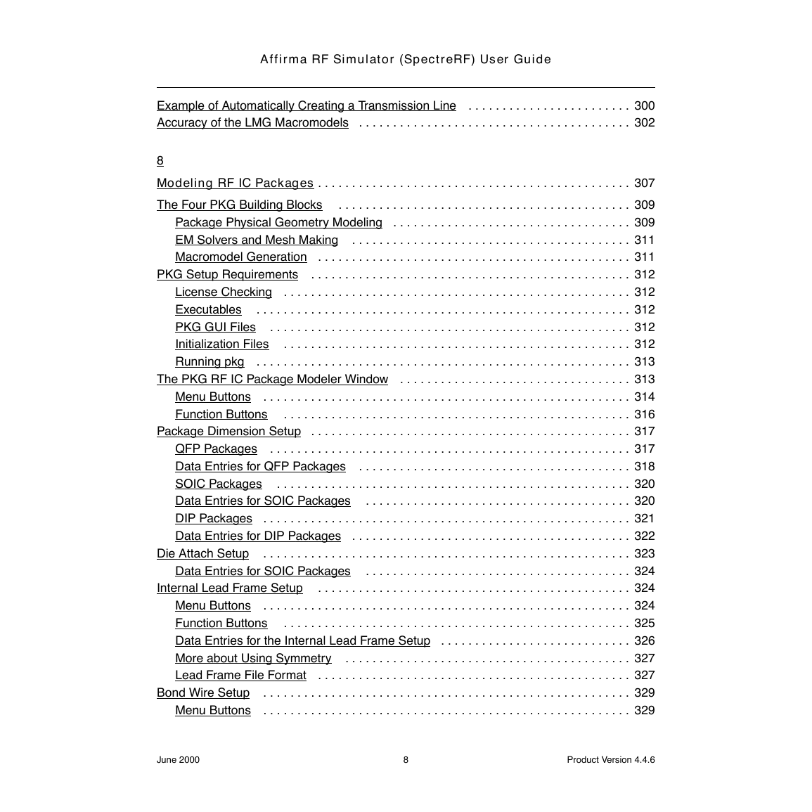
Example of Automatically Creating a Transmission Line
Accuracy of the LMG Macromodels
Modeling RF IC Packages
The Four PKG Building Blocks
Package Physical Geometry Modeling
EM Solvers and Mesh Making
Macromodel Generation
PKG Setup Requirements
License Checking
Executables
PKG GUI Files
Initialization Files
Running pkg
The PKG RF IC Package Modeler Window
Menu Buttons
Function Buttons
Package Dimension Setup
QFP Packages
Data Entries for QFP Packages
SOIC Packages
Data Entries for SOIC Packages
DIP Packages
Data Entries for DIP Packages
Die Attach Setup
Data Entries for SOIC Packages
Internal Lead Frame Setup
Menu Buttons
Function Buttons
Data Entries for the Internal Lead Frame Setup
More about Using Symmetry
Lead Frame File Format
Bond Wire Setup
Menu Buttons
Function Buttons
Data Entries for the Bond Wire Setup
Bond Wire Configurations
Bond Wire File Format
Save the Current Setting
Parameter Extraction
Capacitance Calculation
Inductance Calculation
Function Buttons for Parameter Extraction
Macromodel Generation
Data Entries and Buttons for Macromodel Generation
Die Attach Terminal
Macromodel Schematic
High Frequency Resonance Damping for the Spectre Simulator
Accuracy Analysis
Simulation of Package Models in the Affirma Analog Circuit Design Environment
Example of Package Modeling With a Mixer Using PKG
Extracting K-Models
Procedures for Simulating k_mod_extraction_example
Analysis Setup
Running the Simulation
Checking the Simulation Results
Creating the K-Model
More About the K-Model
K-model data files
Extracting J-Models
Procedures for Simulating j_mod_extraction_example
Analysis Setup
Running the Simulation
Creating the J-Model
Using the J-model in a circuit
More About the J-model
Modeling Transmitters
Envelope Following
Taking a Closer Look at the Envelope Following Procedure
Following the Change in the Information (Baseband Signal) Through the Circuit
Plotting the Complete Baseband Signal
Plotting the Baseband Trajectory
Plotting the Transmitted Power Spectral Density for ACPR Calculations
Measuring Load Pull Contours and Reflection Coefficients
Setting Up and Running the Simulation
Displaying Load Contours
Adding the Reflection Contours to the Plot
Let’s assume that for stability, the input reflection coefficient should be less than or equal to...
Moving to Differential Mode
Using S-Parameter Input Files
Setting Up the Schematic for the First Simulation
Setting Up and Running the First Simulation
The S-Parameter File
Setting Up and Running the Second Simulation
Using an S-Parameter Input File with a SpectreRF Analysis
Modeling Spiral Inductors and Bondpads
Modeling Spiral Inductors
Process File Preparation
Spiral Inductor Simulation in the Schematic Flow
Spiral Inductor Modeling under the RF Sub-Menu
Equivalent Circuit Models
Example
Modeling Bondpads
Input to the Modeler
Parameter Sets
Modeling Issues
LNA Example
References for the Bondpad Section
Behavioral Models and Methods for Top Down Design
Top Down Design of RF Systems
Baseband Modeling
Plotting Baseband Equivalent Output Signals for Baseband and Passband Circuits
About Baseband Modeling
Library Overview
Warnings You Can Ignore
Use Model and Design Example
Relationship Between Baseband and Passband Noise
Baseband Library
Assumptions
Compatibility
Library Categories
Inputs and Outputs on Baseband Models
Some Parameters Common to Several Models
Library Description
Notes on models involving frequency translation:
Power Amplifier Model
Low Noise Amplifier Baseband Model
IQ Modulator Models
IQ Demodulator
RF-to-IFand IF-to-RF Mixers
Passive Devices
Linear Time Invariant Filters
Comparison of baseband and passband models
BB_Loss
Phase Shifter
Phase Shifter
Ideal Transformer
Rectangular-to-Polar Transformation
Polar-to-Rectangular Transformation
Instrumentation and Terminating Blocks
Baseband Drive Signals
References
Oscillator Noise Analysis
Phase Noise Primer
Models for Phase Noise
Linear Time-Invariant (LTI) Models
Linear Time-Varying (LTV) Models
Amplitude Noise and Phase Noise in the “Linear” Model
Details of the SpectreRF Calculation
Calculating Phase Noise
Setting Simulator Options
Tips about Getting PSS to Converge
How to Tell If the Answer Is Correct
Troubleshooting Phase Noise Calculations
Known Limitations of the Simulator
What Can Go Wrong
Phase Noise Error Messages
The tstab Parameter
Frequently Asked Questions
Further Reading
References
Running PSS Effectively
General Convergence Aids
Convergence Aids for Oscillators
Running PSS Hierarchically
Using the psin Component
Independent Resistive Source (psin)
Parameter Types for the psin Component
Name Parameters
psin Instance Parameter
General Waveform Parameters
Sinusoidal Waveform Parameters
Amplitude Modulation Parameters
FM Modulation Parameters
Noise Parameters
Port Parameters
Temperature Effect Parameters
Small-Signal Parameters
Additional Notes
The RF Library
Top-Down Design Elements
Filter
Balun
Low Noise Amplifier
Mixer
Power Amplifier
Oscillator
Quadrature Signal Generator
Phase Shifter
Bottom-Up Design Elements
Testbench Elements
CDMA Signal Source (IS-95 rev_xmit) and Eye-Diagram Generator
GSM Signal Source (GSM-xmtr)
P/4-DQPSK Signal Source (pi_over4_dqpsk)
Creating Variations on the Library Baseband Signal Generators Using the Modelwriter
Uncatagorized Elements
Plotting Spectre S-Parameter Simulation Data
The Equations for the S-Parameter Waveform Calculator in the Affirma Analog Circuit Design Enviro...
Using PDisto Effectively
When to Use PDisto
Essentials of the MFT Method
PDisto compared with PSS
PDisto Compared with PAC
PDisto Analysis Parameters
Application Examples
Using PDisto
Sweeping PDisto
Convergence Aids
References
An Introduction to the PLL library
The Models in the PLL library
Introduction
Phase-Domain Model of a Simple PLL
Assembling a Model of a PFD-based PLL
How the PFD Model Works.
References
Using port in SpectreRF Simulations
port Parameter Types
Port Parameters
General Waveform Parameters
DC Waveform Parameters
Pulse Waveform Parameters
PWL Waveform Parameters
Sinusoidal Waveform Parameters
Exponential Waveform Parameters
Noise Parameters
Small-Signal Parameters
Temperature Effect Parameters
Additional Notes
Analyzing Time-Varying Noise Properties
Time-Domain Noise Characterization
Calculating Noise Correlation Coefficients
Using Tabulated S-parameters
Using the nport component
Controlling Model Accuracy
Using relerr and abserr
Using the ratorder parameter
Troubleshooting
Assessing the quality of the rational interpolation
Model Reuse
References
Using the Calculator IPN Functions for RF Simulations
How to Use the ipn and ipnVRI Functions
Setting Up
Editing the Schematic
Setting Up the Analysis
Running the Simulation
Plotting the IP3 Curve Using Direct Plot
Plot IP3 Using the ipn and ipnVRI Buttons in the Waveform Calculator
Using the IPN Function with Scalar Inputs
Setting Up
Setting Up the Analysis
Running Simulation
Plotting the Single Point IP3 Using the Calculator
Using PSP and Pnoise Analyses
Overview
Periodic S-parameters
Linear Time-Invariant S-Parameters
Frequency Translating S-Parameters
Upper and Lower Sidebands
Example
Noise and Noise Parameters
Calculating Noise in Linear Time-Invariant (DC Bias) Circuits
Calculating Noise in Time-Varying (Periodic Bias) Circuits
The maxsideband Parameter
Noise Correlation Matrices and Equivalent Noise Sources
Noise Figure
Performing Noise Figure Computations
Noise Figure From Noise and SP Analyses
Pnoise (SSB) Noise Figure
DSB Noise Figure
IEEE Noise Figure
Example
Input Referred Noise
Using IRN
How IRN is Calculated
Relation to Gain
Referring Noise to Ports
Gain calculations
Definitions of Gain
Gain Calculations in Pnoise
Phase Noise
Frequently Asked Questions
Known Problems and Limitations
Dubious AC-Noise Analysis Features
Gain in Pnoise and PSP Analyses Inconsistent
Harmonics and Sidebands in PSP, PAC, PXF, And Pnoise Analyses
Index


 2023年江西萍乡中考道德与法治真题及答案.doc
 2012年重庆南川中考生物真题及答案.doc
 2013年江西师范大学地理学综合及文艺理论基础考研真题.doc
 2020年四川甘孜小升初语文真题及答案I卷.doc
 2020年注册岩土工程师专业基础考试真题及答案.doc
 2023-2024学年福建省厦门市九年级上学期数学月考试题及答案.doc
 2021-2022学年辽宁省沈阳市大东区九年级上学期语文期末试题及答案.doc
 2022-2023学年北京东城区初三第一学期物理期末试卷及答案.doc
 2018上半年江西教师资格初中地理学科知识与教学能力真题及答案.doc
 2012年河北国家公务员申论考试真题及答案-省级.doc
 2020-2021学年江苏省扬州市江都区邵樊片九年级上学期数学第一次质量检测试题及答案.doc
 2022下半年黑龙江教师资格证中学综合素质真题及答案.doc