LM3478 High-Efficiency Low-Side N-Channel Controller for Switching Regulator
LM3478
SNVS085X –JULY 2000–REVISED DECEMBER 2017
1 Features
1• 8-lead VSSOP-8 and SOIC-8 packages
•
Internal Push-Pull Driver With 1-A Peak Current
Capability
• Current Limit and Thermal Shutdown
• Frequency Compensation Optimized With a
Capacitor and a Resistor
Internal Soft Start
•
• Current Mode Operation
• Undervoltage Lockout With Hysteresis
• Create a Custom Design Using the LM3478 with
the WEBENCH Power Designer
2 Applications
• Distributed Power Systems
• Battery Chargers
• Offline Power Supplies
• Telecom Power Supplies
• Automotive Power Systems
• Wide Supply Voltage Range of 2.97 V to 40 V
100-kHz to 1-MHz Adjustable Clock Frequency
•
±2.5% (Over Temperature) Internal Reference
•
•
10-µA Shutdown Current (Over Temperature)
It
for switching regulators.
3 Description
The LM3478 is a versatile Low-Side N-Channel
MOSFET controller
is
suitable for use in topologies requiring a low side
MOSFET, such as boost,
flyback, SEPIC, etc.
Moreover, the LM3478 can be operated at extremely
high switching frequency in order
to reduce the
overall solution size. The switching frequency of the
LM3478 can be adjusted to any value between 100
kHz and 1 MHz by using a single external resistor.
Current mode control provides superior bandwidth
and transient
cycle-by-cycle
current limiting. Output current can be programmed
with a single external resistor.
The LM3478 has built-in features such as thermal
shutdown,
voltage
protection, etc. Power
saving shutdown mode
reduces the total supply current to 5 µA and allows
power supply sequencing. Internal soft-start limits the
inrush current at start-up.
short-circuit protection, over
response, besides
Device Information(1)
LM3478
PACKAGE
PART NUMBER
BODY SIZE (NOM)
4.90 mm x 3.91 mm
3.00 mm x 3.00 mm
(1) For all available packages, see the orderable addendum at
SOIC (8)
VSSOP (8)
the end of the datasheet.
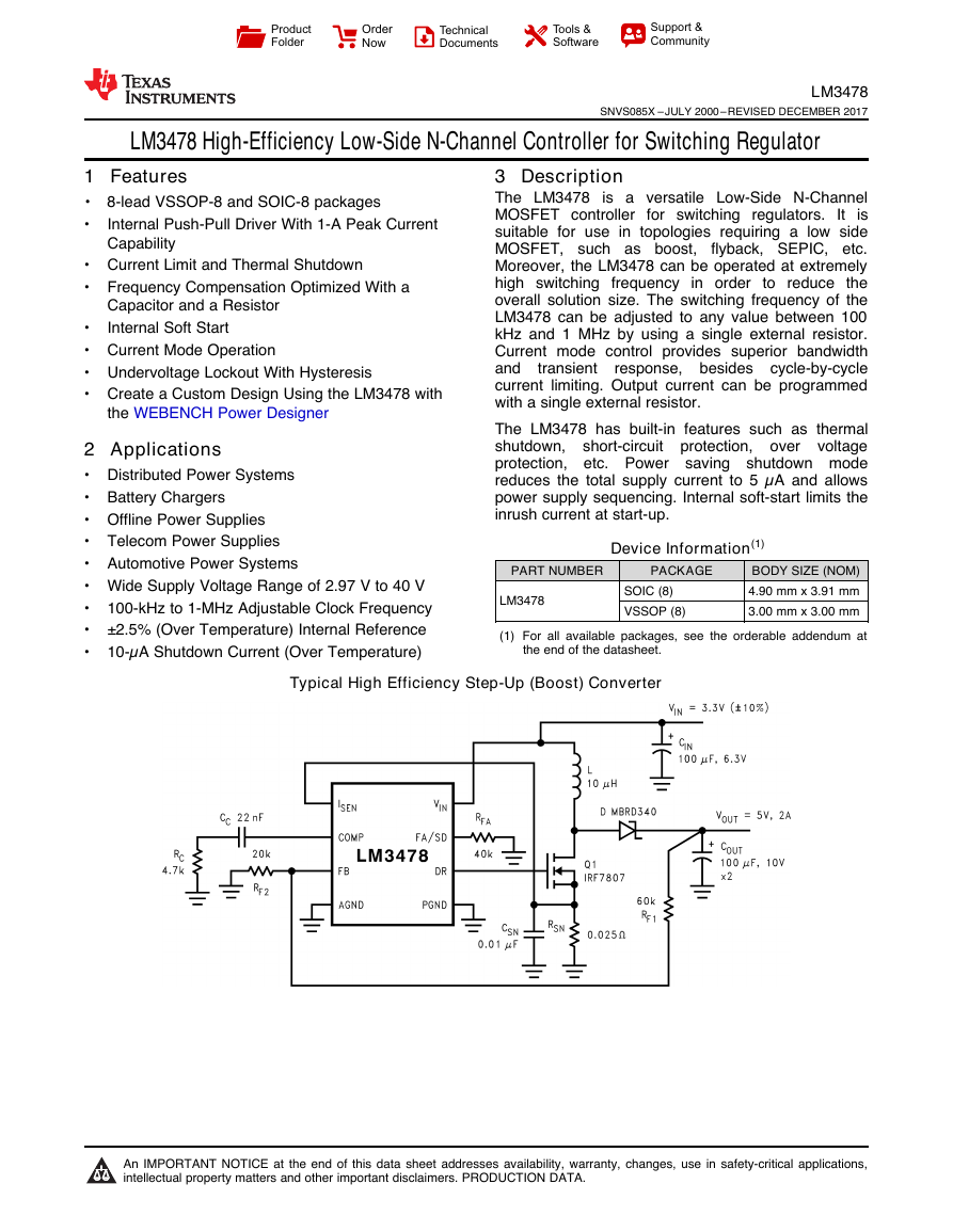
Typical High Efficiency Step-Up (Boost) Converter
1
An IMPORTANT NOTICE at the end of this data sheet addresses availability, warranty, changes, use in safety-critical applications,
intellectual property matters and other important disclaimers. PRODUCTION DATA.
ProductFolderOrderNowTechnicalDocumentsTools &SoftwareSupport &Community�
LM3478
SNVS085X –JULY 2000–REVISED DECEMBER 2017
www.ti.com
Table of Contents
1
Features.................................................................. 1
2 Applications ........................................................... 1
3 Description ............................................................. 1
4 Revision History..................................................... 2
5 Pin Configuration and Functions ......................... 3
6 Specifications......................................................... 4
6.1 Absolute Maximum Ratings ...................................... 4
6.2 ESD Ratings - LM3478 ............................................ 4
6.3 Recommended Operating Conditions....................... 4
6.4 Thermal Information.................................................. 5
6.5 Electrical Characteristics........................................... 5
6.6 Typical Characteristics.............................................. 7
7 Detailed Description ............................................ 11
7.1 Overview ................................................................. 11
7.2 Functional Block Diagram ....................................... 12
7.3 Feature Description................................................. 12
7.4 Device Functional Modes........................................ 15
8 Application and Implementation ........................ 16
8.1 Application Information............................................ 16
8.2 Typical Applications ................................................ 16
9 Power Supply Recommendations...................... 28
10 Layout................................................................... 28
10.1 Layout Guidelines ................................................. 28
10.2 Layout Example .................................................... 29
11 Device and Documentation Support ................. 30
11.1 Custom Design with WEBENCH Tools................. 30
11.2 Receiving Notification of Documentation Updates 30
11.3 Documentation Support ....................................... 30
11.4 Related Links ........................................................ 30
11.5 Trademarks ........................................................... 30
11.6 Electrostatic Discharge Caution............................ 30
11.7 Glossary ................................................................ 30
12 Mechanical, Packaging, and Orderable
Information ........................................................... 31
4 Revision History
NOTE: Page numbers for previous revisions may differ from page numbers in the current version.
Changes from Revision W (December 2014) to Revision X
Page
• Deleted LM3478Q-Q1 device. See LM3478Q-Q1 data sheet ............................................................................................... 1
• Changed package from "DCK" to "DGK" for LM3478 and LM3478-Q1 devices in the Thermal Information table;
changed pin complement from "3" to "8" for the D, and DGK packages ............................................................................... 5
• Changed RθJA for the D package from "157.2" to "105.3" °C/W............................................................................................. 5
• Changed RθJC(top) for the D package from "49.9" to "50.3" °C/W............................................................................................ 5
• Changed RθJB for the D package from "77.1" to "55.8" °C/W................................................................................................. 5
• Changed ψJT for the D package from "4.7" to "6.8" °C/W ...................................................................................................... 5
• Changed ψJB for the D package from "75.8" to "54.7" °C/W .................................................................................................. 5
Changes from Revision V (February 2013) to Revision W
Page
• Added ESD Ratings table, Feature Description section, Device Functional Modes, Application and Implementation
section, Power Supply Recommendations section, Layout section, Device and Documentation Support section, and
Mechanical, Packaging, and Orderable Information section ................................................................................................. 4
• Deleted Thermal Resistance parameter from Electrical Characteristics ............................................................................... 6
Changes from Revision U (February 2013) to Revision V
Page
2
Submit Documentation Feedback
Copyright © 2000–2017, Texas Instruments Incorporated
Product Folder Links: LM3478
�
www.ti.com
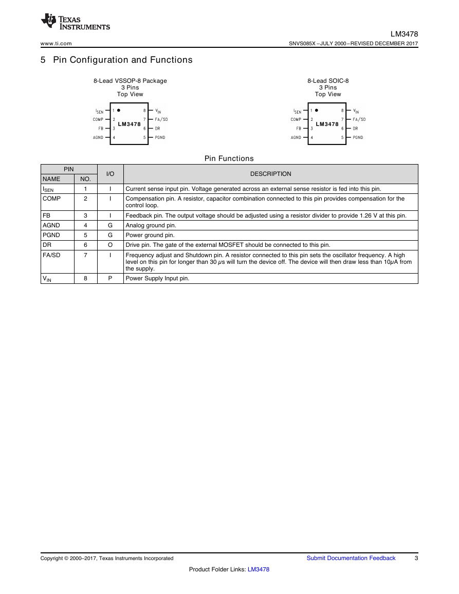
5 Pin Configuration and Functions
LM3478
SNVS085X –JULY 2000–REVISED DECEMBER 2017
8-Lead VSSOP-8 Package
3 Pins
Top View
8-Lead SOIC-8
3 Pins
Top View
PIN
NAME
ISEN
COMP
FB
AGND
PGND
DR
FA/SD
VIN
NO.
1
2
3
4
5
6
7
8
I/O
I
I
I
G
G
O
I
P
Pin Functions
DESCRIPTION
Current sense input pin. Voltage generated across an external sense resistor is fed into this pin.
Compensation pin. A resistor, capacitor combination connected to this pin provides compensation for the
control loop.
Feedback pin. The output voltage should be adjusted using a resistor divider to provide 1.26 V at this pin.
Analog ground pin.
Power ground pin.
Drive pin. The gate of the external MOSFET should be connected to this pin.
Frequency adjust and Shutdown pin. A resistor connected to this pin sets the oscillator frequency. A high
level on this pin for longer than 30 µs will turn the device off. The device will then draw less than 10µA from
the supply.
Power Supply Input pin.
Copyright © 2000–2017, Texas Instruments Incorporated
Submit Documentation Feedback
3
Product Folder Links: LM3478
�
www.ti.com
MIN
–0.4< V
–0.4 < VFA/SD
MAX
45
V FB < 7
VFA/SD< 7
1
UNIT
V
V
V
A
Internally Limited
+150
215
260
–0.4 ≤ VDR
VDR ≤ 8
°C
°C
°C
V
mV
°C
LM3478
SNVS085X –JULY 2000–REVISED DECEMBER 2017
6 Specifications
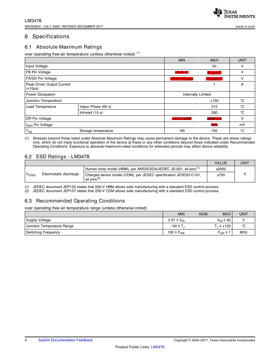
6.1 Absolute Maximum Ratings
over operating free-air temperature (unless otherwise noted) (1)
Input Voltage
FB Pin Voltage
FA/SD Pin Voltage
Peak Driver Output Current
(<10µs)
Power Dissipation
Junction Temperature
Lead Temperature
Vapor Phase (60 s)
Infrared (15 s)
DR Pin Voltage
ISEN Pin Voltage
Tstg
(1) Stresses beyond those listed under Absolute Maximum Ratings may cause permanent damage to the device. These are stress ratings
Storage temperature
500
150
−65
only, which do not imply functional operation of the device at these or any other conditions beyond those indicated under Recommended
Operating Conditions. Exposure to absolute-maximum-rated conditions for extended periods may affect device reliability.
6.2 ESD Ratings - LM3478
V(ESD)
Electrostatic discharge
Human body model (HBM), per ANSI/ESDA/JEDEC JS-001, all pins(1)
Charged device model (CDM), per JEDEC specification JESD22-C101,
all pins(2)
VALUE
±2000
±750
UNIT
V
(1)
(2)
JEDEC document JEP155 states that 500-V HBM allows safe manufacturing with a standard ESD control process.
JEDEC document JEP157 states that 250-V CDM allows safe manufacturing with a standard ESD control process.
6.3 Recommended Operating Conditions
over operating free-air temperature range (unless otherwise noted)
Supply Voltage
Junction Temperature Range
Switching Frequency
MIN
2.97 ≤ VIN
−40 ≤ TJ
100 ≤ FSW
NOM
MAX
VIN ≤ 40
TJ ≤ +125
FSW ≤ 1
UNIT
V
°C
MHz
4
Submit Documentation Feedback
Copyright © 2000–2017, Texas Instruments Incorporated
Product Folder Links: LM3478
�
www.ti.com
6.4 Thermal Information
LM3478
SNVS085X –JULY 2000–REVISED DECEMBER 2017
THERMAL METRIC(1)
LM3478
D
UNIT
Junction-to-ambient thermal resistance
Junction-to-case (top) thermal resistance
Junction-to-board thermal resistance
Junction-to-top characterization parameter
Junction-to-board characterization parameter
Junction-to-case (bottom) thermal resistance
RθJA
RθJC(top)
RθJB
ψJT
ψJB
RθJC(bot)
(1) For more information about traditional and new thermal metrics, see the IC Package Thermal Metrics application report, SPRA953.
°C/W
°C/W
°C/W
°C/W
°C/W
°C/W
8 PINS
105.3
50.3
55.8
6.8
54.7
N/A
DGK
8 PINS
157.2
49.9
77.1
4.7
75.8
N/A
PARAMETER
6.5 Electrical Characteristics
Unless otherwise specified, VIN = 12V, RFA = 40kΩ, TJ = 25°C
TEST CONDITIONS
VCOMP = 1.4V, 2.97 ≤ VIN ≤ 40V
VCOMP = 1.4V, 2.97 ≤ VIN ≤ 40V, −40°C
≤ TJ ≤ 125°C
2.97 ≤ VIN ≤ 40V
Feedback Voltage
VFB
ΔVLINE
Feedback Voltage Line
Regulation
Output Voltage Load
Regulation
Input Undervoltage
Lock-out
Input Undervoltage
Lock-out Hysteresis
Nominal Switching
Frequency
Driver Switch On
Resistance (top)
Driver Switch On
Resistance (bottom)
Maximum Drive Voltage
Swing(1)
Maximum Duty Cycle(2)
ΔVLOAD
VUVLO
VUV(HYS)
Fnom
RDS1 (ON)
RDS2 (ON)
VDR (max)
Dmax
IEAO Source/Sink
−40°C ≤ TJ ≤ 125°C
−40°C ≤ TJ ≤ 125°C
RFA = 40KΩ
RFA = 40KΩ, −40°C ≤ TJ ≤ 125°C
IDR = 0.2A, VIN= 5V
IDR = 0.2A
VIN < 7.2V
VIN ≥ 7.2V
Tmin (on)
Minimum On Time
ISUPPLY
Supply Current (non-
switching)
IQ
VSENSE
VSC
Quiescent Current in
Shutdown Mode
Current Sense
Threshold Voltage
Short-Circuit Current
Limit Sense Voltage
−40°C ≤ TJ ≤ 125°C
See (3)
See (3), −40°C ≤ TJ ≤ 125°C
VFA/SD = 5V (4), VIN = 5V
VFA/SD = 5V (4), VIN = 5V, −40°C ≤ TJ ≤
125°C
VIN = 5V
VIN = 5V, −40°C ≤ TJ ≤ 125°C
VIN = 5V
VIN = 5V, −40°C ≤ TJ ≤ 125°C
MIN
1.2416
1.228
130
350
210
135
125
250
TYP
1.26
0.001
2.85
170
400
16
4.5
VIN
7.2
100%
325
2.7
5
156
343
MAX
1.2843
1.292
±0.5
2.97
210
440
600
3.3
10
180
190
415
UNIT
V
%/V
%/A
V
mV
kHz
Ω
V
ns
mA
µA
mV
mV
(1) The voltage on the drive pin, VDR is equal to the input voltage when input voltage is less than 7.2 V. VDR is equal to 7.2 V when the
input voltage is greater than or equal to 7.2 V.
(2) The limits for the maximum duty cycle can not be specified since the part does not permit less than 100% maximum duty cycle
operation.
(3) For this test, the FA/SD pin is pulled to ground using a 40-K resistor.
(4) For this test, the FA/SD pin is pulled to 5 V using a 40-K resistor.
Copyright © 2000–2017, Texas Instruments Incorporated
Submit Documentation Feedback
5
Product Folder Links: LM3478
�
LM3478
SNVS085X –JULY 2000–REVISED DECEMBER 2017
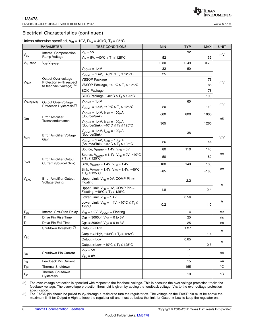
Electrical Characteristics (continued)
Unless otherwise specified, VIN = 12V, RFA = 40kΩ, TJ = 25°C
TEST CONDITIONS
PARAMETER
Internal Compensation
Ramp Voltage
VSL/VSENSE
VSL
VSL ratio
VOVP
Output Over-voltage
Protection (with respect
to feedback voltage) (5)
VOVP(HYS) Output Over-Voltage
Protection Hysteresis(5)
Gm
AVOL
IEAO
VEAO
TSS
Tr
Tf
VSD
ISD
IFB
TSD
Tsh
VIN = 5V
VIN = 5V, −40°C ≤ TJ ≤ 125°C
VCOMP = 1.4V
VCOMP = 1.4V, −40°C ≤ TJ ≤ 125°C
VSSOP Package
VSSOP Package, −40°C ≤ TJ ≤ 125°C
SOIC Package
SOIC Package, −40°C ≤ TJ ≤ 125°C
VCOMP = 1.4V
VCOMP = 1.4V, −40°C ≤ TJ ≤ 125°C
VCOMP = 1.4V, IEAO = 100µA
(Source/Sink)
VCOMP = 1.4V, IEAO = 100µA
(Source/Sink), −40°C ≤ TJ ≤ 125°C
VCOMP = 1.4V, IEAO = 100µA
(Source/Sink)
VCOMP = 1.4V, IEAO = 100µA
(Source/Sink), −40°C ≤ TJ ≤ 125°C
Source, VCOMP = 1.4V, VFB = 0V
Source, VCOMP = 1.4V, VFB = 0V, −40°C
≤ TJ ≤ 125°C
Sink, VCOMP = 1.4V, VFB = 1.4V
Sink, VCOMP = 1.4V, VFB = 1.4V, −40°C
≤ TJ ≤ 125°C
Upper Limit, VFB = 0V, COMP Pin =
Floating
Upper Limit, VFB = 0V, COMP Pin =
Floating, −40°C ≤ TJ ≤ 125°C
Lower Limit, VFB = 1.4V
Lower Limit, VFB = 1.4V, −40°C ≤ TJ ≤
125°C
Error Amplifier
Transconductance
Error Amplifier Voltage
Gain
Error Amplifier Output
Current (Source/ Sink)
Error Amplifier Output
Voltage Swing
Internal Soft-Start Delay VFB = 1.2V, VCOMP = Floating
Drive Pin Rise Time
Cgs = 3000pf, VDR = 0 to 3V
Cgs = 3000pf, VDR = 0 to 3V
Drive Pin Fall Time
Shutdown threshold (6)
Output = High
Output = High, −40°C ≤ TJ ≤ 125°C
Output = Low
Output = Low, −40°C ≤ TJ ≤ 125°C
VSD = 5V
VSD = 0V
Shutdown Pin Current
Feedback Pin Current
Thermal Shutdown
Thermal Shutdown
Hysteresis
MIN
52
0.30
32
25
20
600
365
26
80
50
−100
−85
1.8
0.2
www.ti.com
MAX
UNIT
132
0.70
78
85
78
100
110
1000
1265
44
140
180
−180
−185
2.4
1.0
1.4
0.3
mV
mV
mV
µS
V/V
µA
µA
V
V
ms
ns
ns
V
V
µA
nA
°C
°C
TYP
92
0.49
50
60
800
38
110
−140
2.2
0.56
4
25
25
1.27
0.65
−1
+1
15
165
10
(5) The over-voltage protection is specified with respect to the feedback voltage. This is because the over-voltage protection tracks the
feedback voltage. The overvoltage protection threshold is given by adding the feedback voltage, VFB to the over-voltage protection
specification.
(6) The FA/SD pin should be pulled to VIN through a resistor to turn the regulator off. The voltage on the FA/SD pin must be above the
maximum limit for Output = High to keep the regulator off and must be below the limit for Output = Low to keep the regulator on.
6
Submit Documentation Feedback
Copyright © 2000–2017, Texas Instruments Incorporated
Product Folder Links: LM3478
�
www.ti.com
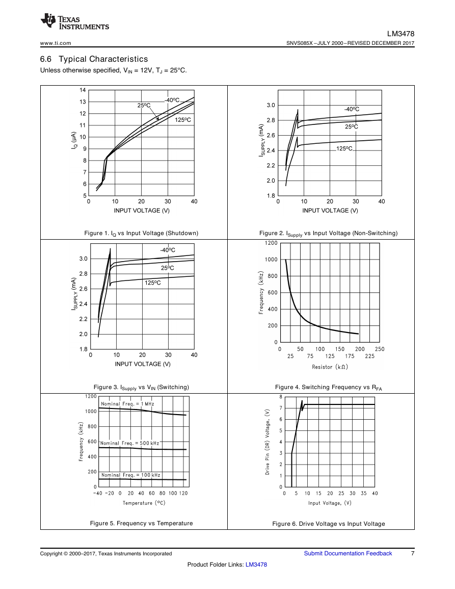
6.6 Typical Characteristics
Unless otherwise specified, VIN = 12V, TJ = 25°C.
LM3478
SNVS085X –JULY 2000–REVISED DECEMBER 2017
Figure 1. IQ vs Input Voltage (Shutdown)
Figure 2. ISupply vs Input Voltage (Non-Switching)
Figure 3. ISupply vs VIN (Switching)
Figure 4. Switching Frequency vs RFA
Figure 5. Frequency vs Temperature
Figure 6. Drive Voltage vs Input Voltage
Copyright © 2000–2017, Texas Instruments Incorporated
Submit Documentation Feedback
7
Product Folder Links: LM3478
�
LM3478
SNVS085X –JULY 2000–REVISED DECEMBER 2017
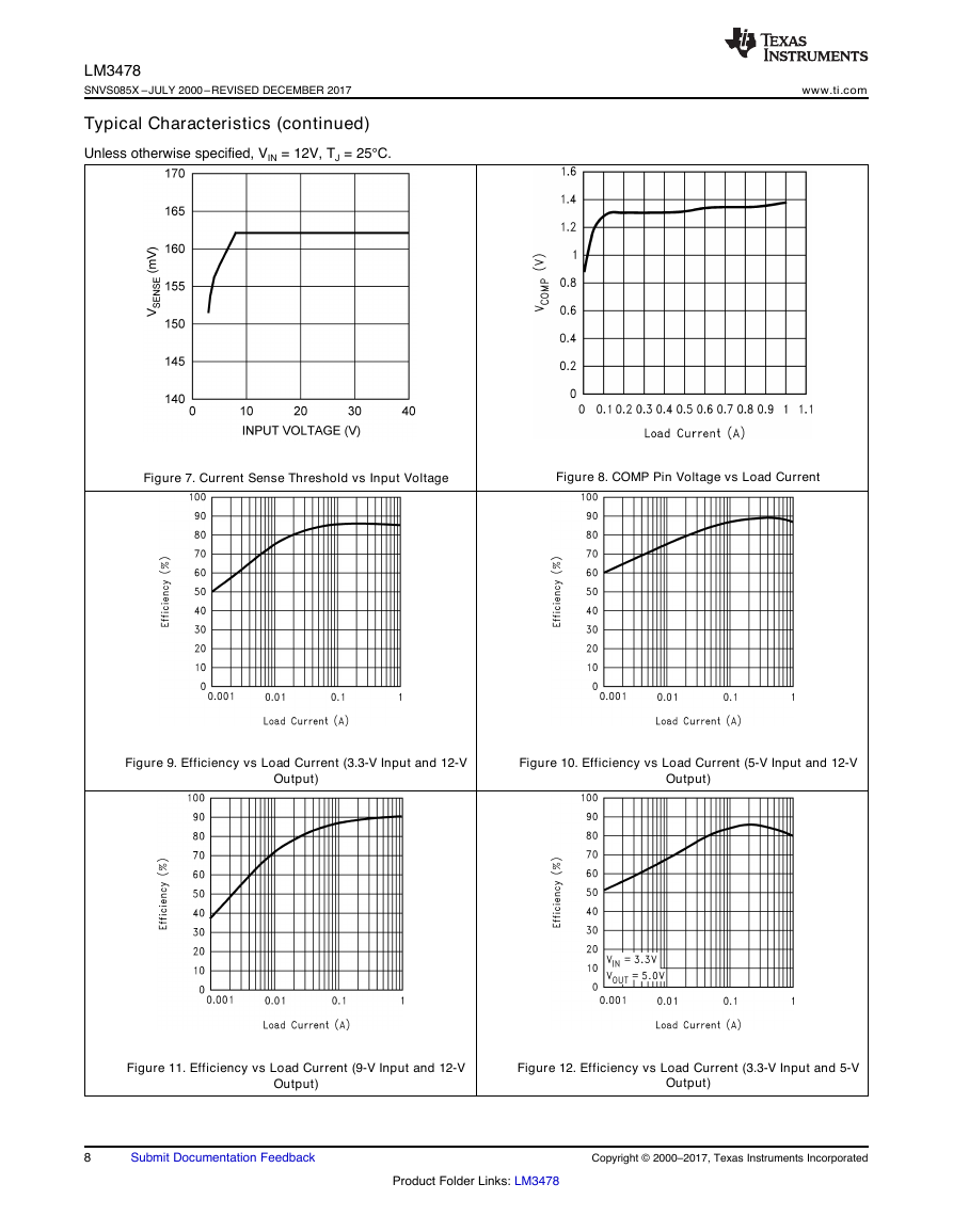
Typical Characteristics (continued)
Unless otherwise specified, VIN = 12V, TJ = 25°C.
www.ti.com
Figure 7. Current Sense Threshold vs Input Voltage
Figure 8. COMP Pin Voltage vs Load Current
Figure 9. Efficiency vs Load Current (3.3-V Input and 12-V
Output)
Figure 10. Efficiency vs Load Current (5-V Input and 12-V
Output)
Figure 11. Efficiency vs Load Current (9-V Input and 12-V
Output)
Figure 12. Efficiency vs Load Current (3.3-V Input and 5-V
Output)
8
Submit Documentation Feedback
Copyright © 2000–2017, Texas Instruments Incorporated
Product Folder Links: LM3478
�



 2023年江西萍乡中考道德与法治真题及答案.doc
 2012年重庆南川中考生物真题及答案.doc
 2013年江西师范大学地理学综合及文艺理论基础考研真题.doc
 2020年四川甘孜小升初语文真题及答案I卷.doc
 2020年注册岩土工程师专业基础考试真题及答案.doc
 2023-2024学年福建省厦门市九年级上学期数学月考试题及答案.doc
 2021-2022学年辽宁省沈阳市大东区九年级上学期语文期末试题及答案.doc
 2022-2023学年北京东城区初三第一学期物理期末试卷及答案.doc
 2018上半年江西教师资格初中地理学科知识与教学能力真题及答案.doc
 2012年河北国家公务员申论考试真题及答案-省级.doc
 2020-2021学年江苏省扬州市江都区邵樊片九年级上学期数学第一次质量检测试题及答案.doc
 2022下半年黑龙江教师资格证中学综合素质真题及答案.doc