Evaluation Board User Guide
UG-207
One Technology Way • P.O. Box 9106 • Norwood, MA 02062-9106, U.S.A. • Tel: 781.329.4700 • Fax: 781.461.3113 • www.analog.com
Evaluation Board for 1 GSPS DDS with 14-Bit DAC
FEATURES
Full-featured evaluation board for the AD9910
PC evaluation software for control and measurement of the
AD9910
USB interface
Graphic user interface (GUI) software with frequency sweep
capability for board control and data analysis
Factory tested and ready to use
PACKAGE CONTENTS
AD9910 evaluation board
AD9910/PCBZ installation software CD
USB cable
GENERAL DESCRIPTION
This user guide describes how to set up and use the AD9910
evaluation board. The AD9910 is a 1 GSPS DDS with a
14-bit DAC.
The evaluation board software provides a graphical user interface
(GUI) for easy communication with the device along with many
user-friendly features such as the mouse-over effect.
This user guide is intended for use in conjunction with the
AD9910 data sheet, which is available from Analog Devices,
Inc., at www.analog.com.
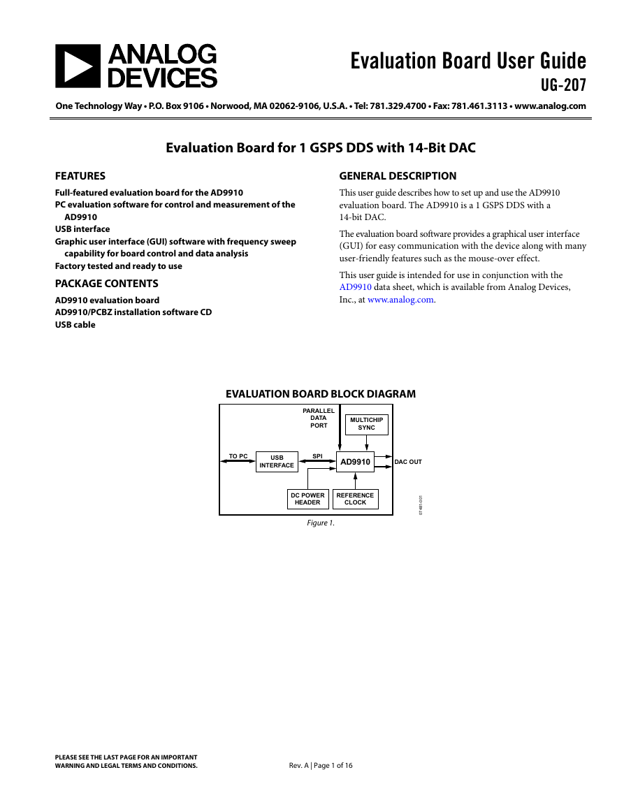
EVALUATION BOARD BLOCK DIAGRAM
PARALLEL
DATA
PORT
MULTICHIP
SYNC
TO PC
USB
INTERFACE
SPI
AD9910
DAC OUT
DC POWER
HEADER
REFERENCE
CLOCK
Figure 1.
1
0
0
-
1
8
4
7
0
PLEASE SEE THE LAST PAGE FOR AN IMPORTANT
WARNING AND LEGAL TERMS AND CONDITIONS.
Rev. A | Page 1 of 16
�
Evaluation Board User Guide
Installing the Software..................................................................5
Installing the Driver......................................................................5
Launching the Program................................................................5
Control Window............................................................................7
Profiles Window............................................................................9
Single-Tone Mode .........................................................................9
View Windows............................................................................ 11
OSK and Digital Ramp Control ............................................... 12
Multichip Sync Control ............................................................. 13
RAM Operation.......................................................................... 14
Debug........................................................................................... 15
Register Map (Software Buffer) Values ................................... 15
UG-207
TABLE OF CONTENTS
Features .............................................................................................. 1
Package Contents.............................................................................. 1
General Description......................................................................... 1
Evaluation Board Block Diagram................................................... 1
Revision History ............................................................................... 2
Evaluation Board Hardware............................................................ 3
Requirements ................................................................................ 3
Setting Up the Evaluation Board................................................ 3
Connectors .................................................................................... 3
Jumpers .......................................................................................... 3
Evaluation Board Layout ............................................................. 4
Evaluation Board Software.............................................................. 5
REVISION HISTORY
10/10—Rev. 0 to Rev. A
Document Title Changed from AD9910/PCBZ to
UG-207.................................................................................Universal
Updated Format..................................................................Universal
Changes to Device Clock Oscillator Options Section ................. 3
Changes to Power Down Digital, DAC, Clock Input, and Aux
DAC Section...................................................................................... 8
Change to DUT I/O Section ......................................................... 16
Deleted Ordering Information Section ....................................... 17
4/08—Revision 0: Initial Version
Rev. A | Page 2 of 16
�
Evaluation Board User Guide
EVALUATION BOARD HARDWARE
REQUIREMENTS
To successfully use the evaluation board and run the software,
the requirements listed in Table 1 must be met.
Requirement
Windows® 98/ME/2000/XP
Table 1. AD9910/PCBZ Requirements
Item
Operating
System
Processor
Memory
Ports
Clocking
Pentium® I or later
128 MB minimum
One USB port
Signal generator capable of generating
sinusoidal waves of at least 0 dBm, up to at
least 10 MHz
Power Supplies Capability to generate at least two
Measurement
Cables
independent dc voltages (1.8 V/3.3 V)
Appropriate measurement device, such as a
spectrum analyzer or a high bandwidth
oscilloscope
USB 1.1/2.0 cable, and SMA-to-X cables (X =
SMA or BNC, depending on the connector of
the device interfacing with the board)
SETTING UP THE EVALUATION BOARD
DC Power Supply
The AD9910 evaluation board has two power supply connectors
(four pins each): TB1 and TB2. TB1 powers the USB interface
circuitry, the digital I/O interface, and the digital core. TB2
powers the DAC and the clock input circuitry.
CONNECTORS
Table 2 shows the necessary connections and the appropriate
biasing voltage.
Table 2. Connections and Biasing Voltage
Connector
TB1
TB1
TB1
TB1
TB2
TB2
TB2
Label
VCC_USB
GND
DVDD_IO
DVDD
GND
DAC_VDD
CLK_VDD
Pin No.
1
2
3
4
1, 3
2
4
Voltage (V)
3.3
0
3.3
1.8
0
3.3
1.8
UG-207
Device Clock Oscillator Options
The AD9910 architecture provides the user with three options
when providing an input signal to the part. The first option allows
the user to provide a high frequency input signal, connected to J1.
The second option allows the user to connect using a lower input
reference frequency, enabling the clock multiplier, and connects
through J1. The third option allows the user to connect a crystal
resonator on the backside of the board.
Note that the AD9910 evaluation board does not populate the
PLL loop filter components. Therefore, to use the internal PLL of
the AD9910, the user must solder down these components, or
else the PLL is not stable. The AD9910 data sheet has helpful
formulas to calculate the appropriate values. In addition, an Excel
file to help choose the loop filter component values is available at
www.analog.com. Go to the AD9910 product page and click on
the Evaluation Boards and Development Kits tab.
To enable the crystal mode, switch the jumper, W7, to the XTAL
mode. Remove C51 and 52. Place 0 (zero) Ω resistors at R4 and
R11 on the backside of the board. The crystal oscillates at 25 MHz.
Refer to the AD9910 data sheet for details on the maximum input
speeds and input sensitivities of these two inputs.
Device Communication Requirements
Two interface options are available on the evaluation board.
• USB 1.1/2.0
• Header row (U5 and U9), which places the part under the
control of an external controller (such as a microprocessor,
FPGA, or DSP)
Analog Devices provides a GUI for the PC; it does not provide
control software for external controllers.
JUMPERS
Use the jumper settings listed in Table 3 to enable different
modes of communication.
Table 3. Jumper Settings for Communication Modes
Mode
PC Control,
USB Port
Settings
Set Jumper W1 and Jumper W2 to enable. Set
Jumper W4 to enable. Place a jumper on W5, W6,
and W3.
Set Jumper W1and Jumper W2 to disable. Set
Jumper W4 to disable. Remove the jumper on
W5, W6, and W3.
External
Control
Jumper W1, Jumper W2, and Jumper W4 enable the USB
circuitry to control the AD9910. Jumper W3 controls the
EEPROM, used in starting up the USB circuitry. Jumper W5
and Jumper W6 control Signal SDO and Signal SDIO to and
from the AD9910.
Rev. A | Page 3 of 16
�
UG-207
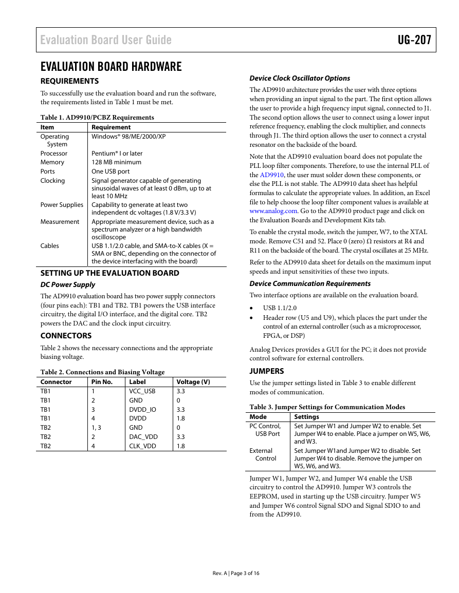
EVALUATION BOARD LAYOUT
Evaluation Board User Guide
STATUS PINS
MANUAL I/O
CONTROL HEADERS
MULTIDEVICE
SYCNHRONOUS CONTROL
CLOCK MODE
SELECT
REF
CLOCK
INPUT
DAC
OUTPUT
2
0
0
-
1
8
4
7
0
USB PORT
POWER SUPPLY
CONNECTIONS
Figure 2. AD9910 PCB Evaluation Board
Manual I/O Control Headers
These pins provide the communication interface for the
AD9910 when the part is under the command of an external
controller (see Table 3 for correct jumper settings).
Multidevice Synchronous Control
These connections set up the AD9910 for multidevice
synchronous operation.
DAC Output
These connections represent the filtered or unfiltered (default)
output of the DAC.
Clock Mode Select
This connection controls whether the reference clock source is a
20 MHz to 30 MHz crystal, or is from an external signal generator.
A 25 MHz crystal is provided on the underside of the AD9910
evaluation board.
Ref Clock Input
This is the input for the external reference clock signal.
Power Supply Connections
These two connectors, TB1 and TB2, provide all necessary
supply voltages needed by the AD9910 and the evaluation board
(see Table 2).
USB Port
When the part is under PC control (default mode), the evaluation
board communicates with the AD9910 via this port.
Rev. A | Page 4 of 16
�
Evaluation Board User Guide
EVALUATION BOARD SOFTWARE
INSTALLING THE SOFTWARE
Follow these steps to install the AD9910 evaluation software:
1. Log into your PC system with administrative privileges.
2. Uninstall any previous versions of the AD9910 evaluation
3.
software from your PC system.
Insert the AD9910 evaluation software CD into your
CD-ROM drive. Do not connect the AD9910 evaluation
board to the computer until the AD9910 evaluation
software has been successfully installed. Refer to the
Readme.txt file located in the Software folder before
proceeding with the installation of the AD9910 evaluation
software.
4. Run the setup.exe file located in the Software folder and
follow the AD9910 evaluation software onscreen
installation instructions.
INSTALLING THE DRIVER
Once the software is successfully installed onto your PC, the
next step is to interface the AD9910 evaluation software to the
AD9910 evaluation board via the USB Port (see Figure 2).
In order for the evaluation board and software to communicate
properly, drivers must be loaded onto your PC system. The
following instructions explain how to install these drivers on
your PC system.
Windows 98/ME/2000 Users
1. Power up the AD9910 evaluation board (see Table 2).
2. Connect the evaluation board to the computer using a USB
cable via the USB port. Then, the VBUS LED (CR1 on the
AD9910 evaluation board) illuminates. When the USB
cable is connected, the Found New Hardware Wizard
window appears.
If you are using Windows 2000, click Finish in the Found
New Hardware Wizard.
3.
After the window has disappeared, the USB Status LED (CR2
on the AD9910 evaluation board) flashes, which indicates that
the evaluation board is connected properly.
UG-207
Windows XP Users
1. Power up the AD9910 evaluation board (see Table 2).
2. Connect the evaluation board to the computer via the USB
port using a USB cable. Then, the VBUS LED (CR1 on the
AD9910 evaluation board) illuminates.
3. When the USB cable is connected, the Found New
Hardware Wizard appears. Click Next to continue to the
AD9910 Firmware Loader.
4. Click Continue Anyway when the Hardware Installation
Warning window appears.
5. Click Finish in the Found New Hardware Wizard when
installation is complete.
6. Click Next when the next Found New Hardware Wizard
appears. This is for the EZSSP device.
7. Click Continue Anyway when the Hardware Installation
Warning window appears.
8. Click Finish in the Found New Hardware Wizard when
installation is complete.
Once the Found New Hardware Wizard window disappears,
the USB status LED (CR2 on the AD9910 evaluation board)
flashes, which indicates that the evaluation board is connected
properly. If the LED does not flash, verify that all power and USB
connections are properly connected.
LAUNCHING THE PROGRAM
Follow these three steps to load the AD9910 evaluation
software:
1. Before starting the software, make sure that the AD9910
evaluation board is powered up, connected to the computer,
and that the USB status LED is flashing.
2. Click the Start button, located at the bottom left-hand
corner of your screen.
3. Select Programs, then the AD9910 Eval Software folder,
and then AD9910 Eval Software to load the software.
One of several status messages appears. These messages are
discussed in further detail in the next section, Status Messages
Upon Loading Software.
Rev. A | Page 5 of 16
�
UG-207
Status Messages Upon Loading Software
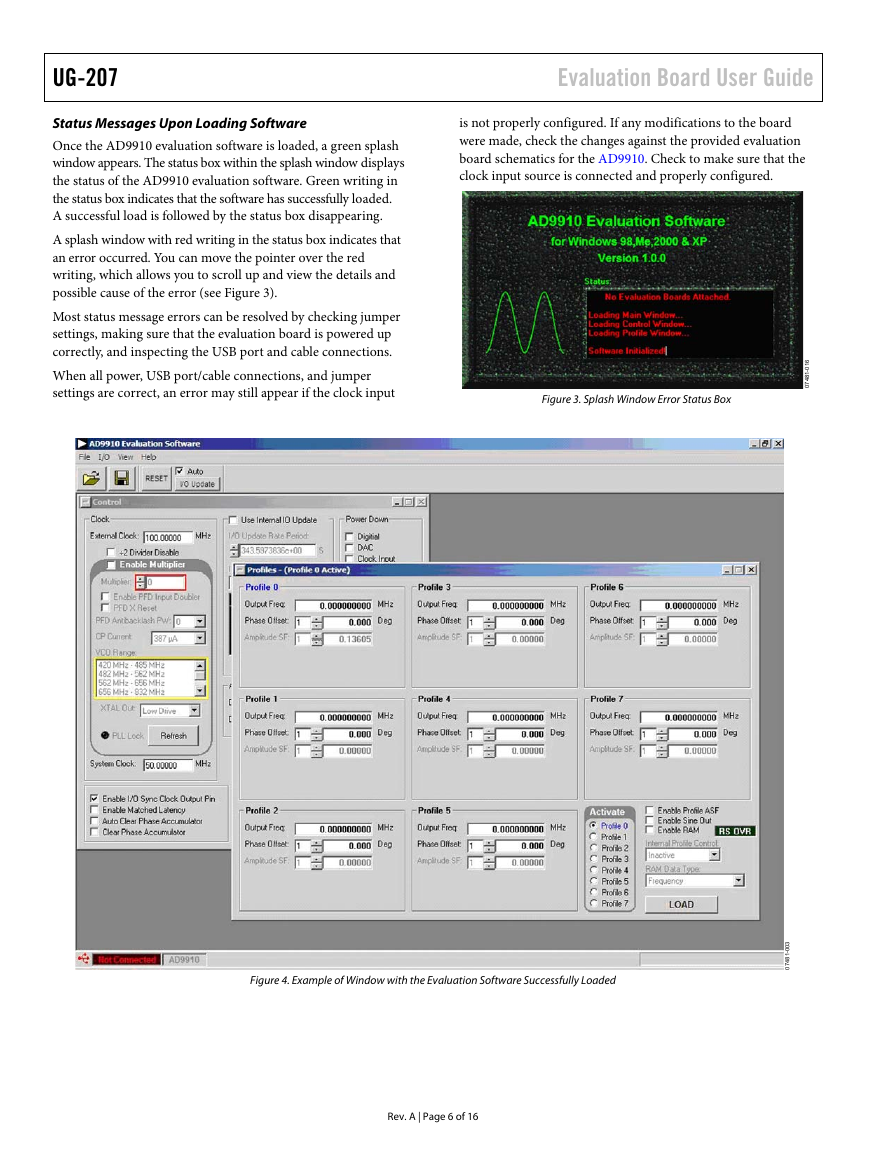
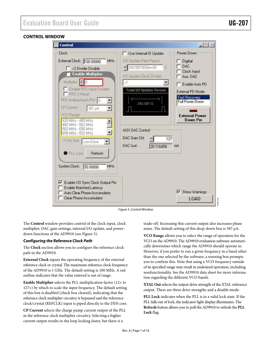
Once the AD9910 evaluation software is loaded, a green splash
window appears. The status box within the splash window displays
the status of the AD9910 evaluation software. Green writing in
the status box indicates that the software has successfully loaded.
A successful load is followed by the status box disappearing.
A splash window with red writing in the status box indicates that
an error occurred. You can move the pointer over the red
writing, which allows you to scroll up and view the details and
possible cause of the error (see Figure 3).
Most status message errors can be resolved by checking jumper
settings, making sure that the evaluation board is powered up
correctly, and inspecting the USB port and cable connections.
When all power, USB port/cable connections, and jumper
settings are correct, an error may still appear if the clock input
Evaluation Board User Guide
is not properly configured. If any modifications to the board
were made, check the changes against the provided evaluation
board schematics for the AD9910. Check to make sure that the
clock input source is connected and properly configured.
Figure 3. Splash Window Error Status Box
6
1
0
-
1
8
4
7
0
Figure 4. Example of Window with the Evaluation Software Successfully Loaded
3
0
0
-
1
8
4
7
0
Rev. A | Page 6 of 16
�
Evaluation Board User Guide
CONTROL WINDOW
UG-207
Figure 5. Control Window
4
0
0
-
1
8
4
7
0
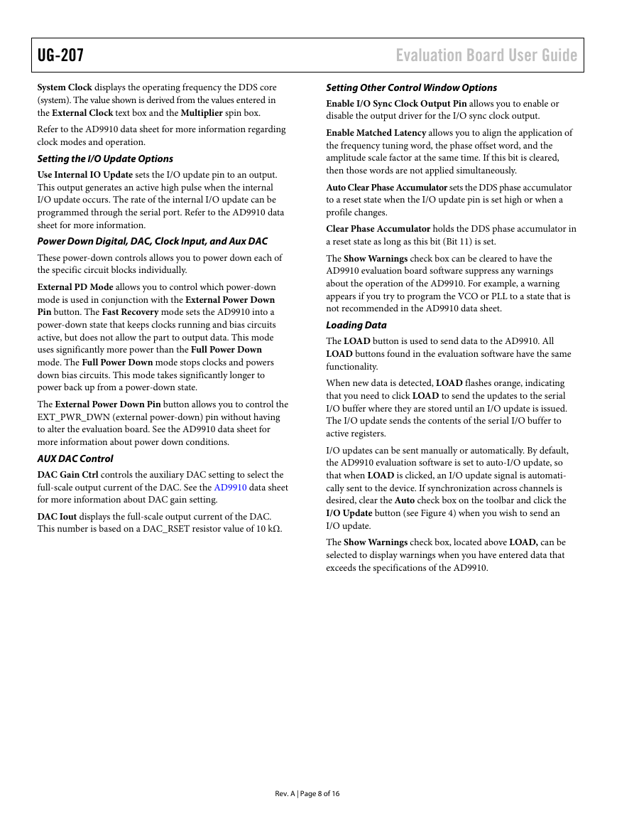
The Control window provides control of the clock input, clock
multiplier, DAC gain settings, internal I/O update, and power-
down functions of the AD9910 (see Figure 5).
Configuring the Reference Clock Path
The Clock section allows you to configure the reference clock
path in the AD9910.
External Clock inputs the operating frequency of the external
reference clock or crystal. The maximum reference clock frequency
of the AD9910 is 1 GHz. The default setting is 100 MHz. A red
outline indicates that the value entered is out of range.
Enable Multiplier selects the PLL multiplication factor (12× to
127×) by which to scale the input frequency. The default setting
of this box is disabled (check box cleared), indicating that the
reference clock multiplier circuitry is bypassed and the reference
clock/crystal (REFCLK) input is piped directly to the DDS core.
CP Current selects the charge pump current output of the PLL
in the reference clock multiplier circuitry. Selecting a higher
current output results in the loop locking faster, but there is a
trade-off. Increasing this current output also increases phase
noise. The default setting of this drop-down box is 387 μA.
VCO Range allows you to select the range of operation for the
VCO on the AD9910. The AD9910 evaluation software automati-
cally determines which range the AD9910 should operate in.
However, if you prefer to run a given frequency in a band other
than the one selected by the software, a warning box prompts
you to confirm this. Note that using a VCO frequency outside
of its specified range may result in undesired operation, including
nonfunctionality. See the AD9910 data sheet for more informa-
tion regarding the different VCO bands.
XTAL Out selects the output drive strength of the XTAL reference
output. There are three drive strengths and a disable mode.
PLL Lock indicates when the PLL is in a valid lock state. If the
PLL falls out of lock, the indicator light display illuminates. The
Refresh button allows you to poll the AD9910 to refresh the PLL
Lock flag.
Rev. A | Page 7 of 16
�
UG-207
System Clock displays the operating frequency the DDS core
(system). The value shown is derived from the values entered in
the External Clock text box and the Multiplier spin box.
Refer to the AD9910 data sheet for more information regarding
clock modes and operation.
Setting the I/O Update Options
Use Internal IO Update sets the I/O update pin to an output.
This output generates an active high pulse when the internal
I/O update occurs. The rate of the internal I/O update can be
programmed through the serial port. Refer to the AD9910 data
sheet for more information.
Power Down Digital, DAC, Clock Input, and Aux DAC
These power-down controls allows you to power down each of
the specific circuit blocks individually.
External PD Mode allows you to control which power-down
mode is used in conjunction with the External Power Down
Pin button. The Fast Recovery mode sets the AD9910 into a
power-down state that keeps clocks running and bias circuits
active, but does not allow the part to output data. This mode
uses significantly more power than the Full Power Down
mode. The Full Power Down mode stops clocks and powers
down bias circuits. This mode takes significantly longer to
power back up from a power-down state.
The External Power Down Pin button allows you to control the
EXT_PWR_DWN (external power-down) pin without having
to alter the evaluation board. See the AD9910 data sheet for
more information about power down conditions.
AUX DAC Control
DAC Gain Ctrl controls the auxiliary DAC setting to select the
full-scale output current of the DAC. See the AD9910 data sheet
for more information about DAC gain setting.
DAC Iout displays the full-scale output current of the DAC.
This number is based on a DAC_RSET resistor value of 10 kΩ.
Evaluation Board User Guide
Setting Other Control Window Options
Enable I/O Sync Clock Output Pin allows you to enable or
disable the output driver for the I/O sync clock output.
Enable Matched Latency allows you to align the application of
the frequency tuning word, the phase offset word, and the
amplitude scale factor at the same time. If this bit is cleared,
then those words are not applied simultaneously.
Auto Clear Phase Accumulator sets the DDS phase accumulator
to a reset state when the I/O update pin is set high or when a
profile changes.
Clear Phase Accumulator holds the DDS phase accumulator in
a reset state as long as this bit (Bit 11) is set.
The Show Warnings check box can be cleared to have the
AD9910 evaluation board software suppress any warnings
about the operation of the AD9910. For example, a warning
appears if you try to program the VCO or PLL to a state that is
not recommended in the AD9910 data sheet.
Loading Data
The LOAD button is used to send data to the AD9910. All
LOAD buttons found in the evaluation software have the same
functionality.
When new data is detected, LOAD flashes orange, indicating
that you need to click LOAD to send the updates to the serial
I/O buffer where they are stored until an I/O update is issued.
The I/O update sends the contents of the serial I/O buffer to
active registers.
I/O updates can be sent manually or automatically. By default,
the AD9910 evaluation software is set to auto-I/O update, so
that when LOAD is clicked, an I/O update signal is automati-
cally sent to the device. If synchronization across channels is
desired, clear the Auto check box on the toolbar and click the
I/O Update button (see Figure 4) when you wish to send an
I/O update.
The Show Warnings check box, located above LOAD, can be
selected to display warnings when you have entered data that
exceeds the specifications of the AD9910.
Rev. A | Page 8 of 16
�



 2023年江西萍乡中考道德与法治真题及答案.doc
 2012年重庆南川中考生物真题及答案.doc
 2013年江西师范大学地理学综合及文艺理论基础考研真题.doc
 2020年四川甘孜小升初语文真题及答案I卷.doc
 2020年注册岩土工程师专业基础考试真题及答案.doc
 2023-2024学年福建省厦门市九年级上学期数学月考试题及答案.doc
 2021-2022学年辽宁省沈阳市大东区九年级上学期语文期末试题及答案.doc
 2022-2023学年北京东城区初三第一学期物理期末试卷及答案.doc
 2018上半年江西教师资格初中地理学科知识与教学能力真题及答案.doc
 2012年河北国家公务员申论考试真题及答案-省级.doc
 2020-2021学年江苏省扬州市江都区邵樊片九年级上学期数学第一次质量检测试题及答案.doc
 2022下半年黑龙江教师资格证中学综合素质真题及答案.doc