Data Sheet - Confidential
DOC 56-34-01508 • Rev 1.0 • March 2017
iNAND® 7250
e.MMC 5.1 with HS400 Interface
Confidential, subject to all applicable non-disclosure agreements
www.SanDisk.com
�
Confidential
SanDisk® iNAND 7250 e.MMC 5.1+ HS400 I/F data sheet
REVISION HISTORY
Doc. No
Revision
Date
Description
DOC-56-34-01508
1.0
March - 2016
Released version
SanDisk® provides this information, and any related samples, products, and documentation (collectively the “Materials”) solely
for the selection and use of SanDisk® products. To the maximum extent permitted by applicable law: (1) Materials are made
available “AS IS” and with all faults, SanDisk hereby DISCLAIMS ALL WARRANTIES AND CONDITIONS, EXPRESS, IMPLIED,
STATUTORY, OR OTHERWISE, INCLUDING BUT NOT LIMITED TO WARRANTIES OF MERCHANTABILITY, NON-INFRINGEMENT, OR
FITNESS FOR ANY PARTICULAR PURPOSE; and (2) SanDisk shall not be liable (whether in contract or tort, including negligence,
or under any other theory of liability) for any loss or damage of any kind or nature related to, arising under, or in connection
with, the Materials (including your use of the Materials), including for any direct, indirect, special, incidental, or consequential
loss or damage (including loss of data, profits, goodwill, or any type of loss or damage suffered as a result of any action brought
by a third party) even if such damage or loss was reasonably foreseeable or SanDisk® had been advised of the possibility of the
same. You are responsible for obtaining any rights required in connection with your use of the Materials. The Materials are
subject to change without further notice. SanDisk®assumes no obligation to correct errors or to notify you of updates to the
Materials or to product specifications. You may not reverse engineer, reproduce, modify, distribute, or publicly display the
Materials without prior written consent of SanDisk. SanDisk products are not designed or intended to be fail-safe or for use in
any application requiring fail-safe performance. You assume sole risk and liability for use of SanDisk products in critical
applications.
© 2017 Western Digital Corporation or its affiliates. All rights reserved. Specifications are subject to change. SanDisk® is a
trademark of Western Digital Corporation or its affiliates, registered in the United States and other countries. microSDHC is a
trademark of SD-3C, LLC. Other brand names mentioned herein are for identification purposes only and may be the trademarks
of their respective holder(s).
© 2017 SanDisk – a Western Digital brand
- 2 -
DOC-56-34-01508
�
Confidential
SanDisk iNAND 7250 e.MMC 5.1 HS400 I/F data sheet
TABLE OF CONTENTS
1.
Introduction ......................................................................................................................... 5
1.1. General Description ...................................................................................................... 5
1.2. Plug-and-Play Integration ............................................................................................. 6
1.3. Feature Overview ......................................................................................................... 7
1.4. MMC bus and Power Lines ........................................................................................... 8
1.4.1. Bus operating conditions ............................................................................................. 8
2. e.MMC Selected Features Overview ................................................................................ 10
2.1. HS400 Interface .......................................................................................................... 11
2.2. Enhanced User Data Area (EUDA) ............................................................................. 11
2.3. Field Firmware Upgrade (FFU) ................................................................................... 11
2.4. Cache ......................................................................................................................... 11
2.5. Discard ....................................................................................................................... 11
2.6. Power off Notifications ................................................................................................ 12
2.7. Packed Commands .................................................................................................... 12
2.8. Boot Partition .............................................................................................................. 12
2.9. RPMB Partition ........................................................................................................... 12
2.10. Automatic Sleep Mode ................................................................................................ 12
2.11. Sleep (CMD5) ............................................................................................................. 12
2.12. Enhanced Reliable Write ............................................................................................ 12
2.13. Sanitize ...................................................................................................................... 13
2.14. Secure Erase .............................................................................................................. 13
2.15. Secure Trim ................................................................................................................ 13
2.16. Partition Management................................................................................................. 13
2.17. Device Health ............................................................................................................. 14
2.18. EOL Status ................................................................................................................. 14
2.19. Enhanced Write Protection ......................................................................................... 14
2.20. High Priority Interrupt (HPI)......................................................................................... 14
2.21. H/W Reset .................................................................................................................. 14
2.22. Host-Device Synchronization Flow (Enhanced STROBE) ........................................... 15
2.23. Command-Queue ....................................................................................................... 15
3. Product Specifications ..................................................................................................... 16
3.1. Typical Power Measurements ..................................................................................... 16
3.2. Operating Conditions .................................................................................................. 17
© 2017 SanDisk – a Western Digital brand
- 3 -
DOC - 56-34-01508
�
Confidential
SanDisk iNAND 7250 e.MMC 5.1 HS400 I/F data sheet
3.2.1. Operating and Storage Temperature Specifications ................................................... 17
3.2.2. Moisture Sensitivity ................................................................................................... 17
3.3. Reliability .................................................................................................................... 18
3.4 Typical System Performance ...................................................................................... 19
4. Physical Specifications .................................................................................................... 20
Interface Description ......................................................................................................... 22
5.
5.1. MMC I/F Ball Array ..................................................................................................... 22
5.2. Pins and Signal Description ........................................................................................ 23
5.3. Registers value ........................................................................................................... 24
5.3.1. OCR Register ............................................................................................................ 24
5.3.2. CID Register.............................................................................................................. 24
5.3.3. DSR Register ............................................................................................................ 24
5.3.4. CSD Register ............................................................................................................ 25
5.3.5. EXT_CSD Register ................................................................................................... 26
5.3.6. User Density.............................................................................................................. 32
6. HW Application Guidelines ............................................................................................... 33
6.1. Design Guidelines ...................................................................................................... 33
6.2. Capacitor Selection & Layout Guidelines .................................................................... 34
6.3. Reference Schematics ................................................................................................ 36
7. Propriety iNAND 7250 feature overview .......................................................................... 37
7.1. Device Report ............................................................................................................. 37
7.1.1. Device Report fields .................................................................................................. 37
7.2. Power-Loss indications ............................................................................................... 38
7.2.1. Unstable Power-Supply indications ............................................................................ 38
8. Marking .............................................................................................................................. 40
9. Ordering Information ........................................................................................................ 41
How to Contact Us .................................................................................................................. 42
© 2017 SanDisk – a Western Digital brand
- 4 -
DOC - 56-34-01508
�
Confidential
SanDisk iNAND 7250 e.MMC 5.1 HS400 I/F data sheet
1. INTRODUCTION
1.1. General Description
Overview SanDisk iNAND 7250 is an Embedded Flash Drive (EFD) designed for write intensive
applications in a wide range of home entertainment and security applications, such as Set-Top-
Box (STB), Over The Top (OTT), Home Gateways, Smart TV, Smart Security Cameras and more.
The iNAND 7250 utilizes an LDPC ECC machine and MLC memory to provide a robust, high
performance, high quality and high endurance product. The LDPC engine significantly improves
error correction enabling longer device lifetime and an increased ability to handle operation at
high temperature.
The iNAND 7250 provides 8GB to 64GB of capacity and supports e.MMC 5.1. The iNAND 7250 is
the ideal choice to deliver high reliability and high performance for storage applications like
imaging, video, music, GPS, gaming, email, office and other new applications such as NOR
replacement for embedded systems or other devices.
The design of the iNAND 7250 is based on a JEDEC compatible form factor measuring
11.5x13mm (153 balls) for all capacities to lower integration costs and accelerate time-to-
market.
Architecture iNAND 7250 combines an embedded thin flash controller with advanced
enterprise Multi-level Cell (eMLC) NAND flash technology enhanced by SanDisk’s embedded
flash management software running as firmware on the flash controller. iNAND 7250 employs
an industry-standard eMMC 5.11 interface featuring Command-Queue, HS400 interface, FFU,
as well as legacy eMMC 4.51 features such as EUDA, Power Off Notifications, Packed
commands, Cache, Boot / RPMB partitions, HPI, and HW Reset, making it an optimal device for
both reliable code and data storage.
Like our other iNAND products, iNAND 7250 offers plug-and-play integration and support for
multiple NAND technology transitions, as well as features such as an advanced power
management scheme.
iNAND 7250 architecture and embedded firmware fully emulates a hard disk to the host
processor, enabling read/write operations that are identical to a standard, sector-based hard
drive. In addition, SanDisk firmware employs patented methods, such as virtual mapping,
dynamic and static wear-leveling, and automatic block management to ensure high data
reliability and maximizing flash life expectancy.
iNAND 7250 also includes an intelligent controller, which manages interface protocols, data
storage and retrieval, error correction code (ECC) algorithms, defect handling and diagnostics,
power management and clock control.
Combining high performance with features for easy integration and exceptional reliability,
iNAND 7250 is an EFD designed to exceed the demands of both manufacturers and their
customers.
1 Compatible to JESD84-B51
© 2017 SanDisk – a Western Digital brand
- 5 -
DOC-56-34-01508
�
Confidential
SanDisk iNAND 7250 e.MMC 5.1 HS400 I/F data sheet
1.2. Plug-and-Play Integration
iNAND’s optimized architecture eliminates the need for complicated software integration and
testing processes thereby enabling plug-and-play integration into the host system. The
replacement of one iNAND device with another of a newer generation requires virtually no
changes to the host. This allows manufacturers to adopt advanced NAND Flash technologies
and update product lines with minimal integration or qualification efforts.
iNAND 7250 features a MMC interface allows for easy integration regardless of the host
(chipset) type used. All device and interface configuration data (such as maximum frequency
and device identification) are stored on the device.
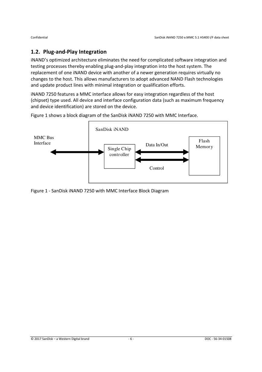
Figure 1 shows a block diagram of the SanDisk iNAND 7250 with MMC Interface.
MMC Bus
Interface
SanDisk iNAND
Single Chip
controller
Data In/Out
Flash
Memory
Control
Figure 1 - SanDisk iNAND 7250 with MMC Interface Block Diagram
© 2017 SanDisk – a Western Digital brand
- 6 -
DOC - 56-34-01508
�
Confidential
SanDisk iNAND 7250 e.MMC 5.1 HS400 I/F data sheet
1.3. Feature Overview
SanDisk iNAND 7250, with MMC interface, includes the following features:
• Memory controller and NAND flash
• Mechanical design that complies with JEDEC Specifications with specific optimizations for
automotive applications
• Offered in three TFBGA packages of e.MMC 5.1
o 11.5mm x 13mm x 0.8mm (8GB-16GB)
o 11.5mm x 13mm x 1.0mm (32GB)
o 11.5mm x 13mm x 1.2mm (64GB)
• Operating temperature range: –25C° to +85C°
• Dual power system
• Core voltage (VCC) 2.7-3.6 V
•
I/O (VCCQ) voltage, either: 1.7-1.95V or 2.7-3.6V
• 8GB - 64GB of data storage
• Supports three data bus widths: 1bit (default), 4bit, 8bit
• Complies with e.MMC Specification Ver. 5.1 HS400
• Variable clock frequencies of 0-20 MHz, 0-26 MHz (default), 0-52 MHz (high-speed), 0-200
MHz SDR (HS200), 0-200 MHz DDR (HS400)
• Up to 300 MB/sec bus transfer rate, using 8 parallel data lines at 200 MHz, HS400 Mode
• High data integrity with eMLC memory, advanced LDPC ECC engine, automatic refresh,
advanced power protection
• Flexible EUDA, Fast boot
• Up to 3K P/E cycles, 10 year data retention @ 55°C fresh
© 2017 SanDisk – a Western Digital brand
- 7 -
DOC - 56-34-01508
�
Confidential
SanDisk iNAND 7250 e.MMC 5.1 HS400 I/F data sheet
1.4. MMC bus and Power Lines
SanDisk iNAND 7250 supports the MMC interface protocol. For more details regarding these
buses refer to JEDEC standard No. JESD84-B51.
The iNAND bus has the following communication and power lines:
• CMD: Command is a bidirectional signal. The host and iNAND operate in two modes, open
drain and push-pull.
• DAT0-7: Data lines are bidirectional signals. Host and iNAND operate in push-pull mode.
• CLK: Clock input.
• RST_n: Hardware Reset Input.
• VCCQ: Power supply line for host interface.
• VCC: Power supply line for internal flash memory.
• VDDi: iNAND’s internal power node, not the power supply. Connect 0.1uF capacitor from
VDDi to ground.
• VSS, VSSQ: Ground lines.
• RCLK: Data strobe.
• VSF: Vendor specific functions used for debugging purposes.
1.4.1. Bus operating conditions
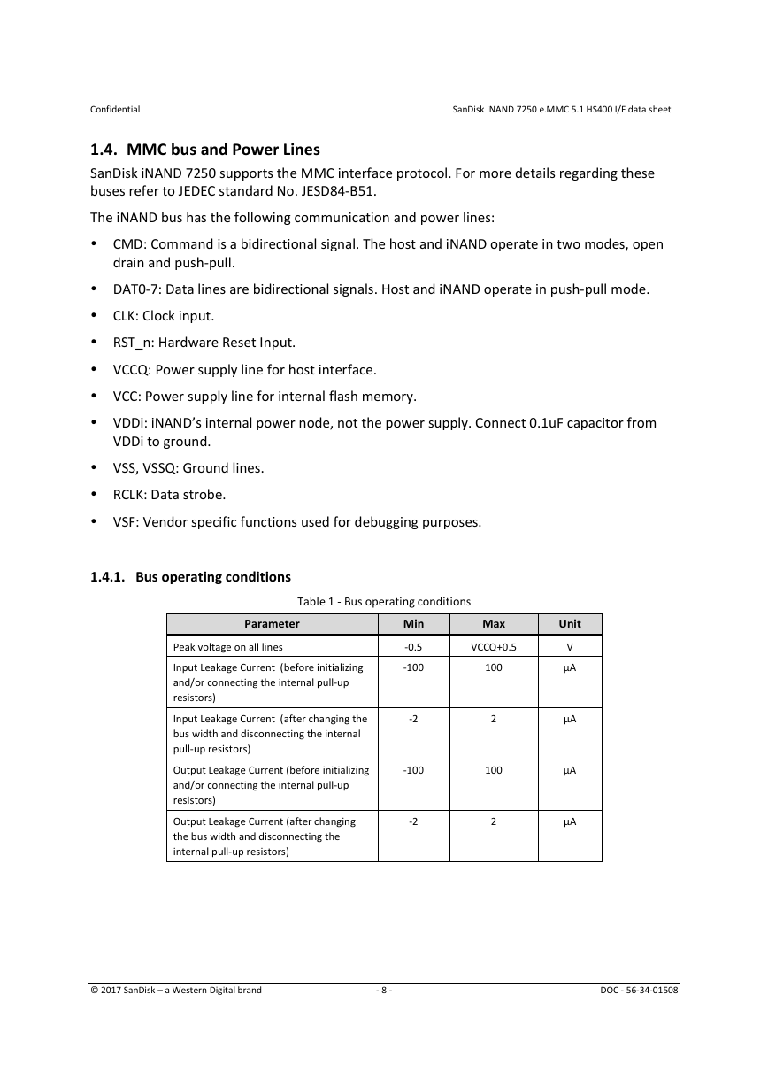
Table 1 - Bus operating conditions
Max
Unit
VCCQ+0.5
100
V
µA
µA
Parameter
Peak voltage on all lines
Input Leakage Current (before initializing
and/or connecting the internal pull-up
resistors)
Min
-0.5
-100
Input Leakage Current (after changing the
-2
2
bus width and disconnecting the internal
pull-up resistors)
Output Leakage Current (before initializing
and/or connecting the internal pull-up
resistors)
-100
100
µA
Output Leakage Current (after changing
-2
2
µA
the bus width and disconnecting the
internal pull-up resistors)
© 2017 SanDisk – a Western Digital brand
- 8 -
DOC - 56-34-01508
�



 2023年江西萍乡中考道德与法治真题及答案.doc
 2012年重庆南川中考生物真题及答案.doc
 2013年江西师范大学地理学综合及文艺理论基础考研真题.doc
 2020年四川甘孜小升初语文真题及答案I卷.doc
 2020年注册岩土工程师专业基础考试真题及答案.doc
 2023-2024学年福建省厦门市九年级上学期数学月考试题及答案.doc
 2021-2022学年辽宁省沈阳市大东区九年级上学期语文期末试题及答案.doc
 2022-2023学年北京东城区初三第一学期物理期末试卷及答案.doc
 2018上半年江西教师资格初中地理学科知识与教学能力真题及答案.doc
 2012年河北国家公务员申论考试真题及答案-省级.doc
 2020-2021学年江苏省扬州市江都区邵樊片九年级上学期数学第一次质量检测试题及答案.doc
 2022下半年黑龙江教师资格证中学综合素质真题及答案.doc