Lontium Semiconductor
LT8918L Datasheet R1.4
LONTIUM SEMICONDUCTOR
CORPORATION
ClearEdge Technology
LT8918L
Datasheet
Dual-Port LVDS to MIPI DSI/CSI-2 Bridge
We produce mixed-signal products for a better digital world!
Confidential
1
�
Lontium Semiconductor
LT8918L Datasheet R1.4
1. Features
Single/Dual-Port LVDS Receiver
External 25MHz Crystal Reference Clock
Temperature Range: -40°C to +85°C
Packaged in QFN64 7.5mm x 7.5mm and BGA81 5mm
Compatible with VESA and JEIDA standard
1~2 Configurable Port
1 Clock Lane and Up to 5 Data Lanes per Port
Data Lane and Polarity Swapping
Support Maximum Data Rate 1.2Gb/s/lane
Resolution up to 1080P 60Hz for Dual-Port Mode
Input Color Depth Supports 6-bit, 8-bit and 10-bit
Support Input De-SSC (30kHz±5%)
Single-Port MIPI DSI Transmitter
Compliant with DCS1.02, D-PHY1.1 & DSI1.02
1 Clock Lane and 1~4 Configurable Data Lanes
80Mb/s~1.5Gb/s per Data Lane
Resolution Up to 1080P 60Hz
Data Lane and Polarity Swapping
Both Non-Burst and Burst Video Mode Supported
Command Mode through Lane-0 Supported
Support RGB666, Loosely RGB666, RGB888, RGB565,
16-bit YCbCr4:2:2, 24-bit YCbCr 4:2:2 Video Format
Single-Port MIPI CSI-2 Transmitter
Compliant with D-PHY1.1 & CSI-2 1.0
1 Clock Lane and 1~4 Configurable Data Lanes
80Mb/s~1.5Gb/s per Data Lane
Resolution Up to 1080P 60Hz
Data Lane and Polarity Swapping
Support RGB565, RGB666, RGB888, 8-bit YUV422
Video Format
Miscellaneous
1.8V Single Supply Power
Support 100KHz and 400KHz I2C slave
Support SPI slave
x 5mm
2. General Description
The Lontium LT8918L is a high performance Dual-Port LVDS
to MIPIDSI/CSI-2 bridge chip between AP and mobile display
panel or camera .
LT8918L can be configured as single-port or dual-port with
optional De-SSC function. The bridge deserializes input
LVDS data, decodes packets and converts the formatted
video data stream to MIPIDSI/CSI-2 transmitter output.
For MIPI DSI/CSI-2 output, LT8918L features a single port
MIPI DSI or CSI-2 transmitter with 1 high-speed clock lane
and 1~4 configurable high-speed data lanes operating at
maximum 1.5Gb/s/lane, which can support a total bandwidth
of up to 6Gb/s. LT8918L supports both Non-Burst and Burst
DSI video data transferring, as well as Command Mode
through Lane-0.
The LT8918L is fabricated in advanced CMOS process and
implemented in a small outline 7.5mm x 7.5mm QFN64
package. This package is RoHS compliant and specified to
operate from -40°C to +85°C.
3. Applications
Mobile systems
Cellular handsets
Digital video cameras
Digital still cameras
Tablet PC, Notebook PC
Car Display and Camera System
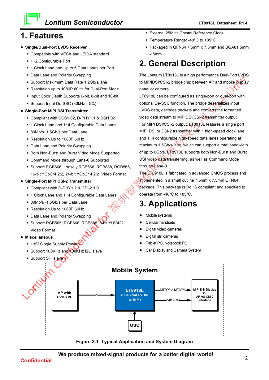
Mobile System
AP with
LVDS I/F
LT8918L
(Dual-Port LVDS-
to-MIPI)
MT0P/N~MT3P/N
MTCP/N
MIPI DSI Display
Or
AP w/i CSI-2
Interface
OSC
Figure 3.1 Typical Application and System Diagram
We produce mixed-signal products for a better digital world!
Confidential
2
�
Lontium Semiconductor
LT8918L Datasheet R1.4
4. Ordering Information
Table 4.1 Ordering Information
Part Number
Operating
Temperature Range
Package
Packing Method
LT8918L
−40°C to +85°C
QFN64 (7.5*7.5)/BGA81 (5*5)
Tray
We produce mixed-signal products for a better digital world!
Confidential
3
�
Lontium Semiconductor
LT8918L Datasheet R1.4
Table of Contents
1. Features ................................................................................................................................ 2
2. General Description ............................................................................................................. 2
3. Applications .......................................................................................................................... 2
4. Ordering Information ........................................................................................................... 3
5. Revision History ................................................................................................................... 5
6. Pinning Information ............................................................................................................. 6
6.1 QFN64 Pin Diagram ......................................................................................................... 6
6.2 QFN64 Pin Description ..................................................................................................... 7
6.3 BGA81 Ball Map ............................................................................................................. 11
6.4 BGA81 Ball Description .................................................................................................. 12
7. Function Block Diagram .................................................................................................... 16
8. Electrical Characteristics .................................................................................................. 17
8.1 Absolute Maximum Conditions ....................................................................................... 17
8.2 Normal Operating Conditions.......................................................................................... 17
8.3 DC Characteristics .......................................................................................................... 17
8.4 AC Characteristics .......................................................................................................... 18
9. Package Information .......................................................................................................... 19
9.1 QFN64 7.5mm x 7.5mm Package ................................................................................... 19
9.2 BGA81 5mm x 5mm Package ......................................................................................... 20
We produce mixed-signal products for a better digital world!
Confidential
4
�
Lontium Semiconductor
LT8918L Datasheet R1.4
5. Revision History
Version Owner
Content
Date
R1.0
R1.1
R1.2
R1.3
R1.4
C T
N W
C T
C T
Initial Release
Change package information
1. Update pin/ball name: LB3N/P LBCN/P, LB4N/P
LB3N/P
Modify the format of the document
1. Update pin direction description for BGA81 package
2. Update speed description in both pin definition
sections
08/16/2016
08/18/2016
09/13/2016
06/01/2017
08/24/2017
We produce mixed-signal products for a better digital world!
Confidential
5
�
Lontium Semiconductor
LT8918L Datasheet R1.4
6. Pinning Information
To improve signal integrity, all differential pairs should be routed with 100Ω±10% differential impedance. Maximum trace length
mismatch should be less than 5mil and keep total trace length to a minimum for all differential traces. Routing differential pairs on
the top or bottom layer with no vias as on signal path is highly recommended.
For crystal oscillator, keep XTALI/XTALO as short as possible and away from noisy signal source. Minimize parasitic
capacitances on these two pins and shield them with clean ground lines.
To minimize the power supply noise floor, at least one 0.1μF and one 0.01μF decoupling capacitor is recommended to be
installed near all the LT8918L 1.8V power pins. To avoid large current loops and trace inductance, the trace length between
decoupling capacitor and device power inputs pins must be minimized.
6.1 QFN64 Pin Diagram
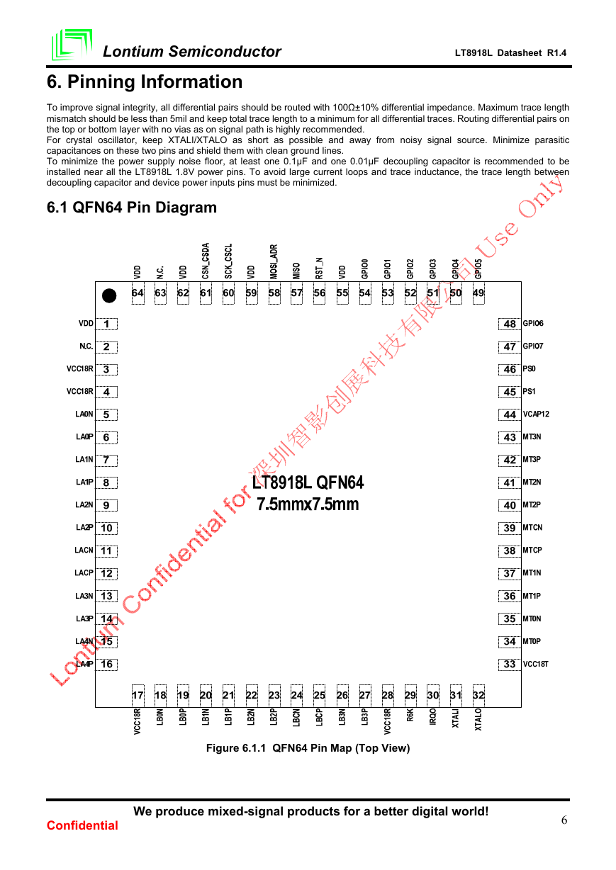
Figure 6.1.1 QFN64 Pin Map (Top View)
We produce mixed-signal products for a better digital world!
Confidential
6
�
Lontium Semiconductor
LT8918L Datasheet R1.4
6.2 QFN64 Pin Description
Pin No.
Pin Name
Pin Description
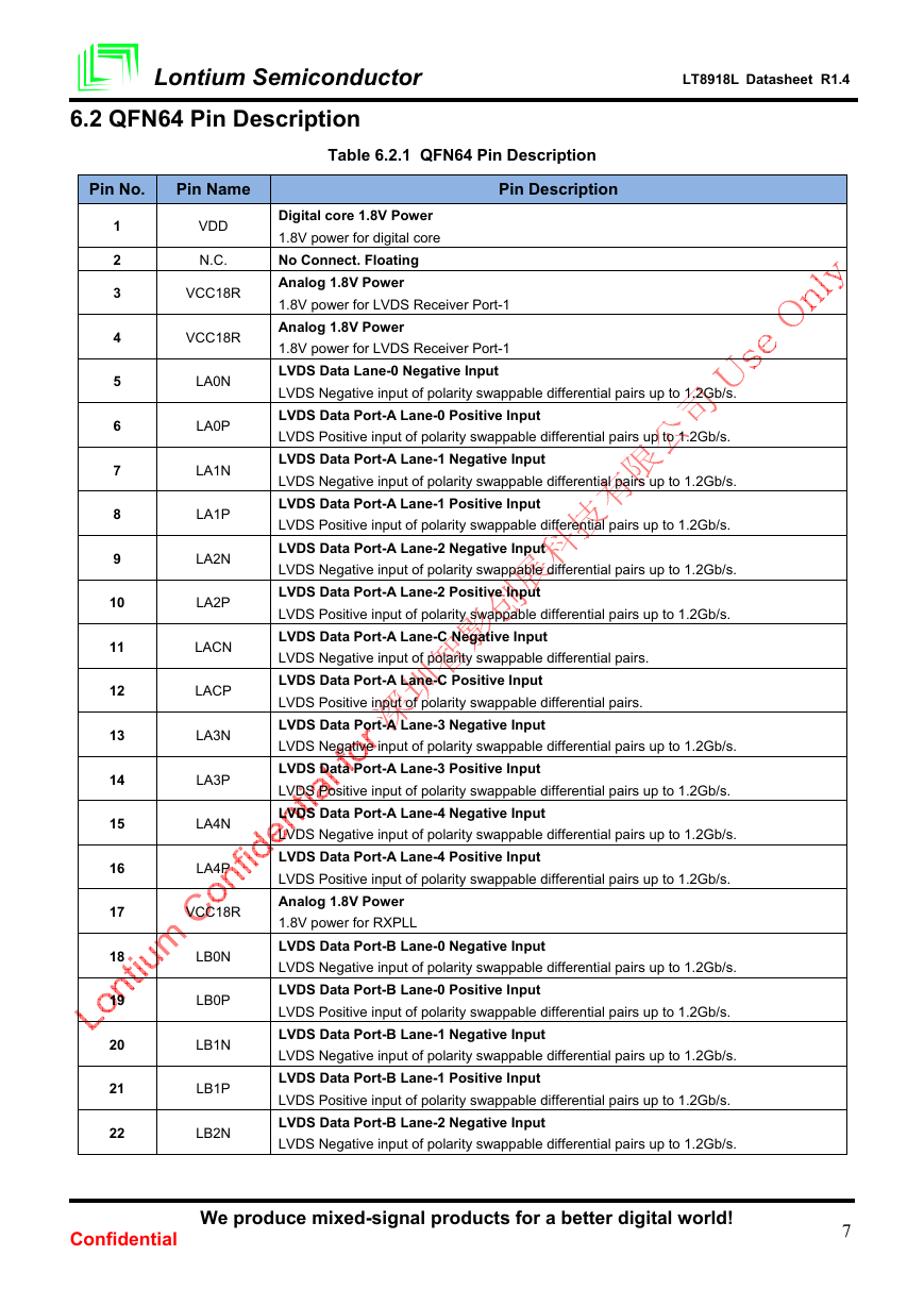
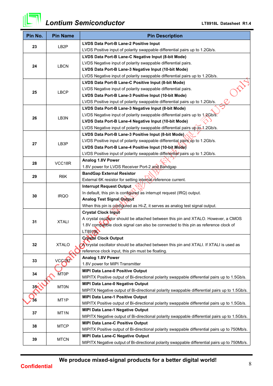
Table 6.2.1 QFN64 Pin Description
1
2
3
4
5
6
7
8
9
10
11
12
13
14
15
16
17
18
19
20
21
22
VDD
N.C.
VCC18R
VCC18R
LA0N
LA0P
LA1N
LA1P
LA2N
LA2P
LACN
LACP
LA3N
LA3P
LA4N
LA4P
VCC18R
LB0N
LB0P
LB1N
LB1P
LB2N
Digital core 1.8V Power
1.8V power for digital core
No Connect. Floating
Analog 1.8V Power
1.8V power for LVDS Receiver Port-1
Analog 1.8V Power
1.8V power for LVDS Receiver Port-1
LVDS Data Lane-0 Negative Input
LVDS Negative input of polarity swappable differential pairs up to 1.2Gb/s.
LVDS Data Port-A Lane-0 Positive Input
LVDS Positive input of polarity swappable differential pairs up to 1.2Gb/s.
LVDS Data Port-A Lane-1 Negative Input
LVDS Negative input of polarity swappable differential pairs up to 1.2Gb/s.
LVDS Data Port-A Lane-1 Positive Input
LVDS Positive input of polarity swappable differential pairs up to 1.2Gb/s.
LVDS Data Port-A Lane-2 Negative Input
LVDS Negative input of polarity swappable differential pairs up to 1.2Gb/s.
LVDS Data Port-A Lane-2 Positive Input
LVDS Positive input of polarity swappable differential pairs up to 1.2Gb/s.
LVDS Data Port-A Lane-C Negative Input
LVDS Negative input of polarity swappable differential pairs.
LVDS Data Port-A Lane-C Positive Input
LVDS Positive input of polarity swappable differential pairs.
LVDS Data Port-A Lane-3 Negative Input
LVDS Negative input of polarity swappable differential pairs up to 1.2Gb/s.
LVDS Data Port-A Lane-3 Positive Input
LVDS Positive input of polarity swappable differential pairs up to 1.2Gb/s.
LVDS Data Port-A Lane-4 Negative Input
LVDS Negative input of polarity swappable differential pairs up to 1.2Gb/s.
LVDS Data Port-A Lane-4 Positive Input
LVDS Positive input of polarity swappable differential pairs up to 1.2Gb/s.
Analog 1.8V Power
1.8V power for RXPLL
LVDS Data Port-B Lane-0 Negative Input
LVDS Negative input of polarity swappable differential pairs up to 1.2Gb/s.
LVDS Data Port-B Lane-0 Positive Input
LVDS Positive input of polarity swappable differential pairs up to 1.2Gb/s.
LVDS Data Port-B Lane-1 Negative Input
LVDS Negative input of polarity swappable differential pairs up to 1.2Gb/s.
LVDS Data Port-B Lane-1 Positive Input
LVDS Positive input of polarity swappable differential pairs up to 1.2Gb/s.
LVDS Data Port-B Lane-2 Negative Input
LVDS Negative input of polarity swappable differential pairs up to 1.2Gb/s.
We produce mixed-signal products for a better digital world!
Confidential
7
�
LT8918L Datasheet R1.4
Lontium Semiconductor
Pin No.
Pin Name
Pin Description
23
24
25
26
27
28
29
30
31
32
33
34
35
36
37
38
39
LB2P
LBCN
LBCP
LB3N
LB3P
VCC18R
R6K
IRQO
XTALI
XTALO
VCC18T
MT0P
MT0N
MT1P
MT1N
MTCP
MTCN
LVDS Data Port-B Lane-2 Positive Input
LVDS Positive input of polarity swappable differential pairs up to 1.2Gb/s.
LVDS Data Port-B Lane-C Negative Input (8-bit Mode)
LVDS Negative input of polarity swappable differential pairs.
LVDS Data Port-B Lane-3 Negative Input (10-bit Mode)
LVDS Negative input of polarity swappable differential pairs up to 1.2Gb/s.
LVDS Data Port-B Lane-C Positive Input (8-bit Mode)
LVDS Negative input of polarity swappable differential pairs.
LVDS Data Port-B Lane-3 Positive Input (10-bit Mode)
LVDS Positive input of polarity swappable differential pairs up to 1.2Gb/s.
LVDS Data Port-B Lane-3 Negative Input (8-bit Mode)
LVDS Negative input of polarity swappable differential pairs up to 1.2Gb/s.
LVDS Data Port-B Lane-4 Negative Input (10-bit Mode)
LVDS Negative input of polarity swappable differential pairs up to 1.2Gb/s.
LVDS Data Port-B Lane-3 Positive Input (8-bit Mode)
LVDS Positive input of polarity swappable differential pairs up to 1.2Gb/s.
LVDS Data Port-B Lane-4 Positive Input (10-bit Mode)
LVDS Positive input of polarity swappable differential pairs up to 1.2Gb/s.
Analog 1.8V Power
1.8V power for LVDS Receiver Port-2 and Bandgap
BandGap External Resistor
External 6K resistor for setting internal reference current.
Interrupt Request Output
In default, this pin is configured as interrupt request (IRQ) output.
Analog Test Signal Output
When this pin is configured as Hi-Z, it serves as analog test signal output.
Crystal Clock Input
A crystal oscillator should be attached between this pin and XTALO. However, a CMOS
1.8V compatible clock signal can also be connected to this pin as reference clock of
LT8918L
Crystal Clock Output
A crystal oscillator should be attached between this pin and XTALI. If XTALI is used as
reference clock input, this pin must be floating.
Analog 1.8V Power
1.8V power for MIPI Transmitter
MIPI Data Lane-0 Positive Output
MIPITX Positive output of Bi-directional polarity swappable differential pairs up to 1.5Gb/s.
MIPI Data Lane-0 Negative Output
MIPITX Negative output of Bi-directional polarity swappable differential pairs up to 1.5Gb/s.
MIPI Data Lane-1 Positive Output
MIPITX Positive output of Bi-directional polarity swappable differential pairs up to 1.5Gb/s.
MIPI Data Lane-1 Negative Output
MIPITX Negative output of Bi-directional polarity swappable differential pairs up to 1.5Gb/s.
MIPI Data Lane-C Positive Output
MIPITX Positive output of Bi-directional polarity swappable differential pairs up to 750Mb/s.
MIPI Data Lane-C Negative Output
MIPITX Negative output of Bi-directional polarity swappable differential pairs up to 750Mb/s.
We produce mixed-signal products for a better digital world!
Confidential
8
�



 2023年江西萍乡中考道德与法治真题及答案.doc
 2012年重庆南川中考生物真题及答案.doc
 2013年江西师范大学地理学综合及文艺理论基础考研真题.doc
 2020年四川甘孜小升初语文真题及答案I卷.doc
 2020年注册岩土工程师专业基础考试真题及答案.doc
 2023-2024学年福建省厦门市九年级上学期数学月考试题及答案.doc
 2021-2022学年辽宁省沈阳市大东区九年级上学期语文期末试题及答案.doc
 2022-2023学年北京东城区初三第一学期物理期末试卷及答案.doc
 2018上半年江西教师资格初中地理学科知识与教学能力真题及答案.doc
 2012年河北国家公务员申论考试真题及答案-省级.doc
 2020-2021学年江苏省扬州市江都区邵樊片九年级上学期数学第一次质量检测试题及答案.doc
 2022下半年黑龙江教师资格证中学综合素质真题及答案.doc