6 ■
Solutions to Case Studies and Exercises
Chapter 2 Solutions
Case Study 1: Optimizing Cache Performance via
Advanced Techniques
2.1
a. Each element is 8B. Since a 64B cacheline has 8 elements, and each column
access will result in fetching a new line for the non-ideal matrix, we need a
minimum of 8x8 (64 elements) for each matrix. Hence, the minimum cache
size is 128 × 8B = 1KB.
b. The blocked version only has to fetch each input and output element once.
The unblocked version will have one cache miss for every 64B/8B = 8 row
elements. Each column requires 64Bx256 of storage, or 16KB. Thus, column
elements will be replaced in the cache before they can be used again. Hence
the unblocked version will have 9 misses (1 row and 8 columns) for every 2 in
the blocked version.
c. for (i = 0; i < 256; i=i+B) {
for (j = 0; j < 256; j=j+B) {
for(m=0; m
Chapter 2 Solutions
■ 7
Case Study 2: Putting it all Together: Highly Parallel
Memory Systems
2.4
a. The second-level cache is 1MB and has a 128B block size.
b. The miss penalty of the second-level cache is approximately 105ns.
c. The second-level cache is 8-way set associative.
d. The main memory is 512MB.
e. Walking through pages with a 16B stride takes 946ns per reference. With 250
such references per page, this works out to approximately 240ms per page.
2.5
a. Hint: This is visible in the graph above as a slight increase in L2 miss service
time for large data sets, and is 4KB for the graph above.
b. Hint: Take independent strides by the page size and look for increases in
latency not attributable to cache sizes. This may be hard to discern if the
amount of memory mapped by the TLB is almost the same as the size as a
cache level.
c. Hint: This is visible in the graph above as a slight increase in L2 miss service
time for large data sets, and is 15ns in the graph above.
d. Hint: Take independent strides that are multiples of the page size to see if the
TLB if fully-associative or set-associative. This may be hard to discern if the
amount of memory mapped by the TLB is almost the same as the size as a
cache level.
2.6
a. Hint: Look at the speed of programs that easily fit in the top-level cache as a
function of the number of threads.
b. Hint: Compare the performance of independent references as a function of
their placement in memory.
2.7 Open hands-on exercise, no fixed solution.
Exercises
2.8
a. The access time of the direct-mapped cache is 0.86ns, while the 2-way and
4-way are 1.12ns and 1.37ns respectively. This makes the relative access
times 1.12/.86 = 1.30 or 30% more for the 2-way and 1.37/0.86 = 1.59 or
59% more for the 4-way.
b. The access time of the 16KB cache is 1.27ns, while the 32KB and 64KB are
1.35ns and 1.37ns respectively. This makes the relative access times 1.35/
1.27 = 1.06 or 6% larger for the 32KB and 1.37/1.27 = 1.078 or 8% larger for
the 64KB.
c. Avg. access time = hit% × hit time + miss% × miss penalty, miss% = misses
per instruction/references per instruction = 2.2% (DM), 1.2% (2-way), 0.33%
(4-way), .09% (8-way).
Direct mapped access time = .86ns @ .5ns cycle time = 2 cycles
2-way set associative = 1.12ns @ .5ns cycle time = 3 cycles
Copyright © 2012 Elsevier, Inc. All rights reserved.�
8 ■
Solutions to Case Studies and Exercises
2.9
4-way set associative = 1.37ns @ .83ns cycle time = 2 cycles
8-way set associative = 2.03ns @ .79ns cycle time = 3 cycles
Miss penalty = (10/.5) = 20 cycles for DM and 2-way; 10/.83 = 13 cycles for
4-way; 10/.79 = 13 cycles for 8-way.
Direct mapped – (1 – .022) × 2 + .022 × (20) = 2.39 6 cycles => 2.396 × .5 = 1.2ns
2-way – (1 – .012) × 3 + .012 × (20) = 3. 2 cycles => 3.2 × .5 = 1.6ns
4-way – (1 – .0033) × 2 + .0033 × (13) = 2.036 cycles => 2.06 × .83 = 1.69ns
8-way – (1 – .0009) × 3 + .0009 × 13 = 3 cycles => 3 × .79 = 2.37ns
Direct mapped cache is the best.
a. The average memory access time of the current (4-way 64KB) cache is 1.69ns.
64KB direct mapped cache access time = .86ns @ .5 ns cycle time = 2 cycles
Way-predicted cache has cycle time and access time similar to direct mapped
cache and miss rate similar to 4-way cache.
The AMAT of the way-predicted cache has three components: miss, hit with
way prediction correct, and hit with way prediction mispredict: 0.0033 × (20)
+ (0.80 × 2 + (1 – 0.80) × 3) × (1 – 0.0033) = 2.26 cycles = 1.13ns
b. The cycle time of the 64KB 4-way cache is 0.83ns, while the 64KB direct-
mapped cache can be accessed in 0.5ns. This provides 0.83/0.5 = 1.66 or 66%
faster cache access.
c. With 1 cycle way misprediction penalty, AMAT is 1.13ns (as per part a), but
with a 15 cycle misprediction penalty, the AMAT becomes: 0.0033 × 20 +
(0.80 × 2 + (1 – 0.80) × 15) × (1 – 0.0033) = 4.65 cycles or 2.3ns.
d. The serial access is 2.4ns/1.59ns = 1.509 or 51% slower.
a. The access time is 1.12ns, while the cycle time is 0.51ns, which could be
2.10
potentially pipelined as finely as 1.12/.51 = 2.2 pipestages.
2.11
b. The pipelined design (not including latch area and power) has an area of
1.19 mm2 and energy per access of 0.16nJ. The banked cache has an area of
1.36 mm2 and energy per access of 0.13nJ. The banked design uses slightly
more area because it has more sense amps and other circuitry to support the
two banks, while the pipelined design burns slightly more power because the
memory arrays that are active are larger than in the banked case.
b.
a. With critical word first, the miss service would require 120 cycles. Without
critical word first, it would require 120 cycles for the first 16B and 16 cycles
for each of the next 3 16B blocks, or 120 + (3 × 16) = 168 cycles.
It depends on the contribution to Average Memory Access Time (AMAT) of
the level-1 and level-2 cache misses and the percent reduction in miss service
times provided by critical word first and early restart. If the percentage reduc-
tion in miss service times provided by critical word first and early restart is
roughly the same for both level-1 and level-2 miss service, then if level-1
misses contribute more to AMAT, critical word first would likely be more
important for level-1 misses.
Copyright © 2012 Elsevier, Inc. All rights reserved.�
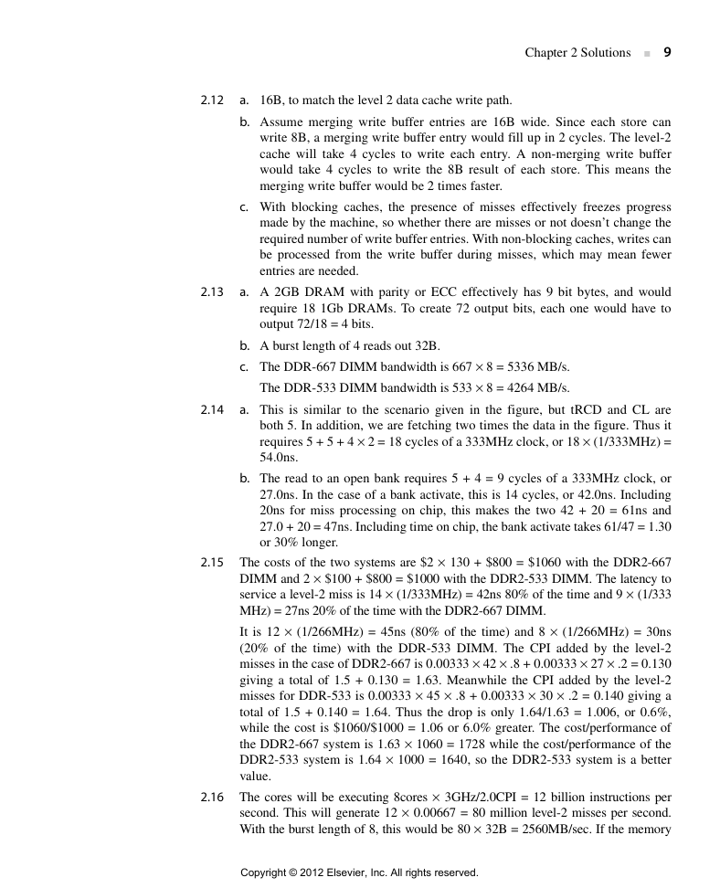
Chapter 2 Solutions
■ 9
2.12
a. 16B, to match the level 2 data cache write path.
b. Assume merging write buffer entries are 16B wide. Since each store can
write 8B, a merging write buffer entry would fill up in 2 cycles. The level-2
cache will take 4 cycles to write each entry. A non-merging write buffer
would take 4 cycles to write the 8B result of each store. This means the
merging write buffer would be 2 times faster.
c. With blocking caches, the presence of misses effectively freezes progress
made by the machine, so whether there are misses or not doesn’t change the
required number of write buffer entries. With non-blocking caches, writes can
be processed from the write buffer during misses, which may mean fewer
entries are needed.
2.13
a. A 2GB DRAM with parity or ECC effectively has 9 bit bytes, and would
require 18 1Gb DRAMs. To create 72 output bits, each one would have to
output 72/18 = 4 bits.
b. A burst length of 4 reads out 32B.
c. The DDR-667 DIMM bandwidth is 667 × 8 = 5336 MB/s.
The DDR-533 DIMM bandwidth is 533 × 8 = 4264 MB/s.
2.14
a. This is similar to the scenario given in the figure, but tRCD and CL are
both 5. In addition, we are fetching two times the data in the figure. Thus it
requires 5 + 5 + 4 × 2 = 18 cycles of a 333MHz clock, or 18 × (1/333MHz) =
54.0ns.
b. The read to an open bank requires 5 + 4 = 9 cycles of a 333MHz clock, or
27.0ns. In the case of a bank activate, this is 14 cycles, or 42.0ns. Including
20ns for miss processing on chip, this makes the two 42 + 20 = 61ns and
27.0 + 20 = 47ns. Including time on chip, the bank activate takes 61/47 = 1.30
or 30% longer.
2.15 The costs of the two systems are $2 × 130 + $800 = $1060 with the DDR2-667
DIMM and 2 × $100 + $800 = $1000 with the DDR2-533 DIMM. The latency to
service a level-2 miss is 14 × (1/333MHz) = 42ns 80% of the time and 9 × (1/333
MHz) = 27ns 20% of the time with the DDR2-667 DIMM.
It is 12 × (1/266MHz) = 45ns (80% of the time) and 8 × (1/266MHz) = 30ns
(20% of the time) with the DDR-533 DIMM. The CPI added by the level-2
misses in the case of DDR2-667 is 0.00333 × 42 × .8 + 0.00333 × 27 × .2 = 0.130
giving a total of 1.5 + 0.130 = 1.63. Meanwhile the CPI added by the level-2
misses for DDR-533 is 0.00333 × 45 × .8 + 0.00333 × 30 × .2 = 0.140 giving a
total of 1.5 + 0.140 = 1.64. Thus the drop is only 1.64/1.63 = 1.006, or 0.6%,
while the cost is $1060/$1000 = 1.06 or 6.0% greater. The cost/performance of
the DDR2-667 system is 1.63 × 1060 = 1728 while the cost/performance of the
DDR2-533 system is 1.64 × 1000 = 1640, so the DDR2-533 system is a better
value.
2.16 The cores will be executing 8cores × 3GHz/2.0CPI = 12 billion instructions per
second. This will generate 12 × 0.00667 = 80 million level-2 misses per second.
With the burst length of 8, this would be 80 × 32B = 2560MB/sec. If the memory
Copyright © 2012 Elsevier, Inc. All rights reserved.�
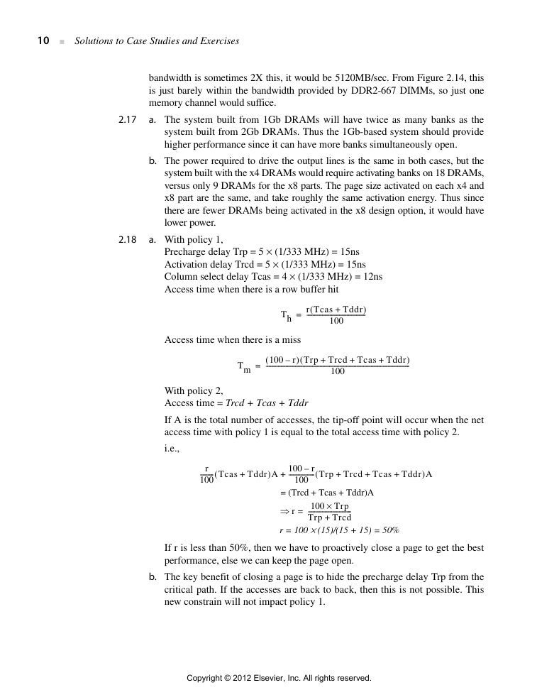
10 ■
Solutions to Case Studies and Exercises
2.17
bandwidth is sometimes 2X this, it would be 5120MB/sec. From Figure 2.14, this
is just barely within the bandwidth provided by DDR2-667 DIMMs, so just one
memory channel would suffice.
a. The system built from 1Gb DRAMs will have twice as many banks as the
system built from 2Gb DRAMs. Thus the 1Gb-based system should provide
higher performance since it can have more banks simultaneously open.
b. The power required to drive the output lines is the same in both cases, but the
system built with the x4 DRAMs would require activating banks on 18 DRAMs,
versus only 9 DRAMs for the x8 parts. The page size activated on each x4 and
x8 part are the same, and take roughly the same activation energy. Thus since
there are fewer DRAMs being activated in the x8 design option, it would have
lower power.
2.18
a. With policy 1,
Precharge delay Trp = 5 × (1/333 MHz) = 15ns
Activation delay Trcd = 5 × (1/333 MHz) = 15ns
Column select delay Tcas = 4 × (1/333 MHz) = 12ns
Access time when there is a row buffer hit
Th
=
)
(
r Tcas Tddr
--------------------------------------
+
100
Access time when there is a miss
)
) Trp Trcd Tcas Tddr
(
(
100 r–
---------------------------------------------------------------------------------------------
+
+
+
=
Tm
100
With policy 2,
Access time = Trcd + Tcas + Tddr
If A is the total number of accesses, the tip-off point will occur when the net
access time with policy 1 is equal to the total access time with policy 2.
i.e.,
r
(
--------- Tcas Tddr
100
+
)A
+
100
----------------- Trp Trcd Tcas Tddr
r–
+
+
+
(
100
)A
= (Trcd + Tcas + Tddr)A
×
+
r
100 Trp
----------------------------
Trp Trcd
=⇒
r = 100 × (15)/(15 + 15) = 50%
If r is less than 50%, then we have to proactively close a page to get the best
performance, else we can keep the page open.
b. The key benefit of closing a page is to hide the precharge delay Trp from the
critical path. If the accesses are back to back, then this is not possible. This
new constrain will not impact policy 1.
Copyright © 2012 Elsevier, Inc. All rights reserved.�
Chapter 2 Solutions
■ 11
The new equations for policy 2,
Access time when we can hide precharge delay = Trcd + Tcas + Tddr
Access time when precharge delay is in the critical path = Trcd + Tcas + Trp + Tddr
Equation 1 will now become,
(
r
--------- Tcas Tddr
100
=
)A 100 r–
100
+
Trcd Tcas Tddr
0.9
×
+
+
+
(
)
(
----------------- Trp Trcd Tcas Tddr
+
+
+
)A
A 0.1
+
×
(
Trcd Tcas Trp Tddr
+
+
+
)
=
×
90
Trp
r⇒
+
r = 90 × 15/30 = 45%
⎞
----------------------------
⎠
Trp Trcd
⎛
⎝
c. For any row buffer hit rate, policy 2 requires additional r × (2 + 4) nJ per
access. If r = 50%, then policy 2 requires 3nJ of additional energy.
2.19 Hibernating will be useful when the static energy saved in DRAM is at least equal
to the energy required to copy from DRAM to Flash and then back to DRAM.
DRAM dynamic energy to read/write is negligible compared to Flash and can be
ignored.
Time
=
×
109
10 6–
8
-------------------------------------------------------------
××
2
64
2.56
1.6×
×
= 400 seconds
The factor 2 in the above equation is because to hibernate and wakeup, both Flash
and DRAM have to be read and written once.
a. Yes. The application and production environment can be run on a VM hosted
2.20
on a development machine.
b. Yes. Applications can be redeployed on the same environment on top of VMs
running on different hardware. This is commonly called business continuity.
c. No. Depending on support in the architecture, virtualizing I/O may add sig-
nificant or very significant performance overheads.
d. Yes. Applications running on different virtual machines are isolated from
each other.
e. Yes. See “Devirtualizable virtual machines enabling general, single-node,
online maintenance,” David Lowell, Yasushi Saito, and Eileen Samberg, in
the Proceedings of the 11th ASPLOS, 2004, pages 211–223.
2.21
a. Programs that do a lot of computation but have small memory working sets
and do little I/O or other system calls.
b. The slowdown above was 60% for 10%, so 20% system time would run
120% slower.
c. The median slowdown using pure virtualization is 10.3, while for para virtu-
alization the median slowdown is 3.76.
Copyright © 2012 Elsevier, Inc. All rights reserved.�
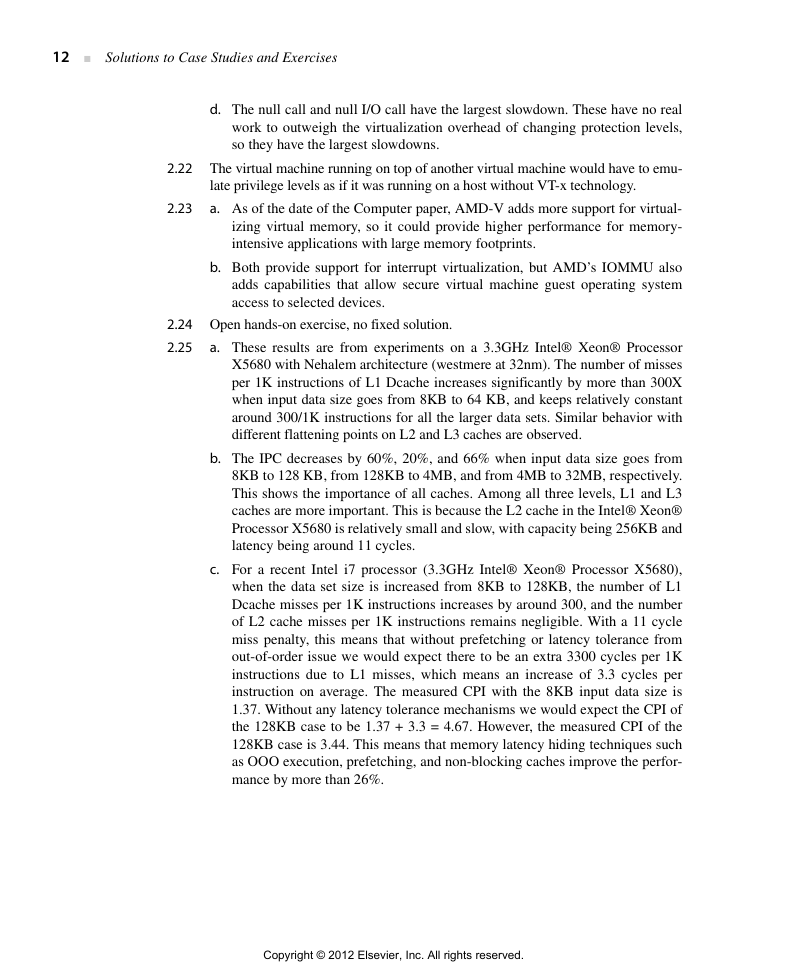
12 ■
Solutions to Case Studies and Exercises
d. The null call and null I/O call have the largest slowdown. These have no real
work to outweigh the virtualization overhead of changing protection levels,
so they have the largest slowdowns.
2.22 The virtual machine running on top of another virtual machine would have to emu-
2.23
late privilege levels as if it was running on a host without VT-x technology.
a. As of the date of the Computer paper, AMD-V adds more support for virtual-
izing virtual memory, so it could provide higher performance for memory-
intensive applications with large memory footprints.
b. Both provide support for interrupt virtualization, but AMD’s IOMMU also
adds capabilities that allow secure virtual machine guest operating system
access to selected devices.
2.24 Open hands-on exercise, no fixed solution.
2.25
a. These results are from experiments on a 3.3GHz Intel® Xeon® Processor
X5680 with Nehalem architecture (westmere at 32nm). The number of misses
per 1K instructions of L1 Dcache increases significantly by more than 300X
when input data size goes from 8KB to 64 KB, and keeps relatively constant
around 300/1K instructions for all the larger data sets. Similar behavior with
different flattening points on L2 and L3 caches are observed.
b. The IPC decreases by 60%, 20%, and 66% when input data size goes from
8KB to 128 KB, from 128KB to 4MB, and from 4MB to 32MB, respectively.
This shows the importance of all caches. Among all three levels, L1 and L3
caches are more important. This is because the L2 cache in the Intel® Xeon®
Processor X5680 is relatively small and slow, with capacity being 256KB and
latency being around 11 cycles.
c. For a recent Intel i7 processor (3.3GHz Intel® Xeon® Processor X5680),
when the data set size is increased from 8KB to 128KB, the number of L1
Dcache misses per 1K instructions increases by around 300, and the number
of L2 cache misses per 1K instructions remains negligible. With a 11 cycle
miss penalty, this means that without prefetching or latency tolerance from
out-of-order issue we would expect there to be an extra 3300 cycles per 1K
instructions due to L1 misses, which means an increase of 3.3 cycles per
instruction on average. The measured CPI with the 8KB input data size is
1.37. Without any latency tolerance mechanisms we would expect the CPI of
the 128KB case to be 1.37 + 3.3 = 4.67. However, the measured CPI of the
128KB case is 3.44. This means that memory latency hiding techniques such
as OOO execution, prefetching, and non-blocking caches improve the perfor-
mance by more than 26%.
Copyright © 2012 Elsevier, Inc. All rights reserved.�





 2023年江西萍乡中考道德与法治真题及答案.doc
 2012年重庆南川中考生物真题及答案.doc
 2013年江西师范大学地理学综合及文艺理论基础考研真题.doc
 2020年四川甘孜小升初语文真题及答案I卷.doc
 2020年注册岩土工程师专业基础考试真题及答案.doc
 2023-2024学年福建省厦门市九年级上学期数学月考试题及答案.doc
 2021-2022学年辽宁省沈阳市大东区九年级上学期语文期末试题及答案.doc
 2022-2023学年北京东城区初三第一学期物理期末试卷及答案.doc
 2018上半年江西教师资格初中地理学科知识与教学能力真题及答案.doc
 2012年河北国家公务员申论考试真题及答案-省级.doc
 2020-2021学年江苏省扬州市江都区邵樊片九年级上学期数学第一次质量检测试题及答案.doc
 2022下半年黑龙江教师资格证中学综合素质真题及答案.doc