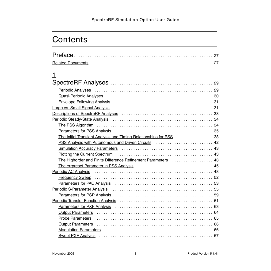
Contents
Preface
Related Documents
SpectreRF Analyses
Periodic Analyses
Quasi-Periodic Analyses
Envelope Following Analysis
Large vs. Small Signal Analysis
Descriptions of SpectreRF Analyses
Periodic Steady-State Analysis
The PSS Algorithm
Parameters for PSS Analysis
The Initial Transient Analysis and Timing Relationships for PSS
PSS Analysis with Autonomous and Driven Circuits
Simulation Accuracy Parameters
Plotting the Current Spectrum
The Highorder and Finite Difference Refinement Parameters
The errpreset Parameter in PSS Analysis
Periodic AC Analysis
Frequency Sweep
Parameters for PAC Analysis
Periodic S-Parameter Analysis
Parameters for PSP Analysis
Periodic Transfer Function Analysis
Parameters for PXF Analysis
Output Parameters
Probe Parameters
Output Parameters
Modulation Parameters
Swept PXF Analysis
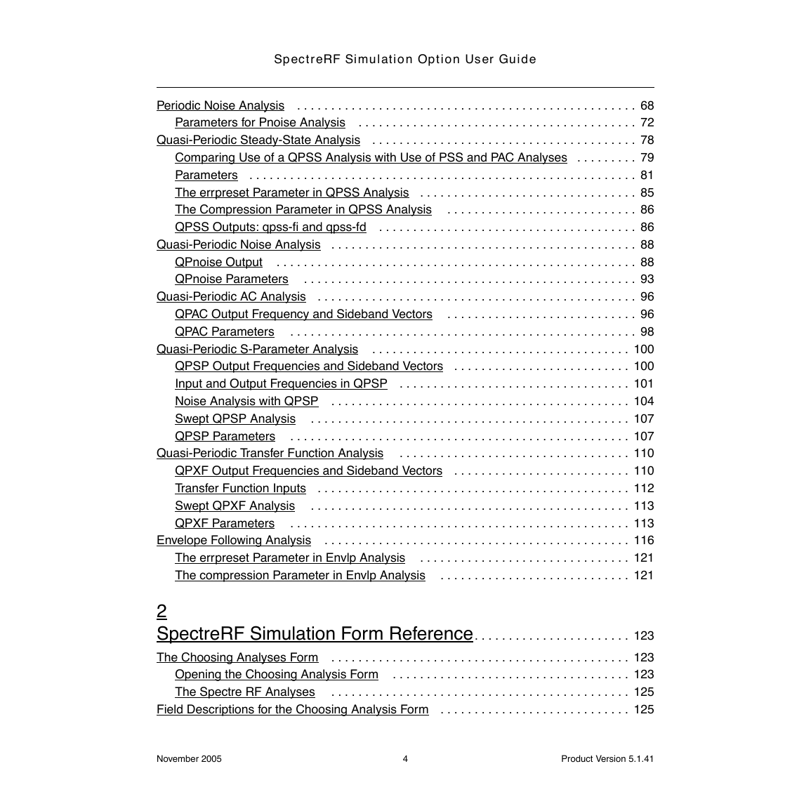
Periodic Noise Analysis
Parameters for Pnoise Analysis
Quasi-Periodic Steady-State Analysis
Comparing Use of a QPSS Analysis with Use of PSS and PAC Analyses
Parameters
The errpreset Parameter in QPSS Analysis
The Compression Parameter in QPSS Analysis
QPSS Outputs: qpss-fi and qpss-fd
Quasi-Periodic Noise Analysis
QPnoise Output
QPnoise Parameters
Quasi-Periodic AC Analysis
QPAC Output Frequency and Sideband Vectors
QPAC Parameters
Quasi-Periodic S-Parameter Analysis
QPSP Output Frequencies and Sideband Vectors
Input and Output Frequencies in QPSP
Noise Analysis with QPSP
Swept QPSP Analysis
QPSP Parameters
Quasi-Periodic Transfer Function Analysis
QPXF Output Frequencies and Sideband Vectors
Transfer Function Inputs
Swept QPXF Analysis
QPXF Parameters
Envelope Following Analysis
The errpreset Parameter in Envlp Analysis
The compression Parameter in Envlp Analysis
SpectreRF Simulation Form Reference
The Choosing Analyses Form
Opening the Choosing Analysis Form
The Spectre RF Analyses
Field Descriptions for the Choosing Analysis Form
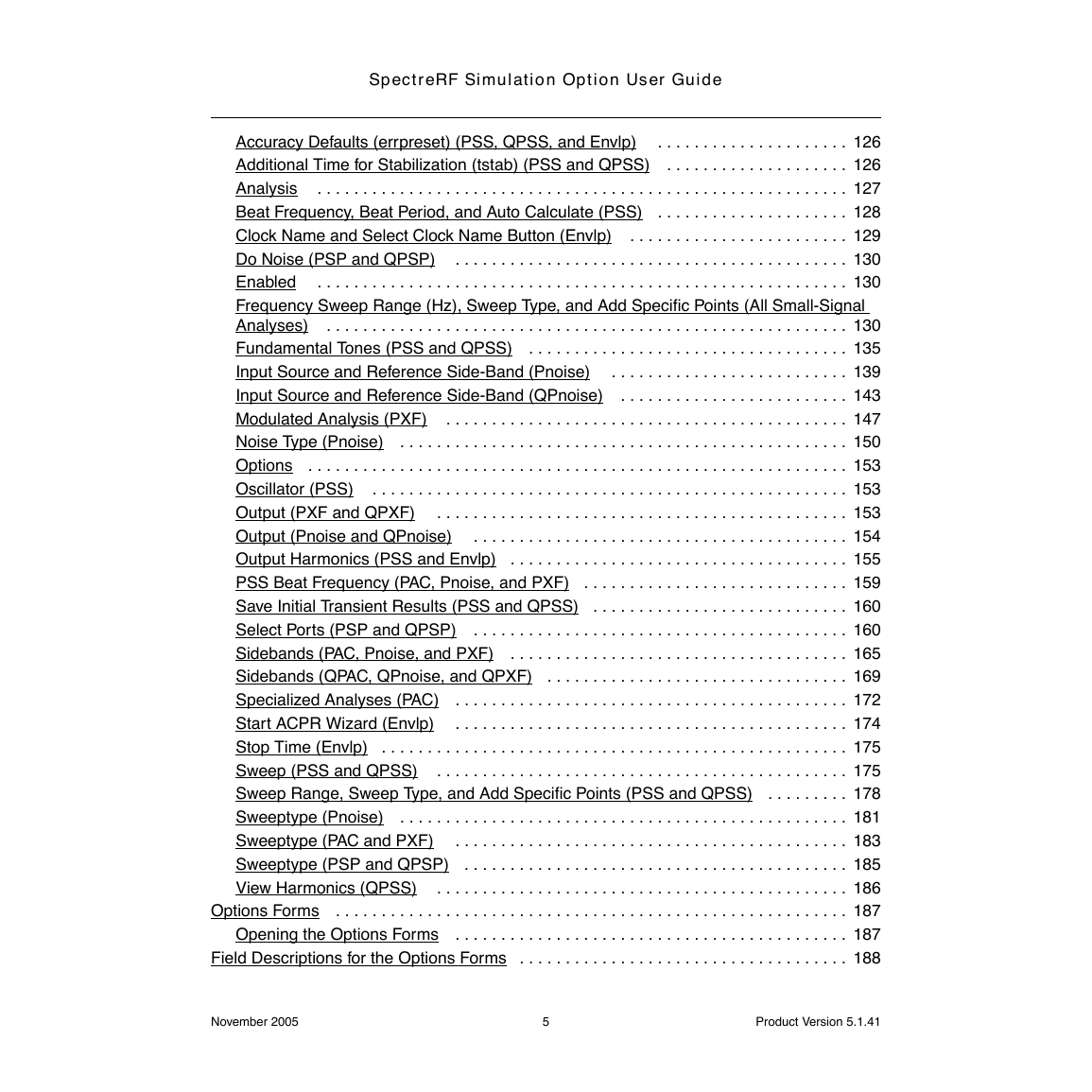
Accuracy Defaults (errpreset) (PSS, QPSS, and Envlp)
Additional Time for Stabilization (tstab) (PSS and QPSS)
Analysis
Beat Frequency, Beat Period, and Auto Calculate (PSS)
Clock Name and Select Clock Name Button (Envlp)
Do Noise (PSP and QPSP)
Enabled
Frequency Sweep Range (Hz), Sweep Type, and Add Specific Points (All Small-Signal Analyses)
Fundamental Tones (PSS and QPSS)
Input Source and Reference Side-Band (Pnoise)
Input Source and Reference Side-Band (QPnoise)
Modulated Analysis (PXF)
Noise Type (Pnoise)
Options
Oscillator (PSS)
Output (PXF and QPXF)
Output (Pnoise and QPnoise)
Output Harmonics (PSS and Envlp)
PSS Beat Frequency (PAC, Pnoise, and PXF)
Save Initial Transient Results (PSS and QPSS)
Select Ports (PSP and QPSP)
Sidebands (PAC, Pnoise, and PXF)
Sidebands (QPAC, QPnoise, and QPXF)
Specialized Analyses (PAC)
Start ACPR Wizard (Envlp)
Stop Time (Envlp)
Sweep (PSS and QPSS)
Sweep Range, Sweep Type, and Add Specific Points (PSS and QPSS)
Sweeptype (Pnoise)
Sweeptype (PAC and PXF)
Sweeptype (PSP and QPSP)
View Harmonics (QPSS)
Options Forms
Opening the Options Forms
Field Descriptions for the Options Forms
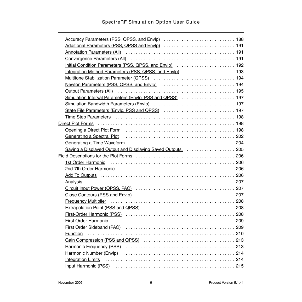
Accuracy Parameters (PSS, QPSS, and Envlp)
Additional Parameters (PSS, QPSS and Envlp)
Annotation Parameters (All)
Convergence Parameters (All)
Initial Condition Parameters (PSS, QPSS, and Envlp)
Integration Method Parameters (PSS, QPSS, and Envlp)
Multitone Stabilization Parameter (QPSS)
Newton Parameters (PSS, QPSS, and Envlp)
Output Parameters (All)
Simulation Interval Parameters (Envlp, PSS and QPSS)
Simulation Bandwidth Parameters (Envlp)
State File Parameters (Envlp, PSS and QPSS)
Time Step Parameters
Direct Plot Forms
Opening a Direct Plot Form
Generating a Spectral Plot
Generating a Time Waveform
Saving a Displayed Output and Displaying Saved Outputs.
Field Descriptions for the Plot Forms
1st Order Harmonic
2nd-7th Order Harmonic
Add To Outputs
Analysis
Circuit Input Power (QPSS, PAC)
Close Contours (PSS and Envlp)
Frequency Multiplier
Extrapolation Point (PSS and QPSS)
First-Order Harmonic (PSS)
First Order Harmonic
First Order Sideband (PAC)
Function
Gain Compression (PSS and QPSS)
Harmonic Frequency (PSS)
Harmonic Number (Envlp)
Integration Limits
Input Harmonic (PSS)
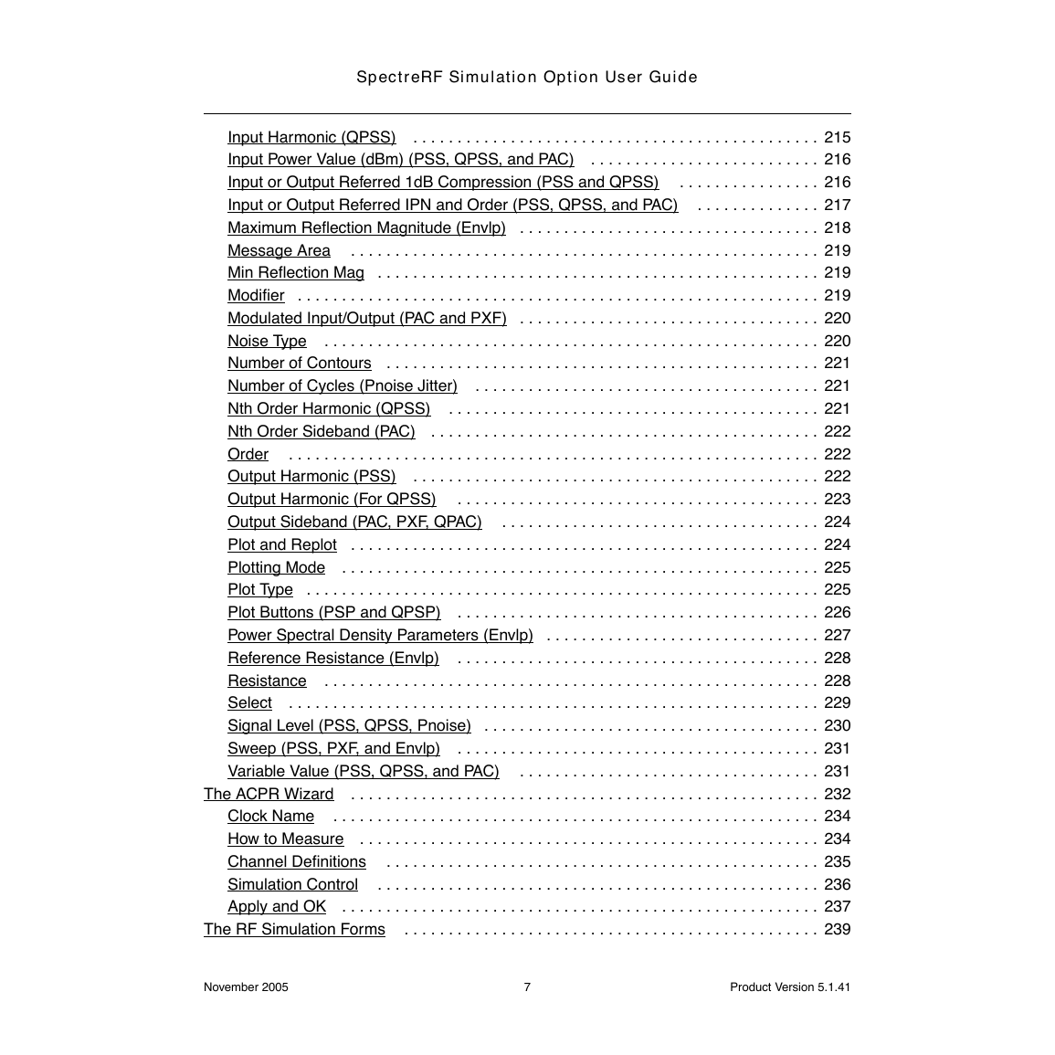
Input Harmonic (QPSS)
Input Power Value (dBm) (PSS, QPSS, and PAC)
Input or Output Referred 1dB Compression (PSS and QPSS)
Input or Output Referred IPN and Order (PSS, QPSS, and PAC)
Maximum Reflection Magnitude (Envlp)
Message Area
Min Reflection Mag
Modifier
Modulated Input/Output (PAC and PXF)
Noise Type
Number of Contours
Number of Cycles (Pnoise Jitter)
Nth Order Harmonic (QPSS)
Nth Order Sideband (PAC)
Order
Output Harmonic (PSS)
Output Harmonic (For QPSS)
Output Sideband (PAC, PXF, QPAC)
Plot and Replot
Plotting Mode
Plot Type
Plot Buttons (PSP and QPSP)
Power Spectral Density Parameters (Envlp)
Reference Resistance (Envlp)
Resistance
Select
Signal Level (PSS, QPSS, Pnoise)
Sweep (PSS, PXF, and Envlp)
Variable Value (PSS, QPSS, and PAC)
The ACPR Wizard
Clock Name
How to Measure
Channel Definitions
Simulation Control
Apply and OK
The RF Simulation Forms
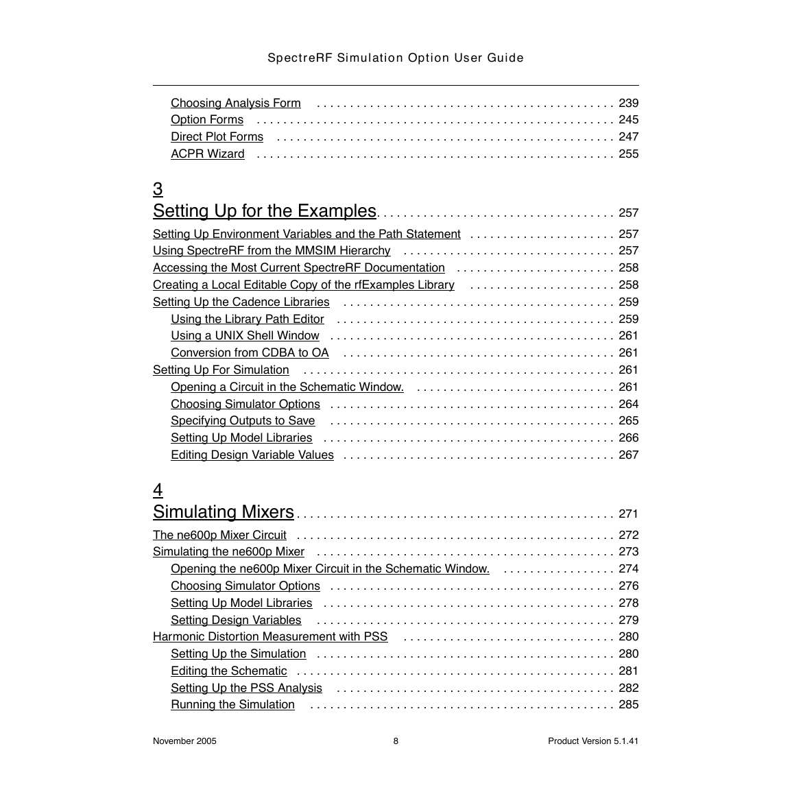
Choosing Analysis Form
Option Forms
Direct Plot Forms
ACPR Wizard
Setting Up for the Examples
Setting Up Environment Variables and the Path Statement
Using SpectreRF from the MMSIM Hierarchy
Accessing the Most Current SpectreRF Documentation
Creating a Local Editable Copy of the rfExamples Library
Setting Up the Cadence Libraries
Using the Library Path Editor
Using a UNIX Shell Window
Conversion from CDBA to OA
Setting Up For Simulation
Opening a Circuit in the Schematic Window.
Choosing Simulator Options
Specifying Outputs to Save
Setting Up Model Libraries
Editing Design Variable Values
Simulating Mixers
The ne600p Mixer Circuit
Simulating the ne600p Mixer
Opening the ne600p Mixer Circuit in the Schematic Window.
Choosing Simulator Options
Setting Up Model Libraries
Setting Design Variables
Harmonic Distortion Measurement with PSS
Setting Up the Simulation
Editing the Schematic
Setting Up the PSS Analysis
Running the Simulation
Plotting and Calculating Harmonic Distortion
Noise Figure Measurement with PSS and Pnoise
Setting Up the Simulation
Editing the Schematic
Setting up the PSS and Pnoise Analyses
Running the Simulation
Plotting the Noise Figure
Noise Figure Measurement and Periodic S-Parameter Plots with PSS and PSP
Setting Up the Simulation
Editing the Schematic
Setting up the PSS and PSP Analyses
Running the Simulation
Plotting the Noise Figure
Plotting Periodic S-Parameters
Conversion Gain Measurement with PSS and PXF
Setting Up the Simulation
Editing the Schematic
Setting Up the PSS and PXF Analyses
Running the Simulation
Plotting the Conversion Gain
Plotting the Power Supply Rejection
Calculating the 1 dB Compression Point with Swept PSS
Setting Up the Simulation
Editing the Schematic
Setting Up the Swept PSS Analysis
Running the Simulation
Plotting the 1 dB Compression Point
Third-Order Intercept Measurement with Swept PSS and PAC
Setting Up the Simulation
Editing the Schematic
Setting Up the PSS and PAC Analyses
Running the Simulation
Plotting the IP3 Curve
Intermodulation Distortion Measurement with QPSS
Setting Up the Simulation
Editing the Schematic
Setting Up the QPSS Analysis
Selecting Simulation Outputs
Running the Simulation
Plotting the Voltage and Power
Noise Figure with QPSS and QPnoise
Setting Up the Simulation
Editing the Schematic
Setting Up the QPSS and QPnoise Analyses
Selecting Simulation Outputs
Running the Simulation
Plotting the Noise Figure
Plotting the Output Noise
Simulating Oscillators
Autonomous PSS Analysis
Phases of Autonomous PSS Analysis
Phase Noise and Oscillators
Starting and Stabilizing the Oscillator
The tline3oscRF Oscillator Circuit
Simulating tline3oscRF Oscillator Circuit with MIC
Opening the tline3oscRF Circuit in the Schematic Window
Choosing Simulator Options
Setting Up Model Libraries
Periodic Steady State and Phase Noise with PSS and Pnoise
Setting Up the Simulation
Setting Up the MIC-PSS Analysis
Setting Up the Pnoise Analysis
Running the Simulation
Plotting the Fundamental Frequency
Plotting the Periodic Steady State Solution
Plotting the Phase Noise
Checking the Simulation Log File for MIC-PSS Information
The oscDiff Circuit: A Balanced, Tunable Differential Oscillator
Simulating the oscDiff Circuit
Opening the oscDiff Circuit in the Simulation Window
Choosing Simulator Options
Setting Up Model Libraries
Fundamental Frequency, Output Noise, and Phase Noise with PSS and Pnoise
Setting Up the Simulation
Editing Design Variables
Setting Up the PSS Analysis
Setting Up the Pnoise Analysis
Running the Simulation
Plotting the Fundamental Frequency
Plotting the Output Noise and Phase Noise
The Van der Pol Circuit: Measuring AM and PM Noise Separation
Simulating the vdp_osc Circuit
Opening the vdp_osc Circuit
Editing Properties for the Inductor
Opening the Simulation Window
Measuring AM and PM Conversion with PSS and Pnoise
Setting Up the Simulation
Setting Up the PSS Analysis
Setting Up the Pnoise Analysis
Running the Simulation
Plotting Modulated Pnoise with the dBV Modifier
Plotting Modulated Pnoise with the dBc Modifier
Measuring Jitter with PSS and Pnoise Jitter Analyses
Opening the oscDiff Circuit
Opening the Simulation Window
Editing Design Variables
Setting Up the Simulation
Specifying Outputs to Save
Setting Up the PSS Analysis
Setting Up the Pnoise Analysis
Running the Simulation
Measuring Jitter
Troubleshooting for Oscillator Circuits
Simulating Low-Noise Amplifiers
Analyses and Measurement Examples in this Chapter
Simulating the lnaSimple Example
Opening the lnaSimple Circuit in the Schematic Window
Choosing Simulator Options
Setting Up Model Libraries
Calculating Voltage Gain with PSS
Setting Up the Simulation
Editing the Schematic
Setting Up the PSS Analysis
Running the Simulation
Plotting Voltage Gain
Calculating Output Voltage Distribution with PSS
Setting Up the Simulation
Editing the Schematic
Setting up the PSS Analysis
Running the Simulation
Plotting the Output Voltage Distribution
S-Parameter Analysis for Low Noise Amplifiers
Setting Up the Simulation
Editing the Schematic
Setting up the S-Parameter Analysis
Running the Simulation
Plotting S-Parameters
Plotting the Voltage Standing Wave Ratio
Linear Two-Port Noise Analysis with S-Parameters
Setting Up the Simulation
Editing the Schematic
Setting up the S-Parameter Analysis
Running the Simulation
Plotting the Noise Figure and Minimum Noise Figure
Plotting the Equivalent Noise Resistance
Plotting Load and Source Stability Circles
Plotting the Noise Circles
Noise Calculations with PSS and Pnoise
Setting Up the Simulation
Editing the Schematic
Setting up the PSS and Pnoise Analyses
Running the Simulation
Plotting the Noise Calculations
Plotting the 1dB Compression Point
Setting Up the Simulation
Editing the Schematic
Setting up the PSS Analysis
Running the Simulation
Plotting the 1dB Compression Point
Calculating the Third-Order Intercept Point with Swept PSS
Setting Up the Simulation
Editing the Schematic
Setting up the Swept PSS Analysis
Running the Simulation
Plotting the Third-Order Intercept Point
Calculating Conversion Gain and Power Supply Rejection with PSS and PXF
Setting Up the Simulation
Editing the Schematic
Setting up the PSS and PXF Analyses
Running the Simulation
Plotting Conversion Gain and Power Supply Rejection
Modeling Transmission Lines
The Transmission Line Models: tline3, mline, and mtline
The tline3 Model
The mline Model
The mtline Model
LMG Use Models
Modeling Transmission Lines Using the LMG GUI
Modeling Transmission Lines Without Using the Visual Interface
Default Values and the initlmg File
Tline3 Transmission Line Modeling Examples
Creating a tline3 Macromodel in the LMG GUI
Using an Existing tline3 Macromodel in the Schematic Flow
Resolving A Possible Error Message for a tline3 Model File
Creating a tline3 Macromodel in the Schematic Flow
Mline Transmission Line Modeling Examples
Creating an mline Transmission Line Model Starting LMG From UNIX
Using an mline Macromodel in the Schematic Flow
Resolving a Possible Error Message for an mline Model File
Creating an mline Transmission Line in the Schematic Flow
Using LMG and mtline Together in the Analog Design Environment
Coplanar Waveguide Modeling and Analysis
Using LMG to Obtain Subcircuit Macromodel and LRCG Files
General Theory of Coplanar Waveguide Analysis
Simulating Coplanar Waveguides with the Generated LRCG File
Verifying Input Signal Corruption by Microstrip Line Reflection
Simulating Coplanar Waveguides with the Generated Subcircuit Macromodel File
Internal Techniques in LMG and Model Accuracy
The LMG GUI Reference
Menus
Display Section
Data Entry Section
Function Buttons
Modeling RF IC Packages
The Four PKG Building Blocks
Package Physical Geometry Modeling
EM Solvers and Mesh Making
Macromodel Generation
PKG Setup Requirements
License Checking
Executables
PKG GUI Files
Initialization Files
Running pkg
The PKG RF IC Package Modeler Window
Menu Buttons
Function Buttons
Package Dimension Setup
QFP Packages
Data Entries for QFP Packages
SOIC Packages
Data Entries for SOIC Packages
DIP Packages
Data Entries for DIP Packages
Die Attach Setup
Data Entries for SOIC Packages
Internal Lead Frame Setup
Menu Buttons
Function Buttons
Data Entries for the Internal Lead Frame Setup
More about Using Symmetry
Lead Frame File Format
Bond Wire Setup
Menu Buttons
Function Buttons
Data Entries for the Bond Wire Setup
Bond Wire Configurations
Bond Wire File Format
Save the Current Setting
Parameter Extraction
Capacitance Calculation
Inductance Calculation
Function Buttons for Parameter Extraction
Macromodel Generation
Data Entries and Buttons for Macromodel Generation
Die Attach Terminal
Macromodel Schematic
High Frequency Resonance Damping for the Spectre Simulator
Accuracy Analysis
Simulation of Package Models in the Analog Circuit Design Environment
Example of Package Modeling With a Mixer Using PKG
Creating and Using Receiver K-Models
Procedures for Simulating k_mod_extraction_example
Analysis Setup
Setting Up the Analyses
Running the Simulation
Checking the Simulation Results
Creating the K-Model
More About the K-Model
K-model data files
Creating and Using Transmitter J-Models
Procedures for Simulating j_mod_extraction_example
Analysis Setup
Running the Simulation
Creating the J-Model
Using the J-model in a Circuit
More About the J-model
Modeling Transmitters
Envelope Following Analysis
Opening the EF_example Circuit in the Schematic Window
Opening the Simulation Window
Setting Up the Model Libraries
PORT0 and PORT1 in the Schematic Window
Setting Up an Envelope Following Analysis
Looking at the Envelope Following Results
Following the Baseband Signal Changes Through an Ideal Circuit
Following the Baseband Signal Changes Through a Non-Ideal Circuit
Plotting the Complete Baseband Signal
Plotting the Baseband Trajectory
Measuring ACPR and PSD
The ACPR Wizard
Measuring ACPR
Setting Up the ACPR Wizard and the envlp Analysis
Estimating PSD From the Direct Plot Form
Reference Information for ACPR and PSD Calculations
Measuring Load-Pull Contours and Load Reflection Coefficients
Creating and Setting Up the Modified Circuit
Setting Up and Running the PSS and Parametric Analyses
Displaying Load Contours
Adding the Reflection Contours to the Plot
Moving to Differential Mode
Using S-Parameter Input Files
Setting Up the EF_example Schematic for the First Simulation
Adding Components to the Schematic
Setting Up the s.param.first Schematic
Running the SP Simulation
The S�Parameter File
Setting Up and Running the Second sp Simulation
Using an S-Parameter Input File with a SpectreRF Envlp Analysis
Measuring AM and PM Conversion with Modulated PAC and PXF Analyses
The Modulated Analysis Settings
Creating the EF_AMP Circuit
Setting Up the EF_AMP Circuit
Opening the Simulation Window for the EF_AMP Circuit
Edit the Variable Values
Setting up the Model Libraries for the EF_AMP Circuit
Selecting Outputs To Save
Setting Up and Running the PSS, PAC Modulated and PXF Modulated Analyses
Running the Simulations
Plotting and Calculating PAC Modulated Results
Plotting and Calculating PXF Modulated Results
Measuring Jitter with PSS and Pnoise Analyses
Setting Up the EF_AMP Circuit
Open the EF_AMP Schematic
Open the Simulation Window for the EF_AMP Circuit
Setting Up and Running the PSS and Pnoise Analyses
Running the Simulations
Plotting the Jitter Measurement
Modeling Spiral Inductors, Bonding Pads, and Transformers
Modeling Spiral Inductors
Process File Preparation
Spiral Inductor Simulation in the Schematic Flow
Spiral Inductor Modeling under the RF Sub-Menu
Equivalent Circuit Models
Rectangular Spiral Inductor Example
Modeling Bonding Pads
Process Files
Parameter Sets
Modeling Issues
LNA Example with Bonding Pads
References for the Bondpad Section
Modeling Planar Transformers
Process File
Symbols and CDF Parameters for Planar Transformers
Planar Transformer Modeling Under the RF Sub-Menu
Equivalent Circuit Models
Methods for Top-Down RF System Design
Methods for Top Down RF System Design
Top-Down Design of RF Systems
Use Model for Top Down Design
Baseband Modeling
Example Comparing Baseband and Passband Models
Library Overview
Warnings You Can Ignore
Use Model and Design Example
Opening a New Schematic Window
Opening the Analog Environment
Constructing the Baseband Model for the Receiver
Setting Variable Values for the Receiver Schematic
Setting Up and Running a Transient Analysis
Examining the Results: Eye Diagram, Histogram, and Scatter Plot
The Various Instrumentation Blocks
Measuring RMS EVM
Computing Minimized RMS Noise Using the Optimizer
Summarizing the Design Procedure
Creating a Passband View of the Architectural Model
Comparing Baseband and Passband Models
Relationship Between Baseband and Passband Noise
Intro to Analysis
Prep Steps for Analyses
Oscillator Noise Analysis
Phase Noise Primer
Models for Phase Noise
Linear Time-Invariant (LTI) Models
Linear Time-Varying (LTV) Models
Amplitude Noise and Phase Noise in the Linear Model
Details of the SpectreRF Calculation
Calculating Phase Noise
Setting Simulator Options
Tips for Getting a PSS Analysis to Converge
How to Tell if the Answer Is Correct
Troubleshooting Phase Noise Calculations
Known Limitations of the Simulator
What Can Go Wrong
Phase Noise Error Messages
The tstab Parameter
Frequently Asked Questions
Further Reading
References
Using PSS Analysis Effectively
General Convergence Aids
Adjusting the steadyratio and tstab Parameters
Additional Convergence Aids
Convergence Aids for Oscillators
Running PSS Analysis Hierarchically
Using the psin Component
Independent Resistive Source (psin)
Capabilities of the psin Component
Terminating the psin
Parameter Types for the psin Component
Name Parameters
psin Instance Parameter
General Waveform Parameters
Sinusoidal Waveform Parameters
Amplitude Modulation Parameters
FM Modulation Parameters
Noise Parameters
Port Parameters
Temperature Effect Parameters
Small-Signal Parameters
Additional Notes
The RF Library
The Contents of the rfLib
Elements for Transistor-Level RF Circuit Design: Original_RFAHDL_lib Category
Elements for Top-Down System-Level RF Design: the top_dwnBB and top_dwnPB Categories
Elements for Both Transistor-Level and System-Level RF Design: the measurement and testbenches Ca...
Elements for Bottom Up Transmitter Design: the bot_upBB Category
Models for Transistor-Level RF Circuit Design
Original_RFAHDL_lib Elements
Balun
Butterworth and Chebyshev Filters
Low-Noise Amplifier (lna)
Mixer
Oscillator (osc)
Power Amplifier (pa)
Quadrature Signal Generator (quadrature)
Phase Shifter (shifter)
Measurement Elements
CDMA Signal Source (CDMA_reverse_xmit)
GSM Signal Source (GSM_xmtr)
Pi/4-DQPSK Signal Source (pi_over4_dqpsk)
Eye-Diagram Generator (eye_diagram_generator)
Modifying the Baseband Signal Generators Using the Modelwriter
Testbenches Elements
Uncategorized Elements
Bottom-Up Design Elements
Models for Top-Down RF System Design
Baseband and Passband Models
Assumptions About Behavioral Models
Inputs and Outputs for Baseband Models
Some Common Model Parameters
Library Description
Notes on models involving frequency translation
Top Down Baseband and Passband Models: top_dwnBB and top_dwn PB
Power Amplifier Models (PA_BB and PA_PB)
Low Noise Amplifier Baseband Models (LNA_BB and LNA_PB)
IQ Modulator Models (IQ_mod_BB and IQ_mod_PB)
IQ Demodulator (IQ_demod_BB and IQ_demodulator)
RF-to-IFand IF-to-RF Mixers (up_cnvrt, dwn_cnvrt and MIXER_PB)
Passive Devices (res_BB, cap_BB and ind_BB)
Linear Time Invariant Filters
BB_Loss
Phase Shifter Splitter
Phase Shifter Combiner
Comparison of Baseband and Passband Models
Measurement Blocks
Ideal Transformer
Rectangular-to-Polar Transformation
Polar-to-Rectangular Transformation
Instrumentation and Terminating Blocks
Baseband Drive Signals
BB_driver
References
Plotting Spectre S-Parameter Simulation Data
Network Parameters
Equations for Network Parameters
Two-Port Scalar Quantities
Equations for Two-Port Scalar Quantities
Two-Port Gain Quantities
Equations for Two-Port Gain Calculations
Two-Port Network Circles
Equations for Two-Port Network Circle
Equation for VSWR (Voltage Standing Wave Ratio)
Equation for ZM (Input Impedance)
Equation for GD (group delay)
Using QPSS Analysis Effectively
When Should You Use QPSS Analysis
Essentials of the MFT Method
QPSS and PSS Analyses Compared
QPSS and PSS/PAC Analyses Compared
QPSS Analysis Parameters
Application Examples
Switched Capacitor Filter Example
High-Performance Receiver Example
Running a QPSS Analysis
Picking the Large Fundamental
Setting Up Sources
Sweeping a QPSS Analysis
Convergence Aids
Memory Management
Dealing with Sub-harmonics
Understanding the Narration from the QPSS Analysis
References
Introduction to the PLL library
Models in the PLL library
Introduction
Phase-Domain Model of a Simple PLL
Example 1: Dynamic Test for Capture Range and Lock Range
Example 2: Loop Gain Measurement
Example 3: PM Input
Modeling a PFD-Based PLL
VCO
Frequency Divider
Charge Pump
Loop Filter
State-Space Averaged PFD (Phase-Domain Phase-Frequency Detector Model)
Lock Indicator
Example 5: Comparison With a Voltage-Domain Model
How the PFD Model Works
How the PDF/CP Pump Works
References
Using the Port Component
The Independent Resistive Source or Port Component
Capabilities of the Port Component
Terminating the Port Component
Port Component Parameters
General Port Parameters
General Waveform Parameters
DC Waveform Parameters
Pulse Waveform Parameters
PWL Waveform Parameters
Sinusoidal Waveform Parameters
Modulation Parameters
Display Second Sinusoid Parameters
Exponential Waveform Parameters
Noise Parameters
Small-Signal Parameters
Temperature Parameters
How the Temperature Parameters Affect the Voltage Level
Active Parameters in Specific Analyses
Analyzing Time-Varying Noise
Characterizing Time-Domain Noise
Calculating Time Domain Noise
Calculating Noise Correlation Coefficients
Cyclostationary Noise Example
Reference Information on Time-Varying Noise
Thermal Noise
Linear Systems and Noise
Time-Varying Systems and the Autocorrelation Function
Time-Varying Systems and Frequency Correlations
Time-Varying Noise Power and Sampled Systems
Summary
Using Tabulated S-parameters
Using the nport Components
Controlling Model Accuracy
Using relerr and abserr
Using the ratorder Parameter
Troubleshooting
Assessing the Quality of the Rational Interpolation
Model Reuse
The S-Parameter File Format Translator (SPTR)
References
Measuring AM, PM and FM Conversion
Derivation
Positive Frequencies
FM Modulation
Simulation
Results
Conclusion
References
Using PSP and Pnoise Analyses
Overview
Periodic S-parameters
Linear Time-Invariant S-Parameters
Frequency Translating S-Parameters
Upper and Lower Sidebands
PSP Analysis Example
Noise and Noise Parameters
Calculating Noise in Linear Time-Invariant (DC Bias) Circuits
Calculating Noise in Time-Varying (Periodic Bias) Circuits
The maxsideband Parameter
Noise Correlation Matrices and Equivalent Noise Sources
Noise Figure
Performing Noise Figure Computations
Noise Figure From Noise and SP Analyses
Pnoise (SSB) Noise Figure
DSB Noise Figure
IEEE Noise Figure
Noise Computation Example
Input Referred Noise
Using Input Referred Noise
How IRN is Calculated
Relation to Gain
Referring Noise to Ports
Gain Calculations
Definitions of Gain
Gain Calculations in Pnoise
Phase Noise
Frequently Asked Questions
Known Problems and Limitations
Dubious AC-Noise Analysis Features
Gain in Pnoise and PSP Analyses Inconsistent
Harmonics and Sidebands in PSP, PAC, PXF, and Pnoise Analyses
Index


 2023年江西萍乡中考道德与法治真题及答案.doc
 2012年重庆南川中考生物真题及答案.doc
 2013年江西师范大学地理学综合及文艺理论基础考研真题.doc
 2020年四川甘孜小升初语文真题及答案I卷.doc
 2020年注册岩土工程师专业基础考试真题及答案.doc
 2023-2024学年福建省厦门市九年级上学期数学月考试题及答案.doc
 2021-2022学年辽宁省沈阳市大东区九年级上学期语文期末试题及答案.doc
 2022-2023学年北京东城区初三第一学期物理期末试卷及答案.doc
 2018上半年江西教师资格初中地理学科知识与教学能力真题及答案.doc
 2012年河北国家公务员申论考试真题及答案-省级.doc
 2020-2021学年江苏省扬州市江都区邵樊片九年级上学期数学第一次质量检测试题及答案.doc
 2022下半年黑龙江教师资格证中学综合素质真题及答案.doc