应用笔记
APPLICATION NOTE
APPLICATION NOTE
U-100A
U-100A
U-100A
UC3842/3/4/5 PROVIDES LOW-COST
UC3842/3/4/5 PROVIDES LOW-COST
电流模式控制
UC3842/3/4/5提供了低成本的
CURRENT-MODE CONTROL
CURRENT-MODE CONTROL
INTRODUCTION
INTRODUCTION
引言
The fundamental challenge of power supply design is to
The fundamental challenge of power supply design is to
simultaneously realize two conflicting objectives: good
simultaneously realize two conflicting objectives: good
电源设计的主要难题是需要同时实现两个相互矛盾的目标,
electrical performance and low cost. The
electrical performance and low cost. The
即:上佳的电性能和低成本。UC3842/3/4/5是一款集成脉宽
designed
is an integrated pulse width modulator
designed
is an integrated pulse width modulator
调制器 (PWM),它在设计时兼顾了上述的两个目标。该IC
provides de-
with both these objectives in mind. This
provides de-
with both these objectives in mind. This
为设计师提供了一款廉价的控制器,他们借助该控制器能够
signers an inexpensive controller with which they can ob-
signers an inexpensive controller with which they can ob-
获得电流模式操作的所有性能优势。此外,UC3842系列还
tain all the performance advantages of current mode op-
tain all the performance advantages of current mode op-
eration. In addition, the UC3842 series is optimized for ef-
专为隔离式转换器和DC-DC稳压器的高效电源排序以及功率
eration. In addition, the UC3842 series is optimized for ef-
ficient power sequencing of off-line converters, DC to DC
ficient power sequencing of off-line converters, DC to DC
MOSFET或晶体管的驱动进行了优化。
regulators and for driving power MOSFETs or transistors.
regulators and for driving power MOSFETs or transistors.
This application note provides a functional description of
本应用笔记提供了UC3842系列的功能描述,并突出介绍了其
This application note provides a functional description of
the UC3842 family and highlights the features of each in-
the UC3842 family and highlights the features of each in-
每个成员 (UC3842、UC3843、UC3844和UC3845) 的特点。
dividual member, the UC3842, UC3843, UC3844 and
dividual member, the UC3842, UC3843, UC3844 and
文章通篇以型号为UC3842的器件为参考,不过,除非特别注
UC3845 Throughout the text, the UC3842 part number
UC3845 Throughout the text, the UC3842 part number
明,否则一般化的电路和性能特征将适用于UC3842系列的所
will be referenced, however the generalized circuits and
will be referenced, however the generalized circuits and
有成员。本文评述了电流模式控制及其好处,并提及了避免
performance characteristics apply to each member of the
performance characteristics apply to each member of the
常见易犯错误的方法。最后的章节给出了运用UC3842控制器
UC3842 series unless otherwise noted. A review of cur-
UC3842 series unless otherwise noted. A review of cur-
rent mode control and its benefits is included and meth-
的电源设计方案。
rent mode control and its benefits is included and meth-
ods of avoiding common pitfalls are mentioned. The final
ods of avoiding common pitfalls are mentioned. The final
section presents designs of power supplies utilizing
section presents designs of power supplies utilizing
UC3842 control.
UC3842 control.
CURRENT-MODE CONTROL
CURRENT-MODE CONTROL
电流模式控制
Figure 1 shows the two-loop current-mode control system
Figure 1 shows the two-loop current-mode control system
in a typical buck regulator application. A clock signal initi-
in a typical buck regulator application. A clock signal initi-
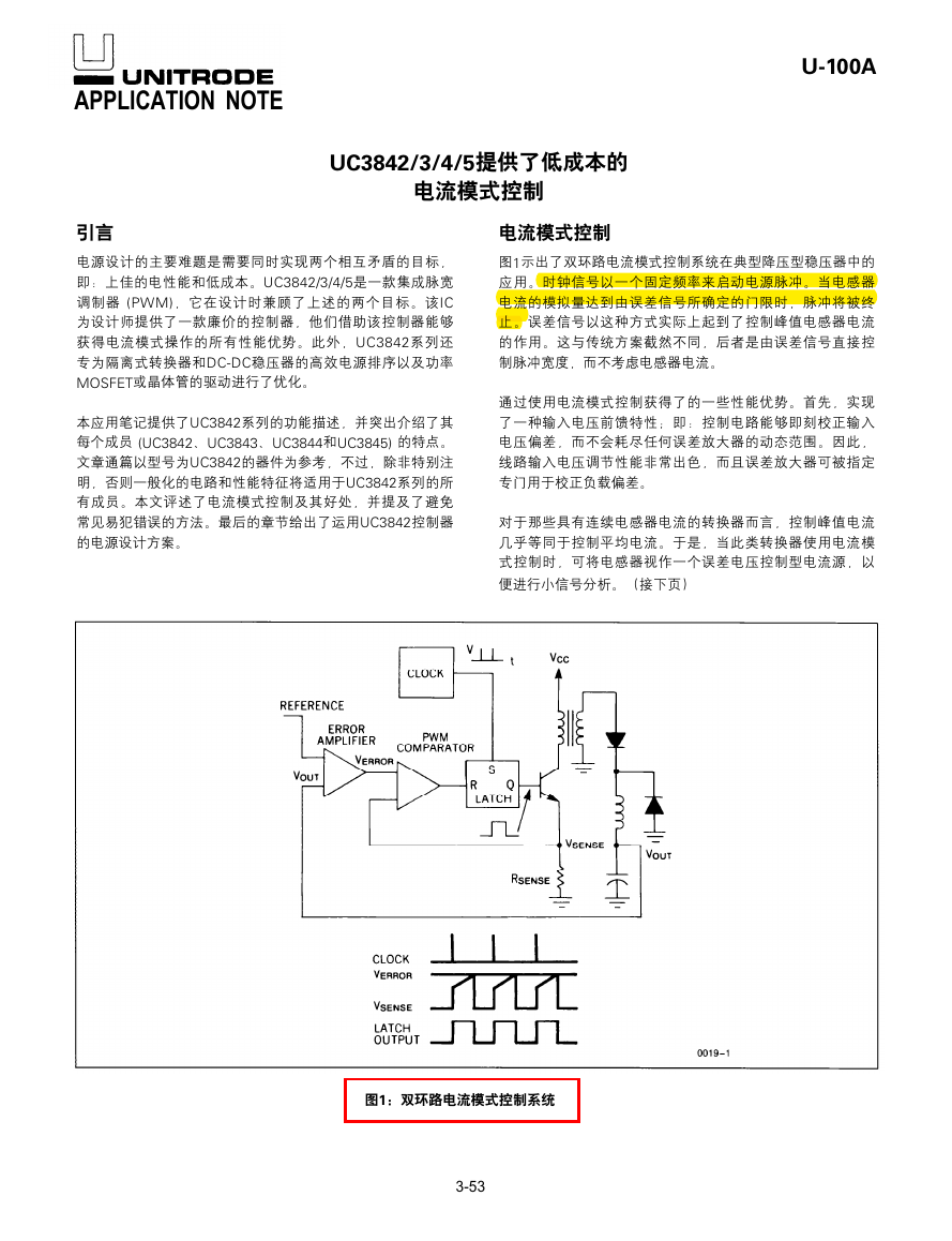
图1示出了双环路电流模式控制系统在典型降压型稳压器中的
ates power pulses at a fixed frequency. The termination of
ates power pulses at a fixed frequency. The termination of
应用。时钟信号以一个固定频率来启动电源脉冲。当电感器
each pulse occurs when an analog of the inductor current
each pulse occurs when an analog of the inductor current
电流的模拟量达到由误差信号所确定的门限时,脉冲将被终
reaches a threshold established by the error signal. In this
reaches a threshold established by the error signal. In this
止。误差信号以这种方式实际上起到了控制峰值电感器电流
way the error signal actually controls peak inductor cur-
way the error signal actually controls peak inductor cur-
的作用。这与传统方案截然不同,后者是由误差信号直接控
rent. This contrasts with conventional schemes in which
rent. This contrasts with conventional schemes in which
the error signal directly controls pulse width without regard
制脉冲宽度,而不考虑电感器电流。
the error signal directly controls pulse width without regard
to inductor current.
to inductor current.
通过使用电流模式控制获得了的一些性能优势。首先,实现
Several performance advantages result from the use of
Several performance advantages result from the use of
current-mode control. First, an input voltage feed-forward
了一种输入电压前馈特性;即:控制电路能够即刻校正输入
current-mode control. First, an input voltage feed-forward
characteristic is achieved; i.e., the control circuit instanta-
characteristic is achieved; i.e., the control circuit instanta-
电压偏差,而不会耗尽任何误差放大器的动态范围。因此,
neously corrects for input voltage variations without using
neously corrects for input voltage variations without using
线路输入电压调节性能非常出色,而且误差放大器可被指定
up any of the error amplifier’s dynamic range. Therefore,
up any of the error amplifier’s dynamic range. Therefore,
专门用于校正负载偏差。
line regulation is excellent and the error amplifier can be
line regulation is excellent and the error amplifier can be
dedicated to correcting for load variations exclusively.
dedicated to correcting for load variations exclusively.
对于那些具有连续电感器电流的转换器而言,控制峰值电流
For converters in which inductor current is continuous,
For converters in which inductor current is continuous,
几乎等同于控制平均电流。于是,当此类转换器使用电流模
controlling peak current is nearly equivalent to controlling
controlling peak current is nearly equivalent to controlling
式控制时,可将电感器视作一个误差电压控制型电流源,以
average current. Therefore, when such converters employ
average current. Therefore, when such converters employ
便进行小信号分析。(接下页)
current-mode control, the inductor can be treated as an
current-mode control, the inductor can be treated as an
Figure 1. Two-Loop Current-Mode Control System
Figure 1. Two-Loop Current-Mode Control System
图1:双环路电流模式控制系统
3-53
3-53
�
APPLICATION NOTE
应用笔记
error-voltage-controlled-current-source for the purposes of
small-signal analysis. This is illustrated by Figure 2. The
two-pole control-to-output frequency response of these
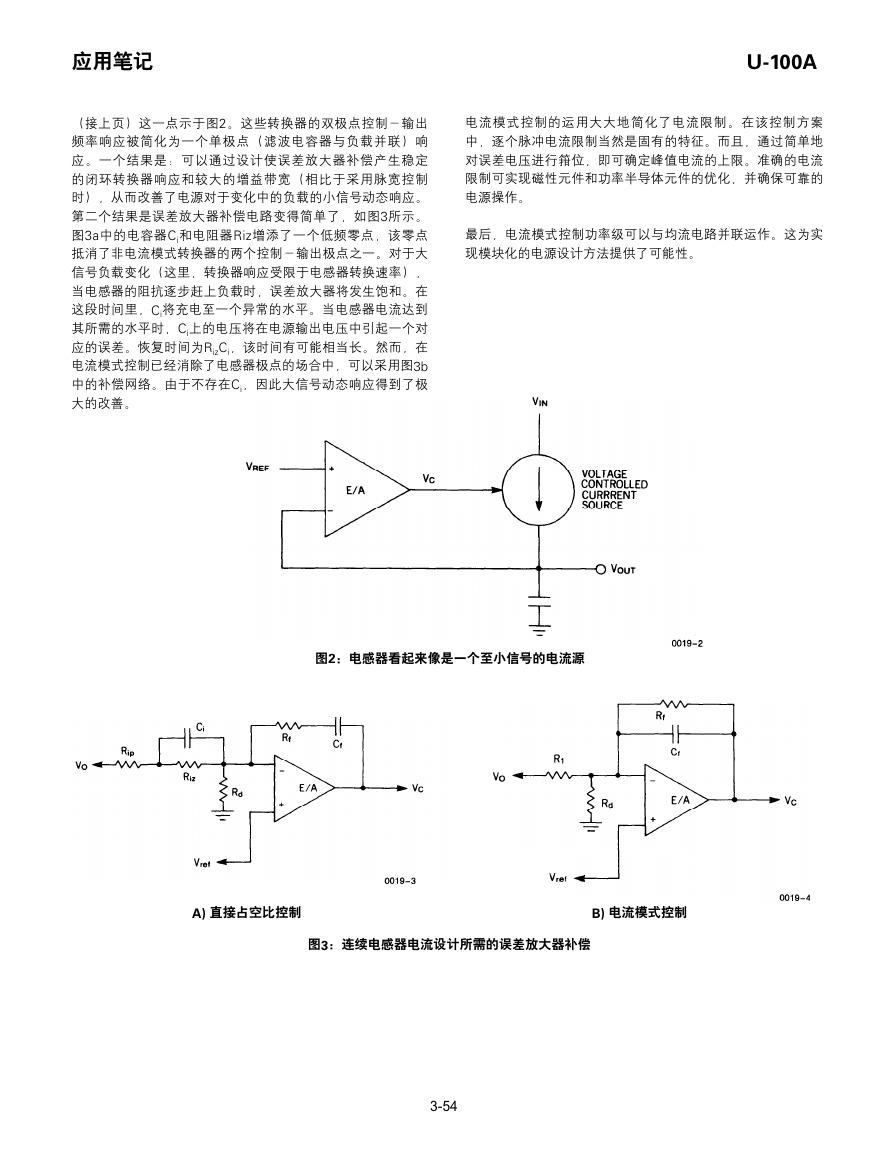
(接上页)这一点示于图2。这些转换器的双极点控制-输出
converters is reduced to a single-pole (filter capacitor in
频率响应被简化为一个单极点(滤波电容器与负载并联)响
parallel with load) response. One result is that the error
应。一个结果是:可以通过设计使误差放大器补偿产生稳定
amplifier compensation can be designed to yield a stable
的闭环转换器响应和较大的增益带宽(相比于采用脉宽控制
closed-loop converter response with greater gainband-
时),从而改善了电源对于变化中的负载的小信号动态响应。
width than would be possible with pulse-width control, giv-
ing the supply improved small-signal dynamic response to
第二个结果是误差放大器补偿电路变得简单了,如图3所示。
changing loads. A second result is that the error amplifier
图3a中的电容器Ci和电阻器Riz增添了一个低频零点,该零点
compensation circuit becomes simpler, as illustrated in Fig-
抵消了非电流模式转换器的两个控制-输出极点之一。对于大
ure 3. Capacitor
in Figure 3a add a low
信号负载变化(这里,转换器响应受限于电感器转换速率),
frequency zero which cancels one of the two control-to-.
当电感器的阻抗逐步赶上负载时,误差放大器将发生饱和。在
output poles of non-current-mode converters. For large-
这段时间里,Ci将充电至一个异常的水平。当电感器电流达到
signal load changes, in which converter response is limit-
其所需的水平时,Ci上的电压将在电源输出电压中引起一个对
ed by inductor slew rate, the error amplifier will saturate
while the inductor is catching up with the load. During this
应的误差。恢复时间为RizCi,该时间有可能相当长。然而,在
will charge to an abnormal level. When the induc-
time,
电流模式控制已经消除了电感器极点的场合中,可以采用图3b
tor current reaches its required level, the voltage on
中的补偿网络。由于不存在Ci,因此大信号动态响应得到了极
大的改善。
and resistor
U-100A
U-100A
U-100A
causes a corresponding error in supply output voltage.
The recovery time is
which may be quite long. How-
can be used
ever, the compensation network of Figure
电流模式控制的运用大大地简化了电流限制。在该控制方案
where current-mode control has eliminated the inductor
中,逐个脉冲电流限制当然是固有的特征。而且,通过简单地
pole. Large-signal dynamic response is then greatly im-
对误差电压进行箝位,即可确定峰值电流的上限。准确的电流
proved due to the absence of
限制可实现磁性元件和功率半导体元件的优化,并确保可靠的
Current limiting is greatly simplified with current-mode con-
电源操作。
trol. Pulse-by-pulse limiting is, of course, inherent in the
control scheme. Furthermore, an upper limit on the peak
最后,电流模式控制功率级可以与均流电路并联运作。这为实
current can be established by simply clamping the error
现模块化的电源设计方法提供了可能性。
voltage. Accurate current limiting allows optimization of
magnetic and power semiconductor elements while ensur-
ing reliable supply operation.
Finally, current-mode controlled power stages can be op-
erated in parallel with equal current sharing. This opens
the possibility of a modular approach to power supply de-
sign.
Figure 2. Inductor Looks Like a Current Source to Small Signals
图2:电感器看起来像是一个至小信号的电流源
A) 直接占空比控制
A) Direct Duty Cycle Control
Figure 3. Required Error Amplifier Compensation for Continuous Inductor Current Designs
图3:连续电感器电流设计所需的误差放大器补偿
B) Current Mode Control
B) 电流模式控制
3-54
�
APPLICATION NOTE
应用笔记
U-100A
U-100A
THE UC3842/3/4/5 SERIES OF CURRENT-MODE PWM IC’S
UC3842/3/4/5系列电流模式PWM IC
DESCRIPTION
The UC1842/3/4/5 family of control ICs provides the nec-
essary features to implement off-line or DC to DC fixed
描述
frequency current mode control schemes with a minimal
external parts count. Internally implemented circuits in-
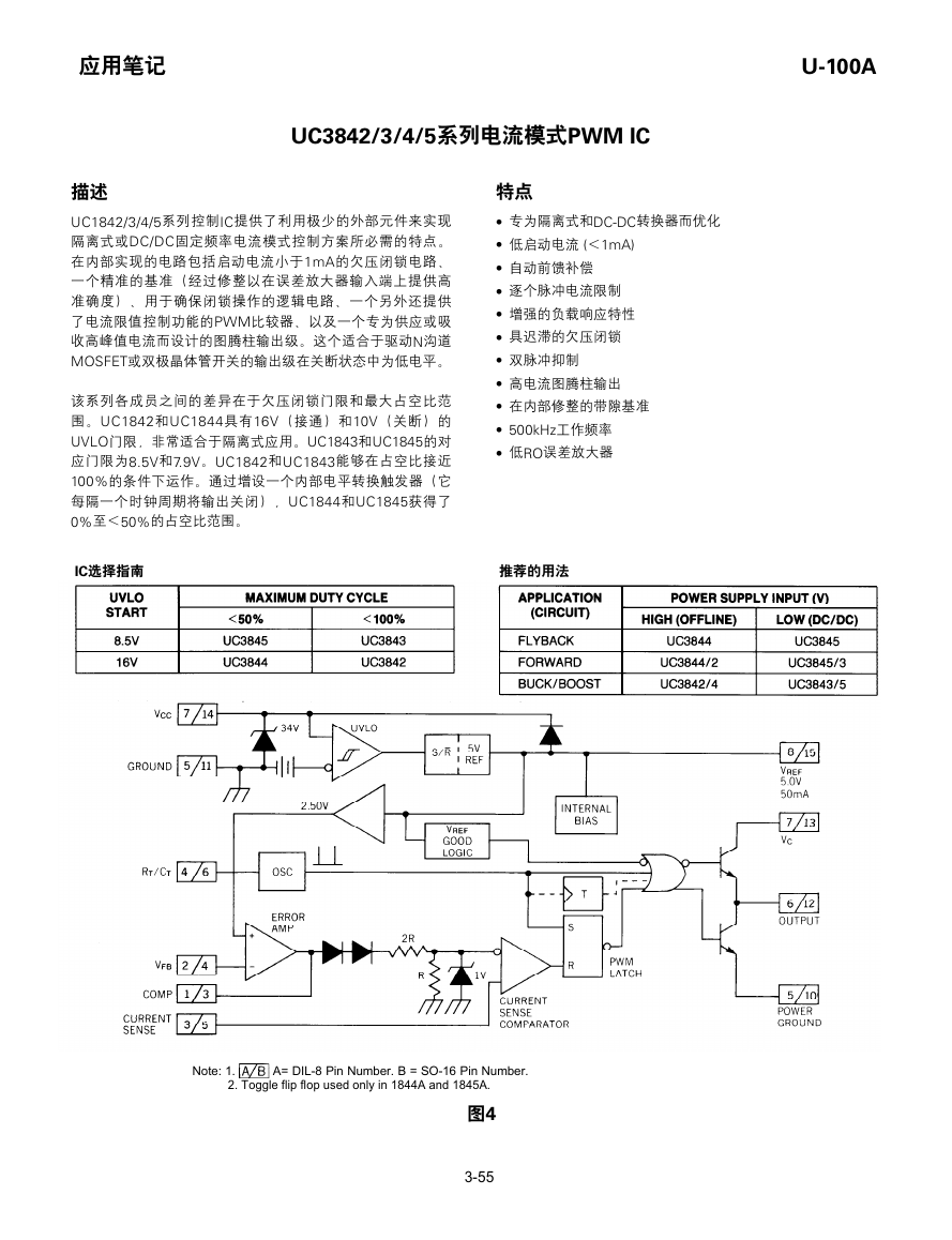
UC1842/3/4/5系列控制IC提供了利用极少的外部元件来实现
clude under-voltage lockout featuring start up current less
隔离式或DC/DC固定频率电流模式控制方案所必需的特点。
than 1 mA, a precision reference trimmed for accuracy at
在内部实现的电路包括启动电流小于1mA的欠压闭锁电路、
the error amp input, logic to insure latched operation, a
一个精准的基准(经过修整以在误差放大器输入端上提供高
PWM comparator which also provides current limit control,
准确度)、用于确保闭锁操作的逻辑电路、一个另外还提供
and a totem pole output stage designed to source or sink
了电流限值控制功能的PWM比较器、以及一个专为供应或吸
high peak current. The output stage, suitable for driving ei-
ther N Channel MOSFETs or bipolar transistor switches, is
收高峰值电流而设计的图腾柱输出级。这个适合于驱动N沟道
low in the off state.
MOSFET或双极晶体管开关的输出级在关断状态中为低电平。
Differences between members of this family are the un-
der-voltage lockout thresholds and maximum duty cycle
该系列各成员之间的差异在于欠压闭锁门限和最大占空比范
ranges. The UC1842 and UC1844 have UVLO thresholds
围。UC1842和UC1844具有16V(接通)和10V(关断)的
of 16V (on) and 10V (off), ideally suited to off-line applica-
UVLO门限,非常适合于隔离式应用。UC1843和UC1845的对
tions. The corresponding thresholds for the UC1843 and
应门限为8.5V和7.9V。UC1842和UC1843能够在占空比接近
UC1845 are 8.5V and 7.9V. The UC1842 and UC1843 can
100%的条件下运作。通过增设一个内部电平转换触发器(它
operate to duty cycles approaching 100%. A range of
每隔一个时钟周期将输出关闭),UC1844和UC1845获得了
zero to <50% is obtained by the UC1844 and UC1845 by
the addition of an internal toggle flip flip which blanks the
0%至<50%的占空比范围。
output off every other clock cycle.
IC SELECTION GUIDE
IC选择指南
FEATURES
Optimized for Off-Line and DC to DC Converters
特点
Low Start Up Current (< 1 mA)
Automatic Feed Forward Compensation
专为隔离式和DC-DC转换器而优化
低启动电流 (<1mA)
Pulse-By-Pulse Current Limiting
自动前馈补偿
Enhanced Load Response Characteristics
逐个脉冲电流限制
Under-Voltage Lockout with Hysteresis
增强的负载响应特性
Double Pulse Suppression
具迟滞的欠压闭锁
High Current Totem Pole Output
双脉冲抑制
Internally Trimmed Bandgap Reference
高电流图腾柱输出
在内部修整的带隙基准
500 kHz Operation
500kHz工作频率
Low
Error Amp
低RO误差放大器
•
•
•
•
•
•
•
•
•
•
•
RECOMMENDED USAGE
推荐的用法
Note: 1.
A= DIL-8 Pin Number. B = SO-16 Pin Number.
2. Toggle flip flop used only in 1844A and 1845A.
Figure 4
图4
3-55
�
APPLICATION NOTE
APPLICATION NOTE
应用笔记
UNDER-VOLTAGE LOCKOUT
is adequate to make
The UVLO circuit insures that
UNDER-VOLTAGE LOCKOUT
fully operational before enabling the
the
output stage. Figure 5 shows that the UVLO turn-on and
欠压闭锁
is adequate to make
The UVLO circuit insures that
turn-off thresholds are fixed internally at 16V and 10V re-
the
fully operational before enabling the
spectively. The 6V hysteresis prevents
oscillations
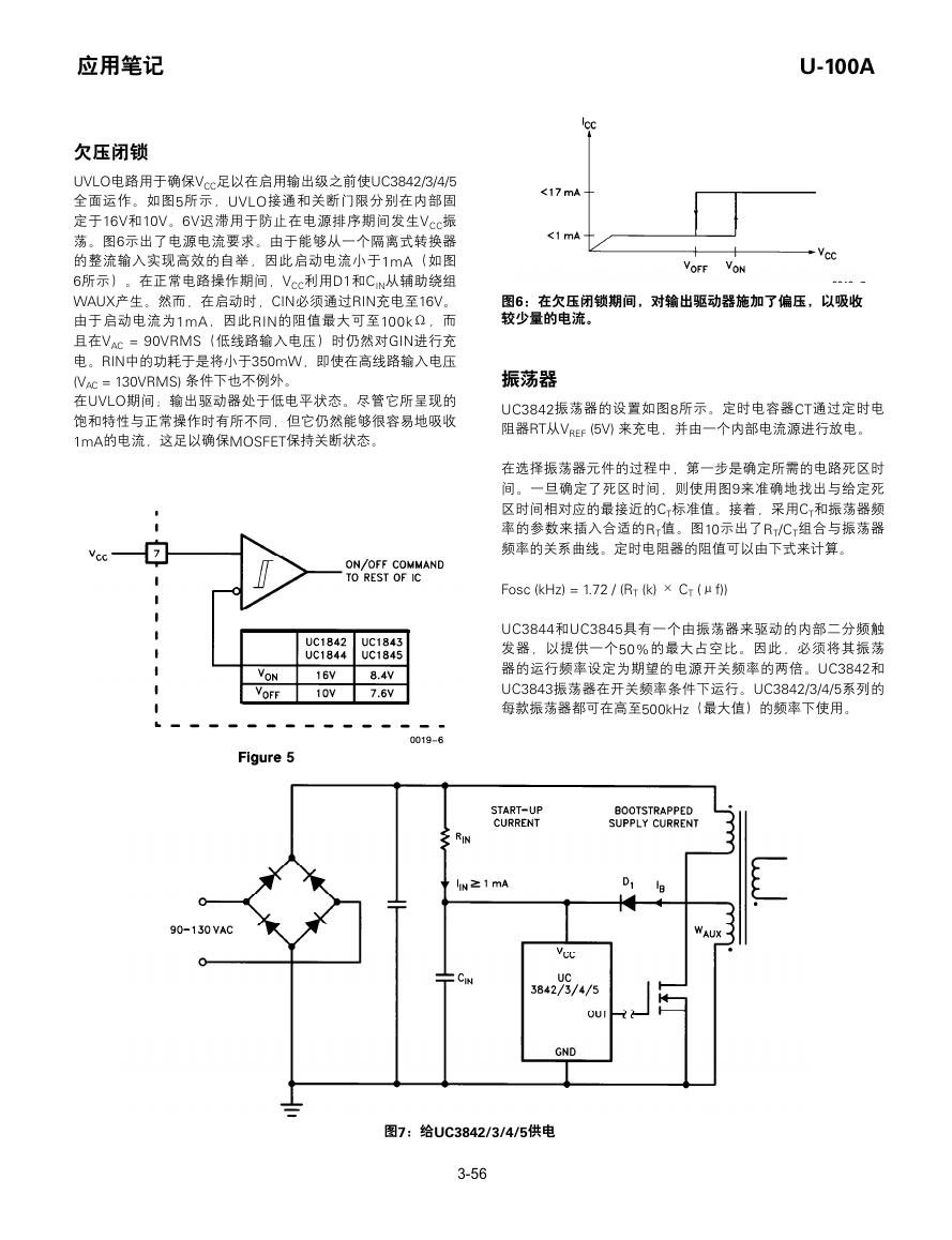
UVLO电路用于确保VCC足以在启用输出级之前使UC3842/3/4/5
output stage. Figure 5 shows that the UVLO turn-on and
during power sequencing. Figure 6 shows supply current
全面运作。如图5所示,UVLO接通和关断门限分别在内部固
turn-off thresholds are fixed internally at 16V and 10V re-
requirements. Start-up current is less than 1 mA for effi-
spectively. The 6V hysteresis prevents
oscillations
定于16V和10V。6V迟滞用于防止在电源排序期间发生VCC振
cient bootstrapping from the rectified input of an off-line
during power sequencing. Figure 6 shows supply current
荡。图6示出了电源电流要求。由于能够从一个隔离式转换器
converter, as illustrated by Figure 6. During normal circuit
requirements. Start-up current is less than 1 mA for effi-
的整流输入实现高效的自举,因此启动电流小于1mA(如图
operation,
cient bootstrapping from the rectified input of an off-line
6所示)。在正常电路操作期间,VCC利用D1和CIN从辅助绕组
with
must be
converter, as illustrated by Figure 6. During normal circuit
WAUX产生。然而,在启动时,CIN必须通过RIN充电至16V。
charged to 16V through
With a start-up current of 1
operation,
mA,
and still charge GIN
由于启动电流为1mA,因此RIN的阻值最大可至100kΩ,而
with
must be
when
= 90V RMS (low line). Power dissipation in
With a start-up current of 1
charged to 16V through
且在VAC = 90VRMS(低线路输入电压)时仍然对GIN进行充
would then be less than 350 mW even under high line
can be as large as 100
mA,
and still charge GIN
电。RIN中的功耗于是将小于350mW,即使在高线路输入电压
= 130V RMS) conditions.
when
= 90V RMS (low line). Power dissipation in
(VAC = 130VRMS) 条件下也不例外。
would then be less than 350 mW even under high line
During UVLO; the output driver is in a low state. While it
在UVLO期间;输出驱动器处于低电平状态。尽管它所呈现的
= 130V RMS) conditions.
doesn’t exhibit the same saturation characteristics as nor-
饱和特性与正常操作时有所不同,但它仍然能够很容易地吸收
mal operation, it can easily sink 1 milliamp, enough to in-
During UVLO; the output driver is in a low state. While it
1mA的电流,这足以确保MOSFET保持关断状态。
sure the MOSFET is held off.
doesn’t exhibit the same saturation characteristics as nor-
mal operation, it can easily sink 1 milliamp, enough to in-
sure the MOSFET is held off.
is developed from auxiliary winding
is developed from auxiliary winding
can be as large as 100
and
At start-up, however,
and
At start-up, however,
U-100A
U-100A
U-100A
U-100A
Figure 6. During Under-Voltage Lockout, the output
driver is biased to sink minor amounts of
current.
Figure 6. During Under-Voltage Lockout, the output
图6:在欠压闭锁期间,对输出驱动器施加了偏压,以吸收
driver is biased to sink minor amounts of
较少量的电流。
OSCILLATOR
current.
The UC3842 oscillator is programmed as shown in Figure
OSCILLATOR
8. Timing capacitor CT is charged from
(5V) through
振荡器
the timing resistor
and discharged by an internal cur-
The UC3842 oscillator is programmed as shown in Figure
rent source.
UC3842振荡器的设置如图8所示。定时电容器CT通过定时电
8. Timing capacitor CT is charged from
(5V) through
the timing resistor
and discharged by an internal cur-
阻器RT从VREF (5V) 来充电,并由一个内部电流源进行放电。
The first step in selecting the oscillator components is to
rent source.
determine the required circuit deadtime. Once obtained,
Figure 9 is used to pinpoint the nearest standard value of
在选择振荡器元件的过程中,第一步是确定所需的电路死区时
The first step in selecting the oscillator components is to
CT for a given deadtime. Next, the appropriate
value is
determine the required circuit deadtime. Once obtained,
间。一旦确定了死区时间,则使用图9来准确地找出与给定死
interpolated using the parameters for
and oscillator
Figure 9 is used to pinpoint the nearest standard value of
区时间相对应的最接近的CT标准值。接着,采用CT和振荡器频
frequency. Figure 10 illustrates the
combinations
CT for a given deadtime. Next, the appropriate
value is
率的参数来插入合适的RT值。图10示出了RT/CT组合与振荡器
versus oscillator frequency. The timing resistor can be cal-
interpolated using the parameters for
and oscillator
频率的关系曲线。定时电阻器的阻值可以由下式来计算。
culated from the following formula.
frequency. Figure 10 illustrates the
combinations
versus oscillator frequency. The timing resistor can be cal-
Fosc (kHz) = 1.72 / (RT (k) × CT (μf))
culated from the following formula.
The UC3844 and UC3845 have an internal divide-by-two
flip-flop driven by the oscillator for a 50% maximum duty
UC3844和UC3845具有一个由振荡器来驱动的内部二分频触
cycle. Therefore, their oscillators must be set to run at
The UC3844 and UC3845 have an internal divide-by-two
发器,以提供一个50%的最大占空比。因此,必须将其振荡
twice the desired power supply switching frequency. The
flip-flop driven by the oscillator for a 50% maximum duty
器的运行频率设定为期望的电源开关频率的两倍。UC3842和
UC3842 and UC3843 oscillator runs AT the switching fre-
cycle. Therefore, their oscillators must be set to run at
UC3843振荡器在开关频率条件下运行。UC3842/3/4/5系列的
quency. Each oscillator of the
family can
twice the desired power supply switching frequency. The
每款振荡器都可在高至500kHz(最大值)的频率下使用。
be used to a maximum of 500 kHz.
UC3842 and UC3843 oscillator runs AT the switching fre-
quency. Each oscillator of the
family can
be used to a maximum of 500 kHz.
(kHz) = 1.72 /
(kHz) = 1.72 /
(k) ×
(k) ×
Figure 7. Providing Power to the
图7:给UC3842/3/4/5供电
Figure 7. Providing Power to the
3-56
3-56
0019-8
0019-8
�
APPLICATION NOTE
APPLICATION NOTE
应用笔记
MAXIMUM DUTY CYCLE
The UC3842 and UC3843 have a maximum duty cycle of
MAXIMUM DUTY CYCLE
最大占空比
approximately 100%, whereas the UC3844 and UC3845
The UC3842 and UC3843 have a maximum duty cycle of
UC3842和UC3843具有约100%的最大占空比,而UC3844和
are clamped to 50% maximum by an internal toggle flip
approximately 100%, whereas the UC3844 and UC3845
flop. This duty cycle clamp is advantageous in most fly-
UC3845的最大占空比则被一个内部电平转换触发器箝位于
are clamped to 50% maximum by an internal toggle flip
back and forward converters. For optimum IC perform-
50%。在大多数反激式和正激式转换器中,这种占空比箝位
flop. This duty cycle clamp is advantageous in most fly-
ance the deadtime should not exceed 15% of the oscilla-
是有好处的。为了获得最佳的IC性能,死区时间不应超过振荡
back and forward converters. For optimum IC perform-
tor clock period.
器时钟周期的15%。
ance the deadtime should not exceed 15% of the oscilla-
During the discharge, or “dead” time, the internal clock
tor clock period.
signal blanks the output to the low state. This limits the
在放电期间(或“死区”时间)里,内部时钟信号将输出锁
During the discharge, or “dead” time, the internal clock
maximum duty cycle
至低电平状态。这将最大占空比DMAX限制为:
signal blanks the output to the low state. This limits the
maximum duty cycle
DMAX = 1 – (tDEAD / tPERIOD) UC3842/3
DMAX = 1 – (tDEAD / 2 x tPERIOD) UC3844/5
式中的tDEAD = 1 / F振荡器
where TPERIOD = 1 / F oscillator
where TPERIOD = 1 / F oscillator
U C 3 8 4 2 / 3
UC3844/5
U C 3 8 4 2 / 3
UC3844/5
= 1 -
= 1 -
= 1 -
= 1 -
/ 2 X
/ 2 X
to:
to:
0019-9
Figure 8
Figure 8
图8
Deadtime vs
Deadtime vs
死区时间与CT的关系曲线 (RT>5k)
> 5k)
> 5k)
0019-9
Figure 9
Figure 9
图9
Timing Resistance vs Frequency
Timing Resistance vs Frequency
定时电阻与频率的关系曲线
0019-10
0019-10
U-100A
U-100A
U-100A
IP =
= control voltage = E/A output voltage.
= control voltage = E/A output voltage.
CURRENT SENSING AND LIMITING
The UC3842 current sense input is configured as shown
CURRENT SENSING AND LIMITING
电流检测和限制
in Figure 12. Current-to-voltage conversion is done exter-
The UC3842 current sense input is configured as shown
UC3842电流检测输入的配置如图12所示。电流-电压转换利
nally with ground-referenced resistor
Under normal
in Figure 12. Current-to-voltage conversion is done exter-
operation the peak voltage across
is controlled by the
用接地参考电阻器RS在外部完成。在正常工作条件下,RS两
Under normal
nally with ground-referenced resistor
E/A according to the following relation:
端的峰值电压受控于E/A(误差放大器),依据的公式如下:
operation the peak voltage across
is controlled by the
E/A according to the following relation:
(VC – 1.4V)
(3 RS)
where
can be connected to the power circuit directly or
where
式中,VC = 控制电压 = E/A输出电压。
through a current transformer, as Figure 11 illustrates.
can be connected to the power circuit directly or
While a direct connection is simpler, a transformer can re-
如图11所示,RS可直接(或通过一个电流变压器)连接至电
through a current transformer, as Figure 11 illustrates.
reduce errors caused by the
duce power dissipation in
While a direct connection is simpler, a transformer can re-
源电路。虽然直接连接的做法比较简单,但采用变压器能够降
base current, and provide level shifting to eliminate the re-
duce power dissipation in
reduce errors caused by the
低RS中的功耗、减少由基极电流引起的误差、并提供电平移
straint of ground-referenced sensing. The relation be-
base current, and provide level shifting to eliminate the re-
位以消除接地参考检测的限制。VC与功率级中的峰值电流之
tween
and peak current in the power stage is given by:
straint of ground-referenced sensing. The relation be-
间的关系由下式给出:
and peak current in the power stage is given by:
tween
VRS(pk)
(
) =
RS 3RS
where: N = current sense transformer turns ratio
= 1 when transformer not used.
式中:N = 电流检测变压器匝数比
where: N = current sense transformer turns ratio
For purposes of small-signal analysis, the control-to-
= 1 when transformer not used.
= 1(当未使用变压器时)。
sensed-current gain is:
For purposes of small-signal analysis, the control-to-
为了便于小信号分析,控制-检测电流增益为:
sensed-current gain is:
( VC – 1.4V )
i(pk) = N
N
=
i(pk) N
When sensing current in series with the power transistor,
VC 3 RS
as shown in Figure 11, the current waveform will often
When sensing current in series with the power transistor,
have a large spike at its leading edge. This is due to recti-
as shown in Figure 11, the current waveform will often
如图11所示,当检测与功率晶体管串联的电流时,电流波形在
fier recovery and/or inter-winding capacitance in the pow-
have a large spike at its leading edge. This is due to recti-
其前沿处常常将出现一个很大的尖峰。这是由于整流器恢复和
er transformer. If unattenuated, this transient can prema-
fier recovery and/or inter-winding capacitance in the pow-
turely terminate the output pulse. As shown, a simple RC
/或电源变压器中的绕组间电容所造成的。如果不对其进行衰
er transformer. If unattenuated, this transient can prema-
filter is usually adequate to suppress this spike. The RC
减,那么该瞬变会过早地终止输出脉冲。如图所示,采用一个
turely terminate the output pulse. As shown, a simple RC
time constant should be approximately equal to the cur-
简单的RC滤波器往往足以抑制该尖峰。RC时间常数应大致等
filter is usually adequate to suppress this spike. The RC
rent spike duration (usually a few hundred nanoseconds).
于电流尖峰持续时间(通常为几百ns)。
time constant should be approximately equal to the cur-
The inverting input to the UC3842 current-sense compara-
rent spike duration (usually a few hundred nanoseconds).
tor is internally clamped to 1V (Figure 12). Current limiting
UC3842电流检测比较器的反相输入在内部箝位于1V(图
The inverting input to the UC3842 current-sense compara-
occurs if the voltage at pin 3 reaches this threshold value,
12)。如果引脚3上的电压达到其门限值,则电流限制电路开
tor is internally clamped to 1V (Figure 12). Current limiting
i.e., the current limit is defined by:
occurs if the voltage at pin 3 reaches this threshold value,
始起作用,也就是说:电流限值由下式决定:
i.e., the current limit is defined by:
N x 1V
RS
imax =
FREOUENCY - (Hz)
Figure 10
FREOUENCY - (Hz)
Figure 10
图10
0019-11
0019-11
0019-13
Figure 11. Transformer-Coupled Current Sensing
0019-13
Figure 11. Transformer-Coupled Current Sensing
3-57
3-57
�
APPLICATION NOTE
应用笔记
U-100A
U-100A
U-100A
Figure 12. Current Sensing
图12:电流检测
0019-12
ERROR AMPLIFIER
误差放大器
The error amplifier (E/A) configuration is shown in Figure
误差放大器 (E/A) 配置示于图13。同相输入未被引出至一个引
13. The non-inverting input is not brought out to a pin, but
脚,而是在内部被施加偏压至2.5V±2%。E/A输出可在引脚1
is internally biased to 2.5V ± 2%. The E/A output is
available at pin 1 for external compensation, allowing the
上提供(用于外部补偿),从而使用户能够控制转换器的闭环
user to control the converter’s closed-loop frequency re-
频率响应。
sponse.
图14示出了一款适合于对任何电流模式控制拓扑结构(利用电
Figure 14 shows an E/A compensation circuit suitable for
stabilizing any current-mode controlled topology except for
感器电流来运作的反激式和升压型转换器除外)进行稳定化处
flyback and boost converters operating with inductor cur-
理的E/A补偿电路。反馈元件给环路转移函数增加了一个极点
rent. The feedback components add a pole to the loop
(在fP = 1/2πRF,CF)。选择合适的RF、CF,以使该极点抵消
transfer function at
are cho-
电源电路中输出滤波电容器ESR的零点。RI和RF固定了低频增
sen so that this pole cancels the zero of the output filter
益。它们的选择依据是:提供尽可能大的增益,同时仍然允许
capacitor ESR in the power circuit.
fix the low-
由输出滤波电容器和负载形成的极点在f ≈ fSWITCHING / 4时将
frequency gain. They are chosen to provide as much gain
as possible while still allowing the pole formed by the out-
环路增益衰减至单位增益 (0dB)。这种方法确保了转换器稳定
put filter capacitor and load to roll off the loop gain to uni-
性,而且还提供了上佳的动态响应。
This technique insures
ty (0 dB) at f
converter stability while providing good dynamic response.
E/A输出将供应0.5mA电流并吸收2mA电流。RF的下限由下式
给出:
and
=
and
Figure 14. Compensation
图14:补偿
The E/A output will source 0.5 mA amd sink 2 mA. A low-
er limit for
is given by:
Figure 13. E/A Configuration
图13:E/A配置
3-58
0019-14
�
max) flows through
given by:
as low as
APPLICATION NOTE
应用笔记
E/A input bias curret (2
result-
ing in a DC error in output voltage
E/A输入偏置电流(最大值为2μA)流过RI,在输出电压 (VO)
中产生了一个DC误差,由下式给出:
It is therefore desirable to keep the value of
ΔVO(MAX) = (2μA) RI,
possible.
Figure 15 shows the open-loop frequency response of the
因此,使RI的阻值尽可能低是合乎需要的。
UC3842 E/A. The gain represents an upper limit on the
gain of the compensated E/A. Phase lag increases rapidly
图15示出了UC3842 E/A的开环频率响应。增益代表了补偿E/
as frequency exceeds 1 MHz due to second-order poles
at ~ 10 MHz and above.
A的增益的上限。由于二阶极点位于约10MHz及更高的频率,
因此当频率超过1MHz时,相位滞后将快速增加。
Continuous-inductor-current boost and flyback converters
each have a right-half-plane zero in their transfer function.
An additional compensation pole is needed to roll off loop
连续电感器电流升压和反激式转换器在其转移函数中均具有
gain at a frequency less than that of the RHP zero.
一个右半平面零点。需要一个额外的补偿极点,以在一个低
and
于RHP零点频率的频率条件下衰减环路增益。图16所示电路
中的RP和CP提供了该极点。
TOTEM-POLE OUTPUT
The UC3842 PWM has a single totem-pole output which
图腾柱输出
can be operated to ± 1 amp peak for driving MOSFET
gates, and a + 200 mA average current for bipolar power
UC3842 PWM具有单个可在至±1A(峰值)的电流条件下运
in the circuit of Figure 16 provide this pole.
U-100A
U-100A
transistors. Cross conduction between the output transis-
tors is minimal, the average added power with
= 30V
作的图腾柱输出(用于驱动MOSFET栅极)和+200mA的平
is only 80 mW at 200 kHz.
均电流(用于驱动双极功率二极管)。输出晶体管之间的交
Limiting the peak current through the IC is accomplished
叉传导极小,VIN = 30V时的平均附加功率仅为80mW(在
by placing a resistor between the totem-pole output and
200kHz)。
the gate of the MOSFET. The value is determined by di-
viding the totem-pole collector voltage
by the peak
对流过IC的峰值电流的限制是通过在图腾柱输出和MOSFET的
current rating of the IC’s totem-pole. Without this resistor,
the peak current is limited only by the dV/dT rate of the
栅极之间布设一个电阻器来完成的。电流限值由“图腾柱集电
totem-pole switching and the FET gate capacitance.
极电压VC÷IC图腾柱的额定峰值电流”来确定。未采用该电阻
器时,峰值电流仅受限于图腾柱开关操作的dV/dT速率和FET
The use of a Schottky diode from the PWM output to
栅极电容。
ground will prevent the output voltage from going exces-
sively below ground, causing instabilities within the IC. To
be effective, the diode selected should have a forward
通过在PWM输出和地之间采用一个肖特基二极管,将防止输
drop of less than 0.3V at 200 mA. Most l- to 3-amp
出电压变至过分低于地电位的电平而在IC内部导致不稳定。为
Schottky diodes exhibit these traits above room tempera-
了发挥效用,所选择的二极管在200mA的电流条件下应具有小
ture. Placing the diode as physically close to the PWM as
于0.3V的正向压降。大多数1~3A肖特基二极管在高于室温的
possible will enhance circuit performance. Implementation
条件下均呈现出这些特征。把二极管布设在尽可能靠近PWM
of the complete drive scheme is shown in the following di-
agrams. Transformer driven circuits also require the use of
的地方将增强电路性能。完整驱动电路的可实现方案见下面的
the Schottky diodes to prevent a similar set of circum-
示意图。由变压器驱动的电路也需要使用肖特基二极管,以防
止在PWM输出端上出现相似的情形。(接下页)
10
100
1K
10K
100K
1M
10M
Figure 15. Error Amplifier Open-Loop Frequency Response
图15:误差放大器开环频率响应
FREQUENCY - (Hz)
0019-16
Figure 16. E/A Compensation Circuit for Continuous Boost and Flyback Topologies
0019-17
图16:针对连续升压和反激式拓扑结构的E/A补偿电路
3-59
�
APPLICATION NOTE
APPLICATION NOTE
应用笔记
stances from occurring on the PWM output. The ringing
stances from occurring on the PWM output. The ringing
below ground is greatly enhanced by the transformer leak-
below ground is greatly enhanced by the transformer leak-
(接上页)除了磁化电感和FET栅极电容之外,变压器漏电感
age inductance and parasitic capacitance, in addition to
age inductance and parasitic capacitance, in addition to
the magnetizing inductance and FET gate capacitance.
和寄生电容也极大地增强了低于地电位的振铃。电路实现方案
the magnetizing inductance and FET gate capacitance.
Circuit implementation is similar to the previous example.
Circuit implementation is similar to the previous example.
与前一个例子很相似。
Figures 18, 19 and 20 show suggested circuits for driving
Figures 18, 19 and 20 show suggested circuits for driving
MOSFETs and bipolar transistors with the UC3842 output.
图18、19和20示出了适合于采用UC3842输出来驱动MOSFET
MOSFETs and bipolar transistors with the UC3842 output.
The simple circuit of Figure 18 can be used when the
The simple circuit of Figure 18 can be used when the
和双极晶体管的推荐电路。当控制IC与MOSFET接通和关断电
control IC is not electrically isolated from the MOSFET
control IC is not electrically isolated from the MOSFET
隔离未达到±1A时,可以采用图18中的简单电路。它还为一
turn-on and turn-off to ± 1 amp. It also provides damping
turn-on and turn-off to ± 1 amp. It also provides damping
个由FET输入电容和串联导线电感组成的寄生谐振电路提供了
for a parasitic tank circuit formed by the FET input capaci-
for a parasitic tank circuit formed by the FET input capaci-
阻尼。肖特基二极管D1用于防止IC的输出在关断期间变至远
tance and series wiring inductance. Schottky diode D1
tance and series wiring inductance. Schottky diode D1
远低于地电位的电平。
prevents the output of the IC from going far below ground
prevents the output of the IC from going far below ground
during turn-off.
during turn-off.
图19示出了一款隔离式MOSFET驱动电路,当驱动信号必须进
U-100A
U-100A
U-100A
U-100A
Figure 19 shows an isolated MOSFET drive circuit which
Figure 19 shows an isolated MOSFET drive circuit which
is appropriate when the drive signal must be level shifted
is appropriate when the drive signal must be level shifted
or transmitted across an isolation boundary. Bipolar tran-
行电平移位或穿越一个隔离边界进行传输时,很适合采用该电
or transmitted across an isolation boundary. Bipolar tran-
sistors can be driven efficiently with the circuit of Figure
路。利用图20所示的电路可以高效地驱动双极晶体管。电阻器
sistors can be driven efficiently with the circuit of Figure
20. Resistors
fix the on-state base current
and
and
fix the on-state base current
20. Resistors
R1和R2负责固定通态基极电流,而电容器C1则提供了一个负基
while capacitor
provides a negative base current pulse
while capacitor
provides a negative base current pulse
极电流脉冲,以在关断时清除累积电荷。
to remove stored charge at turn-off.
to remove stored charge at turn-off.
Since the UC3842 series has only a single output, an in-
Since the UC3842 series has only a single output, an in-
由于UC3842系列只具有单个输出,因此需要一个接口电路来
terface circuit is needed to control push-pull half or full
terface circuit is needed to control push-pull half or full
控制推挽半桥式或全桥式拓扑结构。具有内部电平转换触发器
bridge topologies. The UC3706 dual output driver with in-
bridge topologies. The UC3706 dual output driver with in-
的UC3706双路输出驱动器负责执行此项功能。本文末尾所举
ternal toggle flip-flop performs this function. A circuit ex-
ternal toggle flip-flop performs this function. A circuit ex-
的电路实例示出了这两款IC的一种典型应用。采用UC3705/6/7
ample at the end of this paper illustrates a typical applica-
ample at the end of this paper illustrates a typical applica-
驱动器IC当中的一款,就能够实现更强的驱动能力,以驱动多
tion for these two ICs. Increased drive capability for driv-
tion for these two ICs. Increased drive capability for driv-
ing numerous FETs in parallel, or other loads can be ac-
个并联的FET或其他负载。
ing numerous FETs in parallel, or other loads can be ac-
complished using one of the UC3705/6/7 driver ICs.
complished using one of the UC3705/6/7 driver ICs.
10 TO 20V
10 TO 20V
OUTPUT CURRENT SOURCE OR SINK - (A)
OUTPUT CURRENT SOURCE OR SINK - (A)
Figure 17. Output Saturation Characteristics
Figure 17. Output Saturation Characteristics
图17:输出饱和特性
0019-18
0019-18
图18:直接MOSFET驱动
Figure 18. Direct MOSFET Drive
Figure 18. Direct MOSFET Drive
20 TO 30V
20 TO 30V
12 TO 20V
12 TO 20V
Figure 19. Isolated MOSFET Drive
Figure 19. Isolated MOSFET Drive
图19:隔离式MOSFET驱动
Figure 20. Bipolar Drive with Negative Turn-Off Bias
Figure 20. Bipolar Drive with Negative Turn-Off Bias
图20:采用负关断偏压的双极驱动
3-61
3-61
�


 2023年江西萍乡中考道德与法治真题及答案.doc
 2012年重庆南川中考生物真题及答案.doc
 2013年江西师范大学地理学综合及文艺理论基础考研真题.doc
 2020年四川甘孜小升初语文真题及答案I卷.doc
 2020年注册岩土工程师专业基础考试真题及答案.doc
 2023-2024学年福建省厦门市九年级上学期数学月考试题及答案.doc
 2021-2022学年辽宁省沈阳市大东区九年级上学期语文期末试题及答案.doc
 2022-2023学年北京东城区初三第一学期物理期末试卷及答案.doc
 2018上半年江西教师资格初中地理学科知识与教学能力真题及答案.doc
 2012年河北国家公务员申论考试真题及答案-省级.doc
 2020-2021学年江苏省扬州市江都区邵樊片九年级上学期数学第一次质量检测试题及答案.doc
 2022下半年黑龙江教师资格证中学综合素质真题及答案.doc