TPR_C101_V20
Page 1 of 15
Proposed
Draft
Serial ATA
International Organization
Revision 20
September 9, 2009
SATA30_TPR_C101_V20
Title: mSATA Connector
This is an internal working document of the Serial ATA International Organization. As such, this is
not a completed standard and has not been approved. The Serial ATA International Organization
may modify the contents at any time. This document is made available for review and comment
only.
Permission is granted to the Promoters, Contributors and Adopters of the Serial ATA International
Organization to reproduce this document for the purposes of evolving the technical content for
internal use only without further permission provided this notice is included. All other rights are
reserved and may be covered by one or more Non Disclosure Agreements including the Serial
ATA International Organization participant agreements. Any commercial or for-profit replication or
republication is prohibited. Copyright © 2000-2009 Serial ATA International Organization. All
rights reserved.
�
TPR_C101_V20
Page 2 of 15
IS PROVIDED
This Draft Specification is NOT the final version of the Specification and is subject to change
without notice. A modified, final version of this Specification (“Final Specification”) when approved
by the Promoters will be made available for download at this Web Site: http://www.serialata.org.
IS” WITH NO WARRANTIES
THIS DRAFT SPECIFICATION
WHATSOEVER,
INCLUDING ANY WARRANTY OF MERCHANTABILITY, NON-
INFRINGEMENT, FITNESS FOR ANY PARTICULAR PURPOSE OR ANY WARRANTY
OTHERWISE ARISING OUT OF ANY PROPOSAL, SPECIFICATION, OR SAMPLE. Except for
the right to download for internal review, no license, express or implied, by estopple or otherwise,
to any intellectual property rights is granted or intended hereunder.
THE PROMOTERS DISCLAIM ALL LIABILITY, INCLUDING LIABILITY FOR INFRINGEMENT
OF ANY PROPRIETARY RIGHTS, RELATING TO USE OF INFORMATION IN THIS DRAFT
SPECIFICATION. THE PROMOTERS DO NOT WARRANT OR REPRESENT THAT SUCH
USE WILL NOT INFRINGE SUCH RIGHTS.
THIS DOCUMENT IS AN INTERMEDIATE DRAFT FOR COMMENT ONLY AND IS SUBJECT
TO CHANGE WITHOUT NOTICE.
* Other brands and names are the property of their respective owners.
Copyright © 2005-2009 Serial ATA International Organization. All rights reserved.
SATA-IO CabCon Chair:
“AS
Frank Chu
Hitachi Global Storage Technologies
3403 Yerba Buena Road
San Jose, CA 95135 USA
Tel: (408) 717-5224
Email: Frank.Chu@Hitachigst.com
�
TPR_C101_V20
Page 3 of 15
Author Information
Author Name
Jeffrey Hobbet
Edward Chang
Edmund Poh
Company
Lenovo
Samsung
Molex
Email address
jrhobbet@lenovo.com
Ed.chang@sisa.samsung.com
Edmund.Poh@molex.com
Workgroup Chair Information
Workgroup
Chairperson Name
Email address
Frank Chu
Frank.Chu@Hitachigst.com
CabCon
Revision History
Revision
3
4
5
6
7
8
9
10
11
12
13
14
15
16
17
18
19
20
Date
10/09/2008
11/19/2008
11/20/2008
7/21/2009
7/22/2009
8/4/2009
8/4/2009
8/5/2009
8/12/2009
9/2/2009
9/3/2009
9/4/2009
9/4/2009
9/7/2009
9/8/2009
9/8/2009
9/9/2009
9/9/2009
Comments
Initial Proposal to Suppliers
Swapped +B and –B signals to correspond better to typical SATA-IO
PCBA layouts.
Moved pin 1 SATA assignment to Pin 30
Moved pin 20 SATA assignment to Pin 32
Updated references to mSATA
Update pin assignments to have DA/DSS on pin 49 and PD on pin 51
Updated pin table to specify “Host” side for Transmitter/Receiver
Removed references to PCIe
Renamed to TPR_C101 and added compliance point figure
Added Vendor Pins pin 45, 30, 32
Added two wire interface notes for pins 30 and 32.
Editorial clean up
Adding Lab Loads and Compliance Points
Replaced Figure 1
Adding mSATA connector drawings
Editorial changes
Editorial changes
Receptacle to Plug
Editorial changes suggested by Alvin Cox
Editorial changes on Figures
Editorial changes, adding references to JC11-MO-XXX and JC11 SO-
XXX
for Figure 124+2 and Figure 125+2, replace
�
TPR_C101_V20
Page 4 of 15
Introduction
This proposal is intended to define a new electrical pin-out to allow SATA to be delivered across
an mSATA interface connector. This will enable the use of SATA protocol in small form-factor
applications where the connectors are readily available in the industry. This proposal is being
presented by Lenovo on behalf of Lenovo, SanDisk, Samsung, STEC, and Toshiba.
�
TPR_C101_V20
Page 5 of 15
Internal mSATA Connector
1
This section defines the requirements of an mSATA configuration with a Serial-ATA interface.
The definition supports the following capabilities:
• Supports Gen1 (1.5 Gbps) and Gen2 (3 Gbps) transfer rates
• Support for mSATA
• Support of 3.3 V
• Support 4 vendor pins
• Support 2 vendor pins, for drive or SSD manufacturing usage
mSATA
5.2.10
1.1 Usage model
The internal mSATA connector is to be used for embedded applications, part of SATA Rev 3 section
5.2.10 Mobile Applications.
(Proposed to be added to Table 2 in the SATA Rev 3 spec – Usage Model Descriptions)
Characteristic
Use model section number
Cable and/or backplane type
Cable length
Cable Electrical
Attenuation at 4.5GHz
Host-side connector
Device-side connector
Gen 1i 1.5Gbps
Gen 1m 1.5Gbps
Gen 2i 3.0Gbps
Gen 2m 3.0Gbps
Gen1x 1.5Gbps
Gen 2x 3.0Gbps
Hot plug support
(To be defined)
(To be defined)
BP
P
P
R
NS
FS
NS
NS
NS
NS
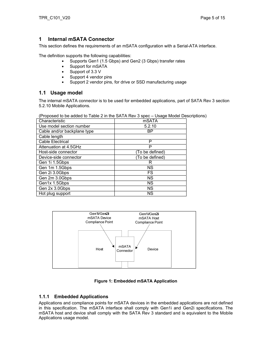
Figure 1: Embedded mSATA Application
1.1.1 Embedded Applications
Applications and compliance points for mSATA devices in the embedded applications are not defined
in this specification. The mSATA interface shall comply with Gen1i and Gen2i specifications. The
mSATA host and device shall comply with the SATA Rev 3 standard and is equivalent to the Mobile
Applications usage model.
�
TPR_C101_V20
Page 6 of 15
1.1.1.1.1 mSATA Lab Load:
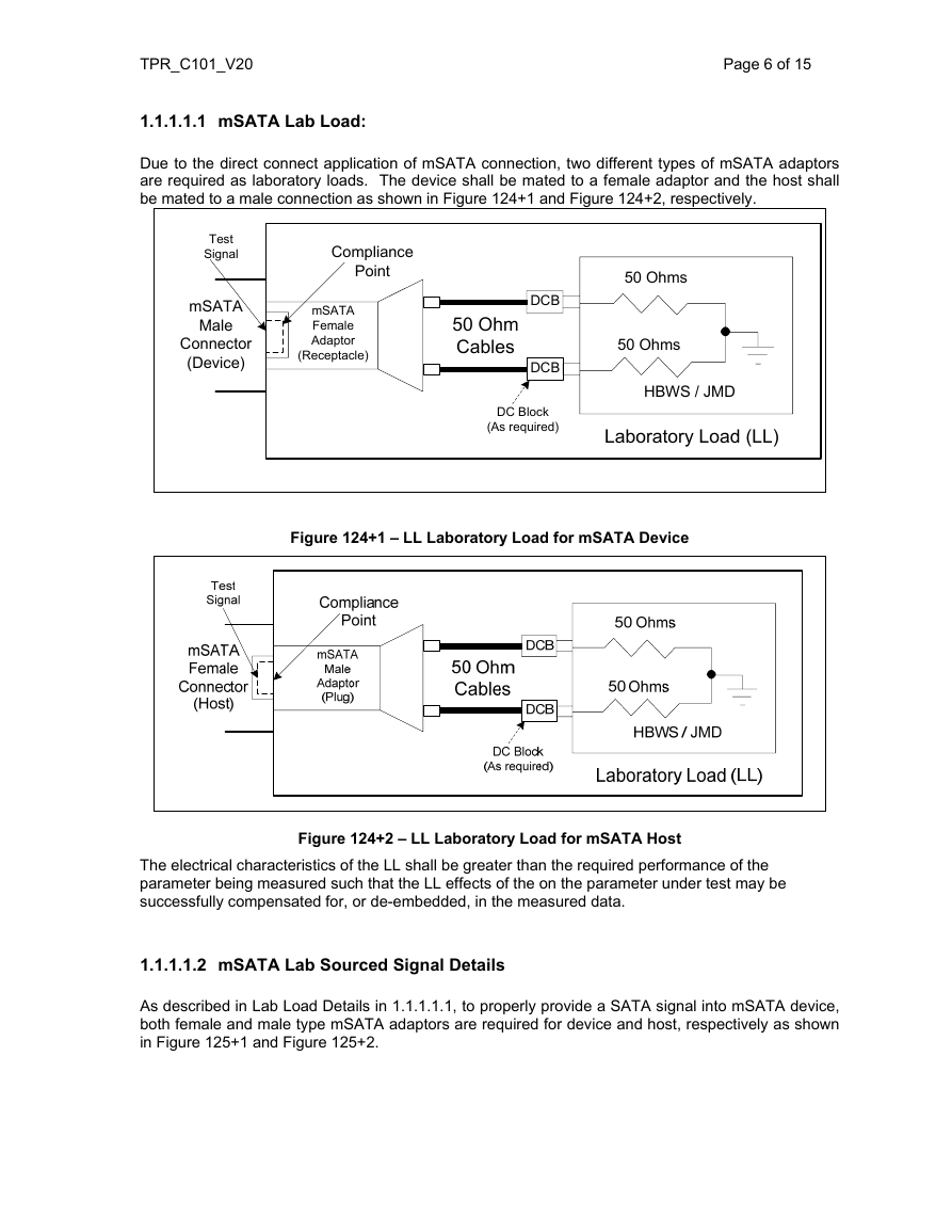
Due to the direct connect application of mSATA connection, two different types of mSATA adaptors
are required as laboratory loads. The device shall be mated to a female adaptor and the host shall
be mated to a male connection as shown in Figure 124+1 and Figure 124+2, respectively.
Test
Signal
mSATA
Male
Connector
(Device)
Compliance
Point
mSATA
Female
Adaptor
(Receptacle)
50 Ohms
50 Ohms
HBWS / JMD
Laboratory Load (LL)
50 Ohm
Cables
DCB
DCB
DC Block
(As required)
Figure 124+1 – LL Laboratory Load for mSATA Device
Figure 124+2 – LL Laboratory Load for mSATA Host
The electrical characteristics of the LL shall be greater than the required performance of the
parameter being measured such that the LL effects of the on the parameter under test may be
successfully compensated for, or de-embedded, in the measured data.
1.1.1.1.2 mSATA Lab Sourced Signal Details
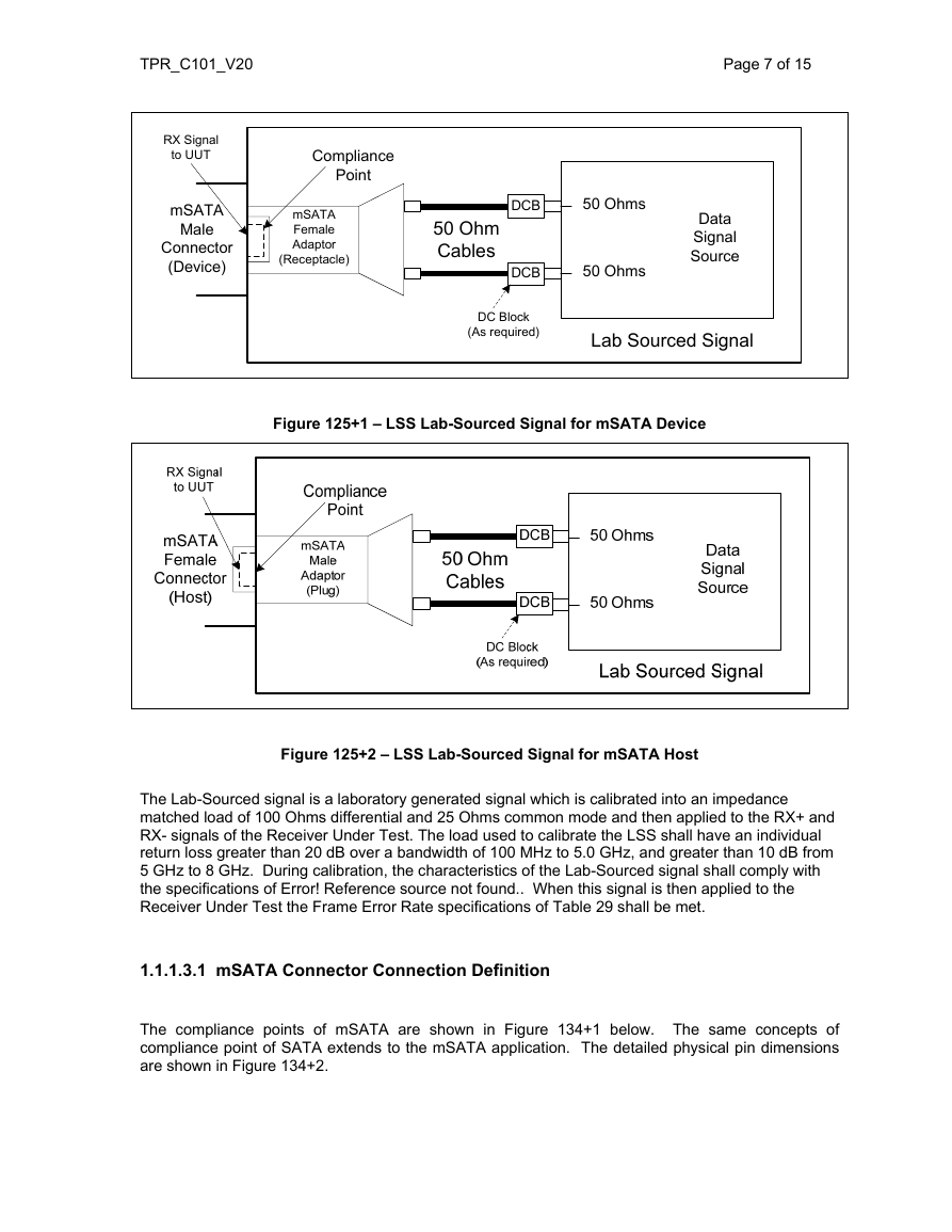
As described in Lab Load Details in 1.1.1.1.1, to properly provide a SATA signal into mSATA device,
both female and male type mSATA adaptors are required for device and host, respectively as shown
in Figure 125+1 and Figure 125+2.
�
TPR_C101_V20
RX Signal
to UUT
mSATA
Male
Connector
(Device)
Page 7 of 15
Compliance
Point
mSATA
Female
Adaptor
(Receptacle)
50 Ohm
Cables
DCB
50 Ohms
DCB
50 Ohms
Data
Signal
Source
DC Block
(As required)
Lab Sourced Signal
Figure 125+1 – LSS Lab-Sourced Signal for mSATA Device
Figure 125+2 – LSS Lab-Sourced Signal for mSATA Host
The Lab-Sourced signal is a laboratory generated signal which is calibrated into an impedance
matched load of 100 Ohms differential and 25 Ohms common mode and then applied to the RX+ and
RX- signals of the Receiver Under Test. The load used to calibrate the LSS shall have an individual
return loss greater than 20 dB over a bandwidth of 100 MHz to 5.0 GHz, and greater than 10 dB from
5 GHz to 8 GHz. During calibration, the characteristics of the Lab-Sourced signal shall comply with
the specifications of Error! Reference source not found.. When this signal is then applied to the
Receiver Under Test the Frame Error Rate specifications of Table 29 shall be met.
1.1.1.3.1 mSATA Connector Connection Definition
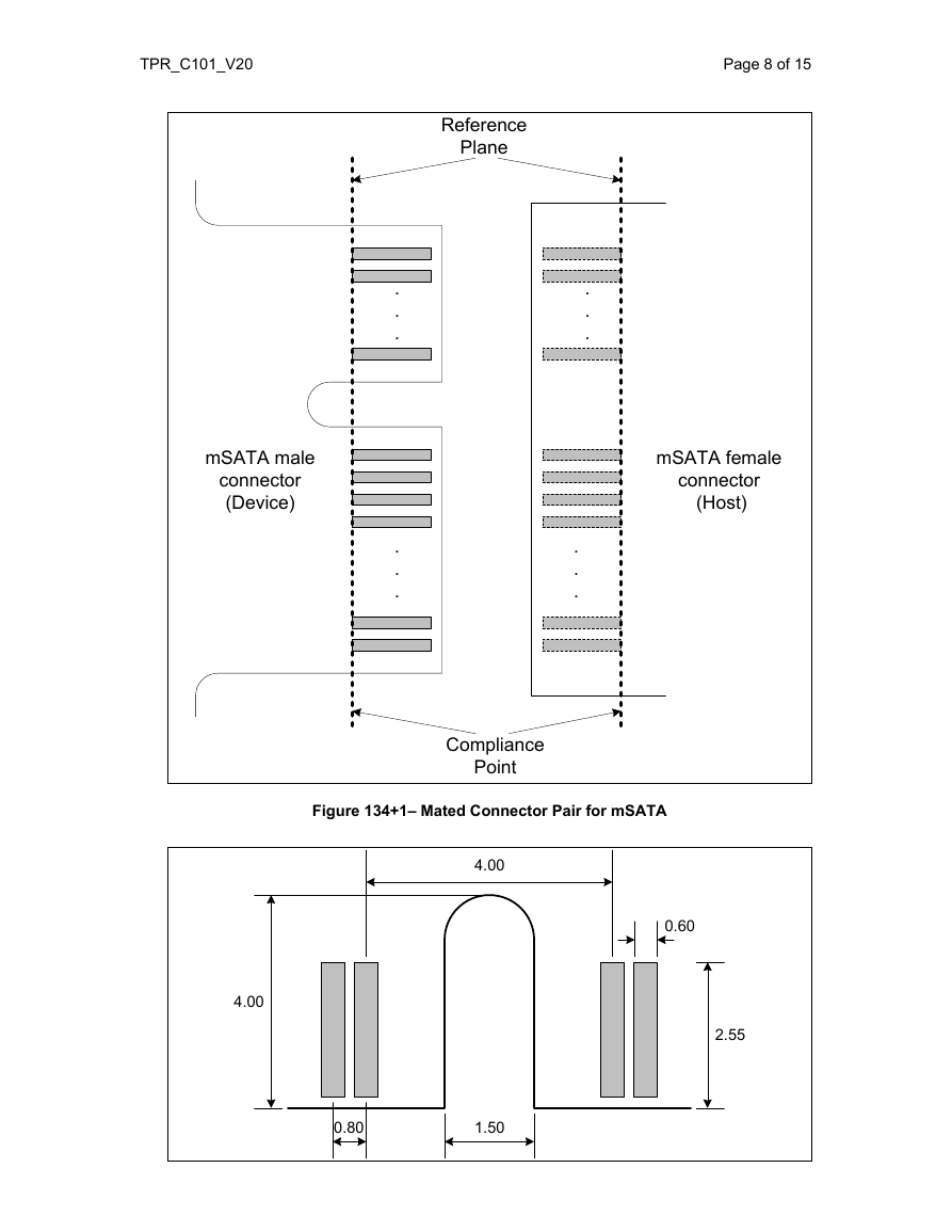
The compliance points of mSATA are shown in Figure 134+1 below. The same concepts of
compliance point of SATA extends to the mSATA application. The detailed physical pin dimensions
are shown in Figure 134+2.
�
TPR_C101_V20
Reference
Plane
Page 8 of 15
.
.
.
.
.
.
mSATA male
connector
(Device)
.
.
.
.
.
.
mSATA female
connector
(Host)
Compliance
Point
Figure 134+1– Mated Connector Pair for mSATA
4.00
4.00
0.80
1.50
0.60
2.55
�



 2023年江西萍乡中考道德与法治真题及答案.doc
 2012年重庆南川中考生物真题及答案.doc
 2013年江西师范大学地理学综合及文艺理论基础考研真题.doc
 2020年四川甘孜小升初语文真题及答案I卷.doc
 2020年注册岩土工程师专业基础考试真题及答案.doc
 2023-2024学年福建省厦门市九年级上学期数学月考试题及答案.doc
 2021-2022学年辽宁省沈阳市大东区九年级上学期语文期末试题及答案.doc
 2022-2023学年北京东城区初三第一学期物理期末试卷及答案.doc
 2018上半年江西教师资格初中地理学科知识与教学能力真题及答案.doc
 2012年河北国家公务员申论考试真题及答案-省级.doc
 2020-2021学年江苏省扬州市江都区邵樊片九年级上学期数学第一次质量检测试题及答案.doc
 2022下半年黑龙江教师资格证中学综合素质真题及答案.doc