Application Report
SCHA002A - February 2003
CD4046B Phase-Locked Loop: A Versatile Building
Block for Micropower Digital and Analog Applications
Standard Linear & Logic
David K. Morgan
ABSTRACT
Applications of the CD4046B phase-locked loop device, such as FM demodulation, FSK
demodulation,
frequency multiplication, signal conditioning, clock
frequency synthesis, are discussed. The monolithic-form
synchronization, and
low-power-consumption CD4046B particularly
in portable
battery-powered equipment.
tone decoding,
is desirable
for use
Contents
1
2
3
4
Introduction
Review of PLL Fundamentals
CD4046B PLL Technical Description
3.1 Phase Comparators
3.2 Voltage-Controlled Oscillator (VCO)
3.3 CD4046B PLL Performance Summary
CD4046B PLL Applications
4.1 FM Demodulation
4.2 Frequency Synthesizer
4.3 Split-Phase Data Synchronization and Decoding
4.4 PLL Lock Detection
. . . . . . . . . . . . . . . . . . . . . . . . . . . . . . . . . . . . . . . . . . . . . . . . . . . . . . . . . . . . . . . . . . . . . . . . .
. . . . . . . . . . . . . . . . . . . . . . . . . . . . . . . . . . . . . . . . . . . . . . . . . . . . . . . . .
. . . . . . . . . . . . . . . . . . . . . . . . . . . . . . . . . . . . . . . . . . . . . . . . . .
. . . . . . . . . . . . . . . . . . . . . . . . . . . . . . . . . . . . . . . . . . . . . . . . . . . . . . . . . . . . . .
. . . . . . . . . . . . . . . . . . . . . . . . . . . . . . . . . . . . . . . . . . . . . . . .
. . . . . . . . . . . . . . . . . . . . . . . . . . . . . . . . . . . . . . . . . . . . .
. . . . . . . . . . . . . . . . . . . . . . . . . . . . . . . . . . . . . . . . . . . . . . . . . . . . . . . . . .
. . . . . . . . . . . . . . . . . . . . . . . . . . . . . . . . . . . . . . . . . . . . . . . . . . . . . . . . . . . . . . .
. . . . . . . . . . . . . . . . . . . . . . . . . . . . . . . . . . . . . . . . . . . . . . . . . . . . . . . . . . .
. . . . . . . . . . . . . . . . . . . . . . . . . . . . . . . . . . . . .
. . . . . . . . . . . . . . . . . . . . . . . . . . . . . . . . . . . . . . . . . . . . . . . . . . . . . . . . . . . . . .
3
3
4
5
11
12
17
17
19
20
21
1
�
SCHA002A
List of Figures
1 PLL Block Diagram
2 CD4046B PLL Block Diagram
3 CD4046B PLL Phase Comparator Section Schematic
4 Phase Comparator I Characteristics at LPF Output
5 Typical Waveforms for CD4046B PLL Employing Phase Comparator I
. . . . . . . . . . . . . . . . . . . . . . . . . . . . . . . . . . . . . . . . . . . . . . . . . . . . . . . . . . . . . . . . . . . . . .
. . . . . . . . . . . . . . . . . . . . . . . . . . . . . . . . . . . . . . . . . . . . . . . . . . . . . . . . . . . .
. . . . . . . . . . . . . . . . . . . . . . . . . . . . . . . . . . . . . . .
. . . . . . . . . . . . . . . . . . . . . . . . . . . . . . . . . . . . . . . . . .
3
4
5
6
in Locked Condition of fo
. . . . . . . . . . . . . . . . . . . . . . . . . . . . . . . . . . . . . . . . . . . . . . . . . . . . . . . . . . . . . . .
7
6 Typical Waveforms for CD4046B PLL Employing Phase Caparator II
in Locked Condition
7 Phase Comparator II State Diagram
8 CD4046B VCO Section Schematic
9 Component-Selection Criteria
10 FM Demodulator
11 FM Demodulator Voltage Waveforms
12 Low-Frequency Synthesizer with Three-Decade Programmable Divider
13 Frequency-Synthesizer Waveforms
14 Split-Phase Data Synchronization and Decoding
15 Lock-Detection Circuit
16 Lock-Detection-Circuit Waveforms
. . . . . . . . . . . . . . . . . . . . . . . . . . . . . . . . . . . . . . . . . . . . . . . . . . . . . . . . . . . . . . . . . . .
. . . . . . . . . . . . . . . . . . . . . . . . . . . . . . . . . . . . . . . . . . . . . . . . . . . . . . .
. . . . . . . . . . . . . . . . . . . . . . . . . . . . . . . . . . . . . . . . . . . . . . . . . . . . . . .
. . . . . . . . . . . . . . . . . . . . . . . . . . . . . . . . . . . . . . . . . . . . . . . . . . . . . . . . . . .
. . . . . . . . . . . . . . . . . . . . . . . . . . . . . . . . . . . . . . . . . . . . . . . . . . . . . . . . . . . . . . . . . . . . . .
. . . . . . . . . . . . . . . . . . . . . . . . . . . . . . . . . . . . . . . . . . . . . . . . . . . .
. . . . . . . . . . . . . . . . . . . . . .
. . . . . . . . . . . . . . . . . . . . . . . . . . . . . . . . . . . . . . . . . . . . . . . . . . . . .
. . . . . . . . . . . . . . . . . . . . . . . . . . . . . . . . . . . . . . . . . .
. . . . . . . . . . . . . . . . . . . . . . . . . . . . . . . . . . . . . . . . . . . . . . . . . . . . . . . . . . . . . . . . .
. . . . . . . . . . . . . . . . . . . . . . . . . . . . . . . . . . . . . . . . . . . . . . . . . . . . . .
8
9
11
16
17
18
19
20
21
22
23
List of Tables
1 Maximum Ratings and General Operating Characteristics
2 VCO Electrical Characteristics
3 Comparator Electrical Characteristics
4 Phase Comparator Comparison
. . . . . . . . . . . . . . . . . . . . . . . . . . . . . . . . . . .
. . . . . . . . . . . . . . . . . . . . . . . . . . . . . . . . . . . . . . . . . . . . . . . . . . . . . . . . . .
. . . . . . . . . . . . . . . . . . . . . . . . . . . . . . . . . . . . . . . . . . . . . . . . . . . .
. . . . . . . . . . . . . . . . . . . . . . . . . . . . . . . . . . . . . . . . . . . . . . . . . . . . . . . . . .
13
13
14
15
2
CD4046B Phase-Locked Loop: A Versatile Building Block for Micropower Digital and Analog Applications
�
1
Introduction
SCHA002A
Phase-locked loops (PLLs), especially in monolithic form, have significantly increased use in
signal-processing and digital systems. Frequency modulation (FM) demodulation, frequency
shift keying (FSK) demodulation, tone decoding, frequency multiplication, signal conditioning,
clock synchronization, and frequency synthesis are some of the many applications of a PLL. The
PLL described in this application report is the CD4046B, which consumes only 600 µW of power
at 10 kHz, a reduction in power consumption of 160 times when compared to the 100 mW
required by similar monolithic bipolar PLLs. This power reduction has particular significance for
portable battery-operated equipment. This application report discusses the basic fundamentals
of PLLs, and presents a detailed technical description of the CD4046B, as well as some of its
applications.
2
Review of PLL Fundamentals
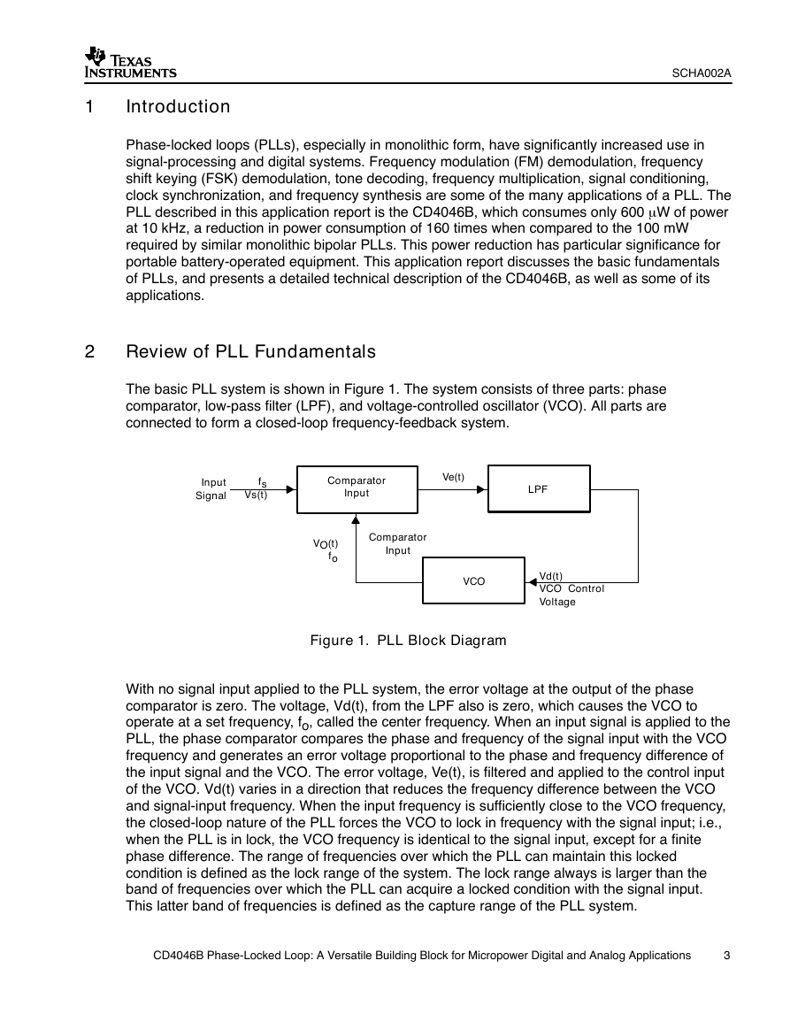
The basic PLL system is shown in Figure 1. The system consists of three parts: phase
comparator, low-pass filter (LPF), and voltage-controlled oscillator (VCO). All parts are
connected to form a closed-loop frequency-feedback system.
Input
Signal
fs
Vs(t)
Comparator
Input
Ve(t)
LPF
VO(t)
fo
Comparator
Input
VCO
Vd(t)
VCO Control
Voltage
Figure 1. PLL Block Diagram
With no signal input applied to the PLL system, the error voltage at the output of the phase
comparator is zero. The voltage, Vd(t), from the LPF also is zero, which causes the VCO to
operate at a set frequency, fo, called the center frequency. When an input signal is applied to the
PLL, the phase comparator compares the phase and frequency of the signal input with the VCO
frequency and generates an error voltage proportional to the phase and frequency difference of
the input signal and the VCO. The error voltage, Ve(t), is filtered and applied to the control input
of the VCO. Vd(t) varies in a direction that reduces the frequency difference between the VCO
and signal-input frequency. When the input frequency is sufficiently close to the VCO frequency,
the closed-loop nature of the PLL forces the VCO to lock in frequency with the signal input; i.e.,
when the PLL is in lock, the VCO frequency is identical to the signal input, except for a finite
phase difference. The range of frequencies over which the PLL can maintain this locked
condition is defined as the lock range of the system. The lock range always is larger than the
band of frequencies over which the PLL can acquire a locked condition with the signal input.
This latter band of frequencies is defined as the capture range of the PLL system.
CD4046B Phase-Locked Loop: A Versatile Building Block for Micropower Digital and Analog Applications
3
�
SCHA002A
3
CD4046B PLL Technical Description
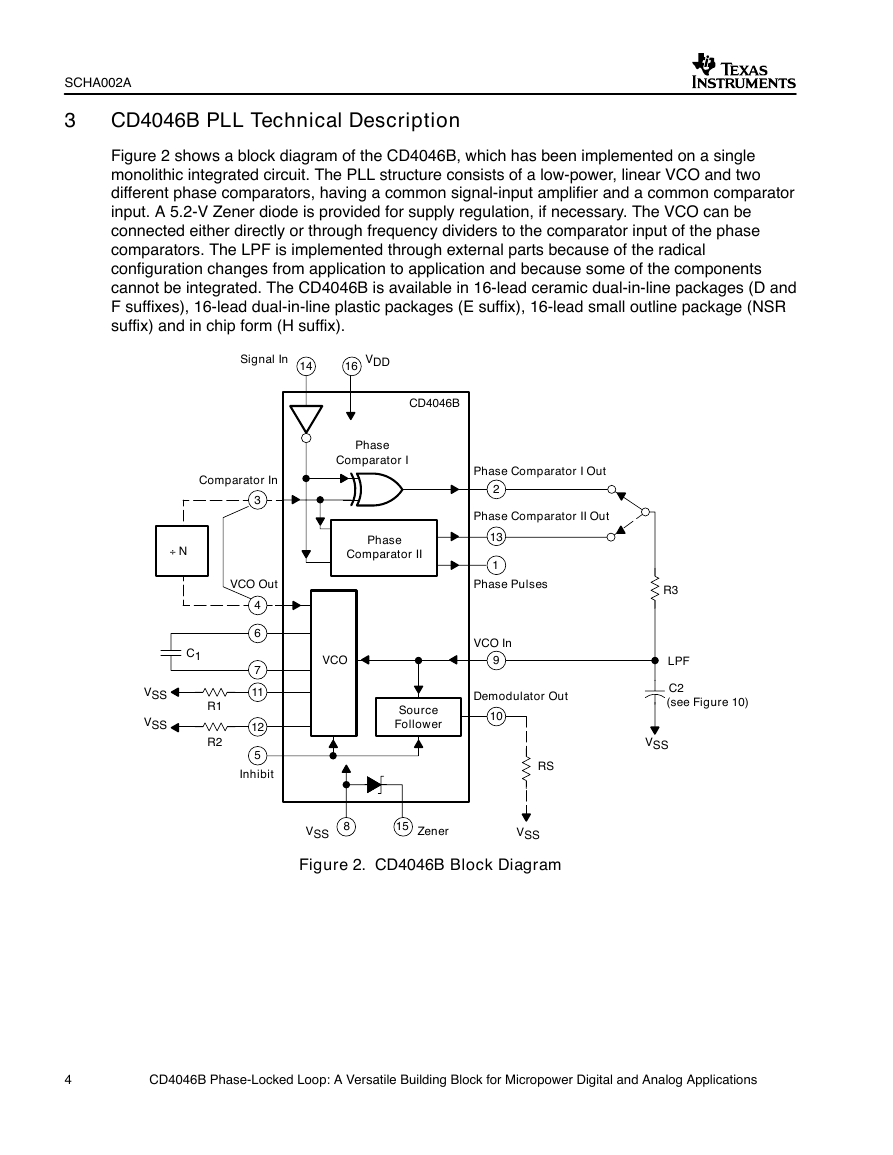
Figure 2 shows a block diagram of the CD4046B, which has been implemented on a single
monolithic integrated circuit. The PLL structure consists of a low-power, linear VCO and two
different phase comparators, having a common signal-input amplifier and a common comparator
input. A 5.2-V Zener diode is provided for supply regulation, if necessary. The VCO can be
connected either directly or through frequency dividers to the comparator input of the phase
comparators. The LPF is implemented through external parts because of the radical
configuration changes from application to application and because some of the components
cannot be integrated. The CD4046B is available in 16-lead ceramic dual-in-line packages (D and
F suffixes), 16-lead dual-in-line plastic packages (E suffix), 16-lead small outline package (NSR
suffix) and in chip form (H suffix).
Signal In
14
VDD
16
CD4046B
Phase
Comparator I
Comparator In
3
÷ N
Phase
Comparator II
Phase Comparator I Out
2
Phase Comparator II Out
13
1
Phase Pulses
VCO Out
4
6
7
11
12
5
Inhibit
C1
R1
R2
VSS
VSS
R3
LPF
C2
(see Figure 10)
VCO
VCO In
9
Demodulator Out
Source
Follower
10
VSS
RS
8
VSS
15
Zener
VSS
Figure 2. CD4046B Block Diagram
4
CD4046B Phase-Locked Loop: A Versatile Building Block for Micropower Digital and Analog Applications
�
SCHA002A
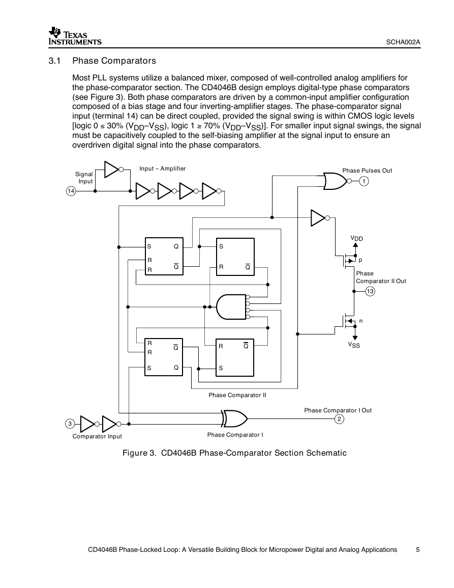
3.1 Phase Comparators
Most PLL systems utilize a balanced mixer, composed of well-controlled analog amplifiers for
the phase-comparator section. The CD4046B design employs digital-type phase comparators
(see Figure 3). Both phase comparators are driven by a common-input amplifier configuration
composed of a bias stage and four inverting-amplifier stages. The phase-comparator signal
input (terminal 14) can be direct coupled, provided the signal swing is within CMOS logic levels
[logic 0 ≤ 30% (VDD–VSS), logic 1 ≥ 70% (VDD–VSS)]. For smaller input signal swings, the signal
must be capacitively coupled to the self-biasing amplifier at the signal input to ensure an
overdriven digital signal into the phase comparators.
Input – Amplifier
Signal
Input
14
S
R
R
R
R
S
Q
Q
Q
Q
S
R
R
S
Q
Q
Phase Pulses Out
1
VDD
p
Phase
Comparator II Out
13
n
VSS
3
Comparator Input
Phase Comparator II
Phase Comparator I
Phase Comparator I Out
2
Figure 3. CD4046B Phase-Comparator Section Schematic
CD4046B Phase-Locked Loop: A Versatile Building Block for Micropower Digital and Analog Applications
5
�
SCHA002A
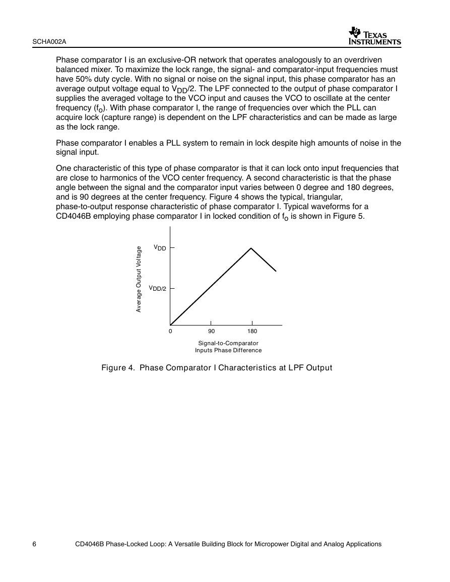
Phase comparator I is an exclusive-OR network that operates analogously to an overdriven
balanced mixer. To maximize the lock range, the signal- and comparator-input frequencies must
have 50% duty cycle. With no signal or noise on the signal input, this phase comparator has an
average output voltage equal to VDD/2. The LPF connected to the output of phase comparator I
supplies the averaged voltage to the VCO input and causes the VCO to oscillate at the center
frequency (fo). With phase comparator I, the range of frequencies over which the PLL can
acquire lock (capture range) is dependent on the LPF characteristics and can be made as large
as the lock range.
Phase comparator I enables a PLL system to remain in lock despite high amounts of noise in the
signal input.
One characteristic of this type of phase comparator is that it can lock onto input frequencies that
are close to harmonics of the VCO center frequency. A second characteristic is that the phase
angle between the signal and the comparator input varies between 0 degree and 180 degrees,
and is 90 degrees at the center frequency. Figure 4 shows the typical, triangular,
phase-to-output response characteristic of phase comparator I. Typical waveforms for a
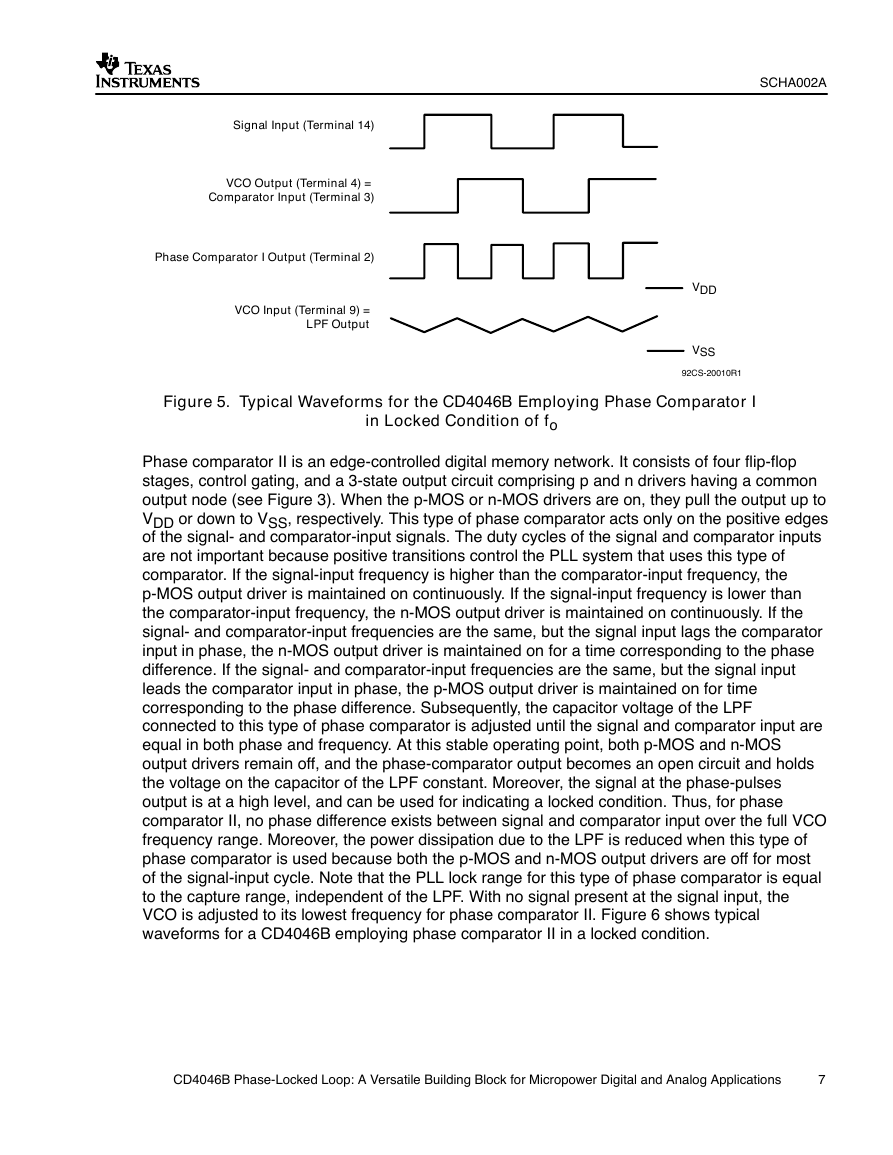
CD4046B employing phase comparator I in locked condition of fo is shown in Figure 5.
VDD
VDD/2
e
g
a
t
l
o
V
t
u
p
t
u
O
e
g
a
r
e
v
A
0
90
180
Signal-to-Comparator
Inputs Phase Difference
Figure 4. Phase Comparator I Characteristics at LPF Output
6
CD4046B Phase-Locked Loop: A Versatile Building Block for Micropower Digital and Analog Applications
�
Signal Input (Terminal 14)
VCO Output (Terminal 4) =
Comparator Input (Terminal 3)
Phase Comparator I Output (Terminal 2)
VCO Input (Terminal 9) =
LPF Output
SCHA002A
VDD
VSS
92CS-20010R1
Figure 5. Typical Waveforms for the CD4046B Employing Phase Comparator I
in Locked Condition of fo
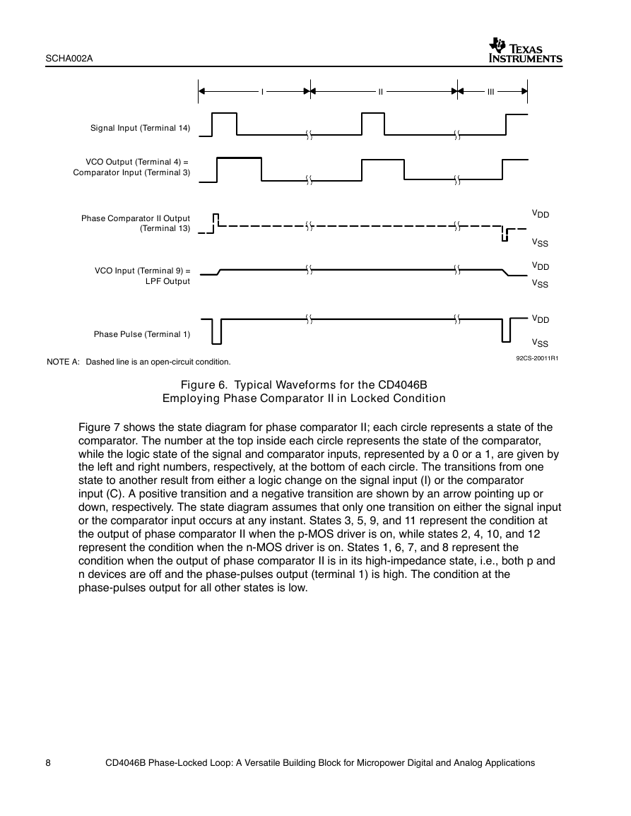
Phase comparator II is an edge-controlled digital memory network. It consists of four flip-flop
stages, control gating, and a 3-state output circuit comprising p and n drivers having a common
output node (see Figure 3). When the p-MOS or n-MOS drivers are on, they pull the output up to
VDD or down to VSS, respectively. This type of phase comparator acts only on the positive edges
of the signal- and comparator-input signals. The duty cycles of the signal and comparator inputs
are not important because positive transitions control the PLL system that uses this type of
comparator. If the signal-input frequency is higher than the comparator-input frequency, the
p-MOS output driver is maintained on continuously. If the signal-input frequency is lower than
the comparator-input frequency, the n-MOS output driver is maintained on continuously. If the
signal- and comparator-input frequencies are the same, but the signal input lags the comparator
input in phase, the n-MOS output driver is maintained on for a time corresponding to the phase
difference. If the signal- and comparator-input frequencies are the same, but the signal input
leads the comparator input in phase, the p-MOS output driver is maintained on for time
corresponding to the phase difference. Subsequently, the capacitor voltage of the LPF
connected to this type of phase comparator is adjusted until the signal and comparator input are
equal in both phase and frequency. At this stable operating point, both p-MOS and n-MOS
output drivers remain off, and the phase-comparator output becomes an open circuit and holds
the voltage on the capacitor of the LPF constant. Moreover, the signal at the phase-pulses
output is at a high level, and can be used for indicating a locked condition. Thus, for phase
comparator II, no phase difference exists between signal and comparator input over the full VCO
frequency range. Moreover, the power dissipation due to the LPF is reduced when this type of
phase comparator is used because both the p-MOS and n-MOS output drivers are off for most
of the signal-input cycle. Note that the PLL lock range for this type of phase comparator is equal
to the capture range, independent of the LPF. With no signal present at the signal input, the
VCO is adjusted to its lowest frequency for phase comparator II. Figure 6 shows typical
waveforms for a CD4046B employing phase comparator II in a locked condition.
CD4046B Phase-Locked Loop: A Versatile Building Block for Micropower Digital and Analog Applications
7
�
SCHA002A
Signal Input (Terminal 14)
VCO Output (Terminal 4) =
Comparator Input (Terminal 3)
Phase Comparator II Output
(Terminal 13)
VCO Input (Terminal 9) =
LPF Output
Phase Pulse (Terminal 1)
NOTE A: Dashed line is an open-circuit condition.
I
II
III
VDD
VSS
VDD
VSS
VDD
VSS
92CS-20011R1
Figure 6. Typical Waveforms for the CD4046B
Employing Phase Comparator II in Locked Condition
Figure 7 shows the state diagram for phase comparator II; each circle represents a state of the
comparator. The number at the top inside each circle represents the state of the comparator,
while the logic state of the signal and comparator inputs, represented by a 0 or a 1, are given by
the left and right numbers, respectively, at the bottom of each circle. The transitions from one
state to another result from either a logic change on the signal input (I) or the comparator
input (C). A positive transition and a negative transition are shown by an arrow pointing up or
down, respectively. The state diagram assumes that only one transition on either the signal input
or the comparator input occurs at any instant. States 3, 5, 9, and 11 represent the condition at
the output of phase comparator II when the p-MOS driver is on, while states 2, 4, 10, and 12
represent the condition when the n-MOS driver is on. States 1, 6, 7, and 8 represent the
condition when the output of phase comparator II is in its high-impedance state, i.e., both p and
n devices are off and the phase-pulses output (terminal 1) is high. The condition at the
phase-pulses output for all other states is low.
8
CD4046B Phase-Locked Loop: A Versatile Building Block for Micropower Digital and Analog Applications
�


 2023年江西萍乡中考道德与法治真题及答案.doc
 2012年重庆南川中考生物真题及答案.doc
 2013年江西师范大学地理学综合及文艺理论基础考研真题.doc
 2020年四川甘孜小升初语文真题及答案I卷.doc
 2020年注册岩土工程师专业基础考试真题及答案.doc
 2023-2024学年福建省厦门市九年级上学期数学月考试题及答案.doc
 2021-2022学年辽宁省沈阳市大东区九年级上学期语文期末试题及答案.doc
 2022-2023学年北京东城区初三第一学期物理期末试卷及答案.doc
 2018上半年江西教师资格初中地理学科知识与教学能力真题及答案.doc
 2012年河北国家公务员申论考试真题及答案-省级.doc
 2020-2021学年江苏省扬州市江都区邵樊片九年级上学期数学第一次质量检测试题及答案.doc
 2022下半年黑龙江教师资格证中学综合素质真题及答案.doc