《硅超大规模集成电路工艺技术——理论、实践与模型》(英文版)�
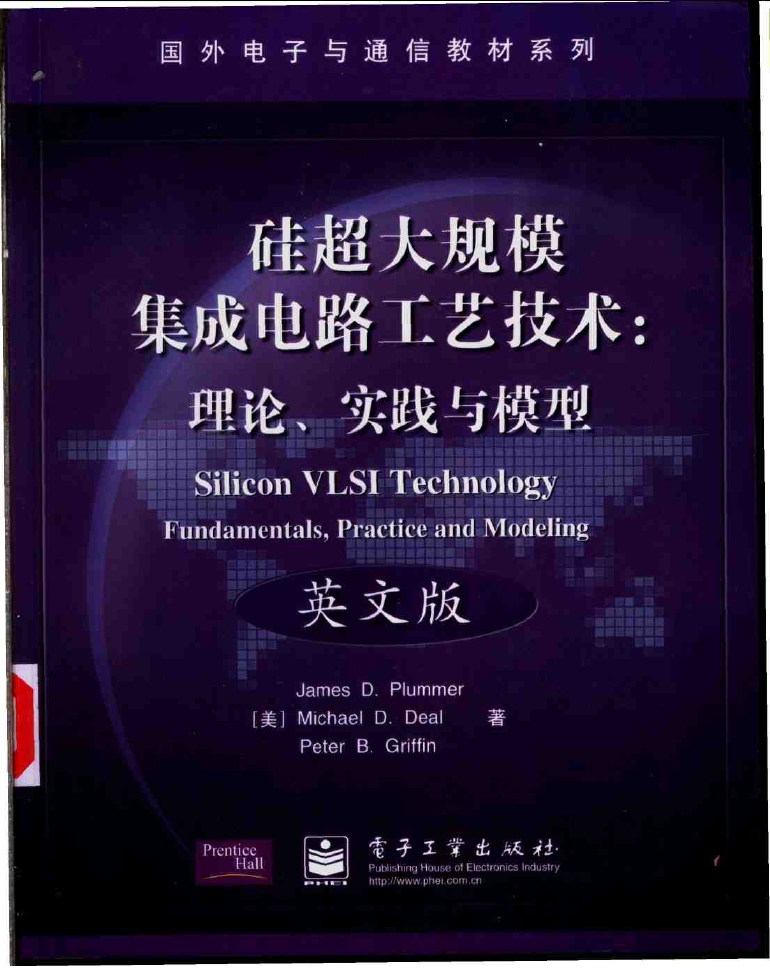
封面1�
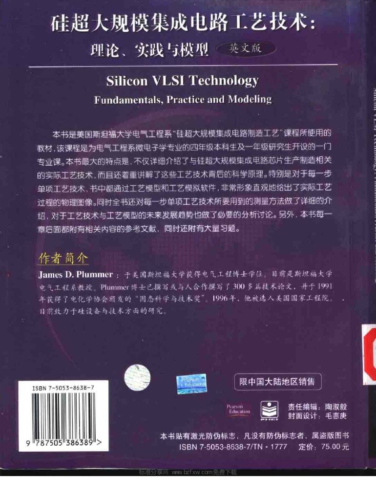
底面�
封面2�
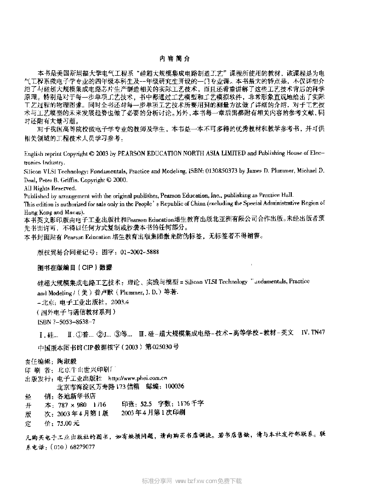
内容简介�
序
出版说明
教材出版委员会
前言(英文)
目录概览
目录(英文)
正文�
Chapter 1 lntroduction and Histerial Perspective �
1.1 Introduction �
1.2 Integrated Circuits and the Planar Process--Key Inventions That Made It All Possible �
1.3 Semiconductors �
1.4 Semiconductor Devices �
1.4.1 PN Diodes �
1.4.2 MOS Transistors �
1.4.3 Bipolar Junction Transistors �
1.5 Semiconductor Technology Families �
1.6 Modern Scientific Discovery-Experiments Theory, and Computer Simulation �
1.7 The Plan For This Book �
1.8 Summary of Key Ideas �
1.9 References �
1.10 Problems �
Chapter 2 Modem CMOS Technology �
2.1 Introduction �
2.2 CMOS Profess Flow �
2.2.1 The Beginning-Choosing a Substrate �
2.2.2 Active Region Formation �
2.2.3 Process Option for Device Isolation-Shallow Trench Isolation �
2.2.4 N and P Well Formation �
2.2.5 Process Options for Active Region and Well Formation �
2.2.6 Gate Formation. �
2.2.7 Tip or Extension (LDD) Formation �
2.2.8 Source/Drain Formation �
2.2.9 Contact and Local Interconnect Formation �
2.2.10 Multilevel Metal Formation �
2.3 Summary of Key Ideas �
2.4 Problems �
Chapter 3 Crystal Growth, Wafer Fabrication and Basic Properties of Silicon Wafers �
3.1 Introduction �
3.2 Historical Development and Basic Concepts �
3.2.1 Crystal Structure �
3.2.2 Defects in Crystals �
3.2.3 Raw Materials and Purification �
3.2.4 Czochralski and Float-Zone Crystal Growth Methods �
3.2.5 Wafer Preparation and Specification �
3.3 Manufacturing Methods and Equipment �
3.4 Measurement Methods �
3.4.1 Electrical Measurements �
3.4.1.1 Hot Point Probe �
3.4.1.2 Sheet Resistance �
3.4.1.3 Hall Effect Measurements �
3.4.2 Physical Measurements �
3.4.2.1 Defect Etches �
3.4.2.2 Fourier Transform Infrared Spectroscopy (FTIR) �
3.4.2.3 Electron Microscopy �
3.5 Models and Simulation �
3.5.1 Czochralski Crystal Growth �
3.5.2 Dopant Incorporation during CZ Crystal Growth �
3.5.3 Zone Refining and FZ Growth �
3.5.4 Point Defects �
3.5.5 Oxygen in Silicon �
3.5.6 Carbon in Silicon �
3.5.7 Simulation �
3.6 Limits and Future Trends in Technologies and Models �
3.7 Summary of Key Ideas �
3.8 References �
3.9 Problems �
Chapter 4 Semiconductor Manufacturing--Clean Rooms Wafer Cleaning and Gettering �
4.1 Introduction �
4.2 Historical Development and Basic Concepts �
4.2.1 Level l Contamination Reduction: Clean Factories �
4.2.2 Level 2 Contamination Reduction: Wafer Cleaning �
4.2.3 Level 3 Contamination Reduction: Gettering �
4.3 Manufacturing Methods and Equipment �
4.3.1 Level 1 Contamination Reduction: Clean Factories �
4.3.2 Level 2 Contamination Reduction: Wafer Cleaning �
4.3.3 Level 3 Contamination Reduction: Gettering. �
4.4 Measurement Methods �
4.4.1 Level 1 Contamination Reduction: Clean Factories �
4.4.2 Level 2 Contamination Reduction: Wafer Cleaning �
4.4.3 Level 3 Contamination Reduction: Gettering �
4.5 Models and Simulation �
4.5.1 Level 1 Contamination Reduction: Clean Factories �
4.5.2 Level 2 Contamination Reduction: Wafer Cleaning �
4.5.3 Level 3 Contamination Reduction: Gettering �
4.5.3.1 Step 1: Making the Metal Atoms Mobile �
4.5.3.2 Step 2: Metal Diffusion to the Gettering Site �
4.5.3.3 Step 3: Trapping the Metal Atoms at tbe Gettering Site �
4.6 Limits and Future Trends in Technologies and Models �
4.7 Summary of Key Ideas �
4.8 References �
4.9 Problems �
Chapter 5 Lithography �
5.1 Introduction �
5.2 Historical Development and Basic Concepts �
5.2.1 Light Sources �
5.2.2 Wafer Exposure Systems �
5.2.2.1 Optics Basics-Ray Tracing and Diffraction �
5.2.2.2 Projection Systems (Fraunhofer Diffraction) �
5.2.2.3 Contact and Proximity Systems (Fresnel Diffraction) �
5.2.3 Photoresists �
5.2.3.1 g-line and i-line Resists �
5.2.3.2 Deep Ultraviolet (DUV) Resists �
5.2.3.3 Basic Properties and Characterization of Resists �
5.2.4 Mask Engineering-Optical Proximity Correction and Phase Shifting �
5.3 Manufacturing Methods and Equipment �
5.3.1 Wafer Exposure Systems �
5.3.2 Photoresists �
5.4 Measurement Methods �
5.4.1 Measurement of Mask Features and Defects �
5.4.2 Measurement of Resist Patterns �
5.4.3 Measurement of Etched Features �
5.5 Models and Simulation �
5.5.1 Wafer Exposure Systems �
5.5.2 Optical Intensity Pattern in the Photoresist �
5.5.3 Photoresist Exposure �
5.5.3.1 g-line and i-line DNQ Resists �
5.5.3.2 DUV Resists �
5.5.4 Postexposure Bake (PEB) �
5.5.4.1 g-line and i-line DNQ Resists �
5.5.4.2 DUV Resists �
5.5.5 Photoresist Developing �
5.5.6 Photoresist Postbake �
5.5.7 Advanced Mask Engineering �
5.6 Limits and Future Trends in Technologies and Models �
5.6.1 Electron Beam Lithography �
5.6.2 X-ray Lithography �
5.6.3 Advanced Mask Engineering �
5.6.4 New Resists �
5.7 Summary of Key Ideas �
5.8 References �
5.9 Problems �
Chapter 6 Thermal Oxidation and the Si/SiO2 Interface �
6.1 Introduction �
6.2 Historical Development and Basic Concepts �
6.3 Manufacturing Methods and Equipment �
6.4 Measurement Methods �
6.4.1 Physical Measurements �
6.4.2 Optical Measurements �
6.4.3 Electrical Measurements-The MOS Capacitor �
6.5 Models and Simulation �
6.5.1 First-Order Planar Growth Kinetic -The Linear Parabolic Model �
6.5.2 Other Models for Planar Oxidation Kinetics �
6.5.3 Thin Oxide SiO2 Growth Kinetics �
6.5.4 Dependence of Growth Kinetics on Pressure �
6.5.5 Dependence of Growth Kinetics on Crystal Orientation �
6.5.6 Mixed Ambient Growth Kinetics �
6.5.7 2D SiO2 Growth Kinetics �
6.5.8 Advanced Point Defect Based Models for Oxidation �
6.5.9 Substrate Doping Effects �
6.5.10 Polysilicon Oxidation �
6.5.11 Si3N4 Growth and Oxidation Kinetics �
6.5.12 Silicide Oxidation �
6.5.13 Si/SiO2 Interface Charges �
6.5.14 Complete Oxidation Module Simulation �
6.6 Limits and Future Trends in Technologies and Models �
6.7 Summary of Key Ideas �
6.8 References �
6.9 Problems �
Chapter 7 Dopant Diffusion �
7.1 Introduction �
7.2 Historical Development and Basic Concepts �
7.2.1 Dopant Solid Solubility �
7.2.2 Diffusion from a Macroscopic Viewpoint �
7.2.3 Analytic Solutions of the Diffusion Equation �
7.2.4 Gaussian Solution in an Infinite Medium �
7.2.5 Gaussian Solution Near a Surface �
7.2.6 Error-Function Solution in an Infinite Medium �
7.2.7 Error-Function Solution Near a Surface �
7.2.8 Intrinsic Diffusion Coefficients of Dopants in Silicon �
7.2.9 Effect of Successive Diffusion Steps �
7.2.10 Design and Evaluation of Diffused Layers �
7.2.11 Summary of Basic Diffusion Concepts �
7.3 Manufacturing Methods and Equipment �
7.4 Measurement Methods �
7.4.1 SIMS �
7.4.2 Spreading Resistance �
7.4.3 Sheet Resistance �
7.4.4 Capacitance Voltage �
7.4.5 TEM Cross Section �
7.4.6 2D Electrical Measurements Using Scanning Probe Microscopy �
7.4.7 Inverse Electrical Easements �
7.5 Models and Simulation �
7.5.1 Numerical Solutions of the Diffusion Equation �
7.5.2 Modifications to Fick's Laws to Account for Electric Field Effects �
7.5.3 Modifications to Fick's Laws to Account for Concentration-Dependent Diffusion �
7.5.4 Segregation �
7.5.5 Interfacial Dopant Pileup �
7.5.6 Summary of the Macroscopic Diffusion Approach �
7.5.7 Tbe Physical Basis for Diffusion at an Atomic Scale �
7.5.8 Oxidation-Enhanced or -Retarded Diffusion �
7.5.9 Dopant Diffusion Occurs by Both I and V �
7.5.10 Activation Energy for Self-Diffusion and Dopant Diffusion �
7.5.11 Dopant-Defect Interactions �
7.5.12 Chemical Equilibrium Formulation for Dopant-Defect Interactions �
7.5.13 Simplified Expression for Modeling �
7.5.14 Charge State Effects �
7.6 Limits and Future Trends in Technologies and Models �
7.6.1 Doping Methods �
7.6.2 Advanced Dopant Profile Modeling-Fully Kinetic Description of Dopant-Defect Interactions �
7.7 Summary of Key Ideas �
7.8 References �
7.9 Problems �
Chapter 8 lon Implantation �
8.1 Introduction �
8.2 Historical Development and Basic Concepts �
8.2.1 Implants in Real Silicon-The Role of the Crystal Structure �
8.3 Manufacturing Methods and Equipment �
8.3.1 High-Energy Implants �
8.3.2 Ultralow Energy Implants �
8.3.3 lon Beam Heating �
8.4 Measurement Methods �
8.5 Models and Simulations �
8.5.1 Nuclear Stopping �
8.5.2 Nonlocal Electronic Stopping �
8.5.3 Local Electronic Stopping �
8.5.4 Total Stopping Powers �
8.5.5 Damage Production �
8.5.6 Damage Annealing �
8.5.7 Solid-Phase Epitaxy �
8.5.8 Dopant Activation �
8.5.9 Transient-Enhanced Diffusion �
8.5.1O Atomic-Level Understanding of TED �
8.5.11 Effects on Devices �
8.6 Limits and Future Trends in Technologies and Models �
8.7 Summary of Key Ideas �
8.8 References �
8.9 Problems �
Chapter 9 Thin Film Deposition �
9.1 Introduction �
9.2 Historical Development and Basic Concepts �
9.2.1 Chemical Vapor Deposition (CVD) �
9.2.1.1 Atmospheric Pressure Chemical Vapor Deposition (APCVD) �
9.2.1.2 Low-Pressure Chemical Vapor Deposition (LPCVD) �
9.2.1.3 Plasma-Enhanced Chemical Vapor Deposition (PECVD) �
9.2.1.4 High-Density Plasma Chemical Vapor Deposition (HDPCVD) �
9.2.2 Physical Vapor Deposition (PVD) �
9.2.2.1 Evaporation �
9.2.2.2 Sputter Deposition �
9.3 Manufacturing Methods �
9.3.1 Epitaxial Silicon Deposition �
9.3.2 Polycrystalline Silicon Deposition �
9.3.3 Silicon Nitride Deposition �
9.3.4 Silicon Dioxide Deposition �
9.3.5 A1 Deposition �
9.3.6 Ti and Ti-W Deposition �
9.3.7 W Deposition �
9.3.8 TiSi2 and WSi2 Deposition �
9.3.9 TiN Deposition �
9.3.10 Cu Deposition �
9.4 Measurement Methods �
9.5 Models and Simulation �
9.5.1 Models for Deposition Simulations �
9.5.1.1 Models in Physically Based Simulators Such as SPEEDIE �
9.5.1.2 Models for Different Types of Deposition Systems �
9.5.1.3 Comparing CVD and PVD and Typical Parameter Values �
9.5.2 Simulations of Deposition Using a Physically Based Simulator, SPEEDIE �
9.5.3 Other Deposition Simulations �
9.6 Limits and Future Trends in Technologies and Models �
9.7 Summary of Key Ideas �
9.8 References �
9.9 Problems �
Chapter le Etching �
10.1 Introduction �
10.2 Historical Development and Basic Concepts �
10.2.1 Wet Etching �
10.2.2 Plasma Etching �
10.2.2.1 Plasma Etching Mechanisms �
10.2.2.2 Types of Plasma Etch Systems �
10.2.2.3 Summary of Plasma Systems and Mechanisms �
10.3 Manufacturing Methods �
10.3.1 Plasma Etching Conditions and Issues �
10.3.2 Plasma Etch Methods for Various Films �
10.3.2.1 Plasma Etching Silicon Dioxide �
10.3.2.2 Plasma Etching Polysilicon �
10.3.2.3 Plasma Etching Aluminum �
10.4 Measurement Methods. �
10.5 Models and Simulation. �
10.5.1 Models for Etching Simulation �
10.5.2 Etching Models----Linear Etch Model �
10.5.3 Etching Models----Saturation/Adsorption Model for lon-Embanked Etching �
10.5.4 Etching Models----More Advanced Models �
10.5.5 Other Etching Simulation �
10.6 Limits and Future Trends in Technologies and Models �
10.7 Summary of Key Ideas �
10.8 References �
10.9 Problems �
Chapter 11 Back-End Technology �
11.1 Introduction �
11.2 Historical Development and Basic Concepts �
11.2.1 Contacts �
11.2.2 Interconnects and Vias �
11.2.3 Dielectrics �
11.3 Manufacturing Methods and Equipment �
11.3.1 Silicided Gates and Source/Drain Regions �
11.3.2 First-level Dielectric Processing �
11.3.3 Contact Formation �
11.3.4 Global Interconnects �
11.3.5 IMD Deposition and Planarization �
11.3.6 Via Formation �
11.3.7 Final Steps �
11.4 Measurement Methods �
11.4.1 Morphological Measurements �
11.4.2 Electrical Measurements �
11.4.3 Chemical and Structural Measurements �
11.4.4 Mechanical Measurements �
11.5 Models and Simulation �
11.5.1 Silicide Formation �
11.5.2 Chemical-Mechanical Polishing �
11.5.3 Reflow �
11.5.4 Grain Growth �
11.5.5 Diffusion in Polycrystalline Materials �
11.5.6 Electromigration �
11.6 Limits and Future Trends in Technologies and Models �
11.7 Summary of Key Ideas �
11.8 References �
11.9 Problems �
Appendices �
A.1 Standard Prefixes �
A.2 Useful Conversions �
A.3 Physical Constants �
A.4 Physical Properties of Silicon �
A.5 Properties of Insulators Used in Silicon Technology �
A.6 Color Chart for Deposited Si3N4 Films Observed Perpendicularly under Daylight Fluorescent Lighting �
A.7 color Chart for Thermally Grown SiO2 Films Observed Perpendicularly under Daylight Fluorescent Lighting �
A.8 Irwin Curves �
A.9 Error Function �
A.10 List of Important Symbols �
A.11 List of Common Acronyms �
A.12 Tables in Text �
A.13 Answers to Selected Problems �
Index�
退出阅读系统�


 2023年江西萍乡中考道德与法治真题及答案.doc
 2012年重庆南川中考生物真题及答案.doc
 2013年江西师范大学地理学综合及文艺理论基础考研真题.doc
 2020年四川甘孜小升初语文真题及答案I卷.doc
 2020年注册岩土工程师专业基础考试真题及答案.doc
 2023-2024学年福建省厦门市九年级上学期数学月考试题及答案.doc
 2021-2022学年辽宁省沈阳市大东区九年级上学期语文期末试题及答案.doc
 2022-2023学年北京东城区初三第一学期物理期末试卷及答案.doc
 2018上半年江西教师资格初中地理学科知识与教学能力真题及答案.doc
 2012年河北国家公务员申论考试真题及答案-省级.doc
 2020-2021学年江苏省扬州市江都区邵樊片九年级上学期数学第一次质量检测试题及答案.doc
 2022下半年黑龙江教师资格证中学综合素质真题及答案.doc