TMS320LF2407A, TMS320LF2406A, TMS320LF2403A, TMS320LF2402A
TMS320LC2406A, TMS320LC2404A, TMS320LC2402A
DSP CONTROLLERS
SPRS145H – JULY 2000 – REVISED OCTOBER 2002
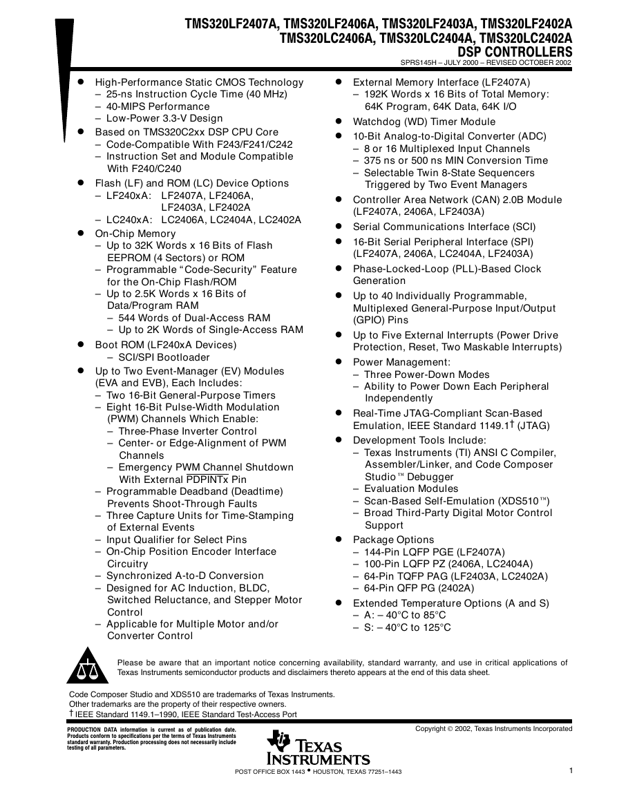
D High-Performance Static CMOS Technology
D External Memory Interface (LF2407A)
– 25-ns Instruction Cycle Time (40 MHz)
– 40-MIPS Performance
– Low-Power 3.3-V Design
D Based on TMS320C2xx DSP CPU Core
– Code-Compatible With F243/F241/C242
– Instruction Set and Module Compatible
With F240/C240
D Flash (LF) and ROM (LC) Device Options
– LF240xA: LF2407A, LF2406A,
LF2403A, LF2402A
– LC240xA: LC2406A, LC2404A, LC2402A
D On-Chip Memory
– Up to 32K Words x 16 Bits of Flash
EEPROM (4 Sectors) or ROM
– Programmable “Code-Security” Feature
for the On-Chip Flash/ROM
– Up to 2.5K Words x 16 Bits of
Data/Program RAM
– 544 Words of Dual-Access RAM
– Up to 2K Words of Single-Access RAM
D Boot ROM (LF240xA Devices)
– SCI/SPI Bootloader
D Up to Two Event-Manager (EV) Modules
(EVA and EVB), Each Includes:
– Two 16-Bit General-Purpose Timers
– Eight 16-Bit Pulse-Width Modulation
(PWM) Channels Which Enable:
– Three-Phase Inverter Control
– Center- or Edge-Alignment of PWM
Channels
– Emergency PWM Channel Shutdown
With External PDPINTx Pin
– Programmable Deadband (Deadtime)
Prevents Shoot-Through Faults
– Three Capture Units for Time-Stamping
of External Events
– Input Qualifier for Select Pins
– On-Chip Position Encoder Interface
Circuitry
– Synchronized A-to-D Conversion
– Designed for AC Induction, BLDC,
Switched Reluctance, and Stepper Motor
Control
– Applicable for Multiple Motor and/or
Converter Control
– 192K Words x 16 Bits of Total Memory:
64K Program, 64K Data, 64K I/O
D Watchdog (WD) Timer Module
D 10-Bit Analog-to-Digital Converter (ADC)
– 8 or 16 Multiplexed Input Channels
– 375 ns or 500 ns MIN Conversion Time
– Selectable Twin 8-State Sequencers
Triggered by Two Event Managers
D Controller Area Network (CAN) 2.0B Module
(LF2407A, 2406A, LF2403A)
D Serial Communications Interface (SCI)
D 16-Bit Serial Peripheral Interface (SPI)
(LF2407A, 2406A, LC2404A, LF2403A)
D Phase-Locked-Loop (PLL)-Based Clock
Generation
D Up to 40 Individually Programmable,
Multiplexed General-Purpose Input/Output
(GPIO) Pins
D Up to Five External Interrupts (Power Drive
Protection, Reset, Two Maskable Interrupts)
D Power Management:
– Three Power-Down Modes
– Ability to Power Down Each Peripheral
Independently
D Real-Time JTAG-Compliant Scan-Based
Emulation, IEEE Standard 1149.1† (JTAG)
D Development Tools Include:
– Texas Instruments (TI) ANSI C Compiler,
Assembler/Linker, and Code Composer
Studio Debugger
– Evaluation Modules
– Scan-Based Self-Emulation (XDS510)
– Broad Third-Party Digital Motor Control
Support
D Package Options
– 144-Pin LQFP PGE (LF2407A)
– 100-Pin LQFP PZ (2406A, LC2404A)
– 64-Pin TQFP PAG (LF2403A, LC2402A)
– 64-Pin QFP PG (2402A)
D Extended Temperature Options (A and S)
– A: – 40°C to 85°C
– S: – 40°C to 125°C
Please be aware that an important notice concerning availability, standard warranty, and use in critical applications of
Texas Instruments semiconductor products and disclaimers thereto appears at the end of this data sheet.
Code Composer Studio and XDS510 are trademarks of Texas Instruments.
Other trademarks are the property of their respective owners.
† IEEE Standard 1149.1–1990, IEEE Standard Test-Access Port
information
PRODUCTION DATA
is current as of publication date.
Products conform to specifications per the terms of Texas Instruments
standard warranty. Production processing does not necessarily include
testing of all parameters.
Copyright 2002, Texas Instruments Incorporated
POST OFFICE BOX 1443 • HOUSTON, TEXAS 77251–1443
1
�
TMS320LF2407A, TMS320LF2406A, TMS320LF2403A, TMS320LF2402A
TMS320LC2406A, TMS320LC2404A, TMS320LC2402A
DSP CONTROLLERS
SPRS145H – JULY 2000 – REVISED OCTOBER 2002
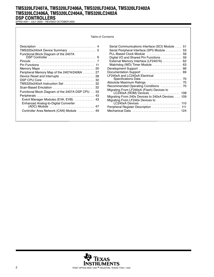
Table of Contents
4
5
Description
TMS320x240xA Device Summary
Functional Block Diagram of the 2407A
. . . . . . . . . . . . . . . . . . . . . . . . . . . . . . . . . . . . .
. . . . . . . . . . . . . . . . .
DSP Controller
Pinouts
Pin Functions
Memory Maps
Peripheral Memory Map of the 2407A/2406A
Device Reset and Interrupts
DSP CPU Core
TMS320x240xA Instruction Set
Scan-Based Emulation
Functional Block Diagram of the 2407A DSP CPU
Peripherals
. . . . . . . . . . . . . . . . . . . . . . . . . . . . . .
. . . . . . . . . . . . . . . . . . . . . . . . . . . . . . . . . . . . . . . .
. . . . . . . . . . . . . . . . . . . . . . . . . . . . . . . . . .
. . . . . . . . . . . . . . . . . . . . . . . . . . . . . . . . .
. . . . . . .
. . . . . . . . . . . . . . . . . . . . .
. . . . . . . . . . . . . . . . . . . . . . . . . . . . . . . .
. . . . . . . . . . . . . . . . . . .
. . . . . . . . . . . . . . . . . . . . . . . . . .
. .
. . . . . . . . . . . . . . . . . . . . . . . . . . . . . . . . . . . .
. . . . . . . . . . . .
Event Manager Modules (EVA, EVB)
Enhanced Analog-to-Digital Converter
6
7
11
20
27
28
32
32
32
33
43
43
(ADC) Module
Controller Area Network (CAN) Module
. . . . . . . . . . . . . . . . . . . . . . . . . . . .
. . . . . . . . . .
47
49
Serial Communications Interface (SCI) Module
Serial Peripheral Interface (SPI) Module
PLL-Based Clock Module
Digital I/O and Shared Pin Functions
External Memory Interface (LF2407A)
Watchdog (WD) Timer Module
. . . .
. . . . . . . . . .
. . . . . . . . . . . . . . . . . . . . . .
. . . . . . . . . . . . .
. . . . . . . . . . . .
. . . . . . . . . . . . . . . . . .
. . . . . . . . . . . . . . . . . . . . . . . . . . .
. . . . . . . . . . . . . . . . . . . . . . . . .
Development Support
Documentation Support
LF240xA and LC240xA Electrical
Specifications Data
Absolute Maximum Ratings
Recommended Operating Conditions
Migrating From LF240xA (Flash) Devices to
. . . . . . . . . . . . . . . . . . . . . . . . .
. . . . . . . . . . . . . . . . . . . . . .
. . . . . . . . . . . . .
51
53
56
59
62
63
66
69
70
70
70
108
109
110
111
124
LC240xA (ROM) Devices
. . . . . . . . . . . . . . . . . . .
. . .
Migrating From 240x Devices to 240xA Devices
Migrating From LF240x Devices to
LC240xA Devices
Peripheral Register Description
Mechanical Data
. . . . . . . . . . . . . . . . . . . . . . . . .
. . . . . . . . . . . . . . . . . .
. . . . . . . . . . . . . . . . . . . . . . . . . . . . . .
2
POST OFFICE BOX 1443 • HOUSTON, TEXAS 77251–1443
�
TMS320LF2407A, TMS320LF2406A, TMS320LF2403A, TMS320LF2402A
TMS320LC2406A, TMS320LC2404A, TMS320LC2402A
DSP CONTROLLERS
SPRS145H – JULY 2000 – REVISED OCTOBER 2002
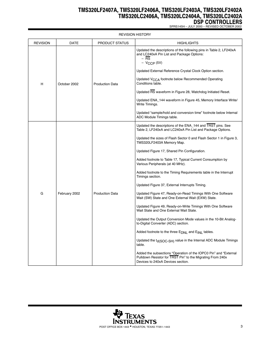
REVISION HISTORY
REVISION
DATE
PRODUCT STATUS
HIGHLIGHTS
H
October 2002
Production Data
G
February 2002
Production Data
Updated the descriptions of the following pins in Table 2, LF240xA
and LC240xA Pin List and Package Options:
– RS
– VCCP (5V)
Updated External Reference Crystal Clock Option section.
Updated VCCA footnote below Recommended Operating
Conditions table.
Updated RS waveform in Figure 28, Watchdog Initiated Reset.
Updated ENA_144 waveform in Figure 45, Memory Interface Write/
Write Timings.
Updated “sample/hold and conversion time” footnote below Internal
ADC Module Timings table.
Updated the descriptions of the ENA_144 and TRST pins. See
Table 2, LF240xA and LC240xA Pin List and Package Options.
Updated the sizes of Flash Sector 0 and Flash Sector 1 in Figure 3,
TMS320LF2403A Memory Map.
Updated Figure 17, Shared Pin Configuration.
Added footnote to Table 17, Typical Current Consumption by
Various Peripherals (at 40 MHz).
Added footnote to the Timing Requirements table in the Interrupt
Timings section.
Updated Figure 37, External Interrupts Timing.
Updated Figure 47, Ready-on-Read Timings With One Software
Wait (SW) State and One External Wait (EXW) State.
Updated Figure 49, Ready-on-Write Timings With One Software
Wait State and One External Wait State.
Updated the Output Conversion Mode values in the 10-Bit Analog-
to-Digital Converter (ADC) section.
Added footnote to the three EDNL and EINL tables.
Updated the td(SOC-SH) value in the Internal ADC Module Timings
table.
Added the subsections “Operation of the IOPC0 Pin” and “External
Pulldown Resistor for TRST Pin” to the Migrating From 240x
Devices to 240xA Devices section.
POST OFFICE BOX 1443 • HOUSTON, TEXAS 77251–1443
3
�
TMS320LF2407A, TMS320LF2406A, TMS320LF2403A, TMS320LF2402A
TMS320LC2406A, TMS320LC2404A, TMS320LC2402A
DSP CONTROLLERS
SPRS145H – JULY 2000 – REVISED OCTOBER 2002
description
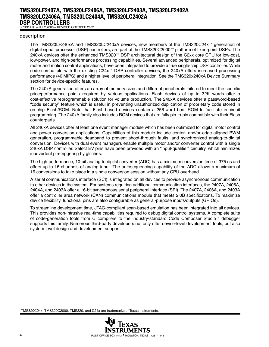
The TMS320LF240xA and TMS320LC240xA devices, new members of the TMS320C24x generation of
digital signal processor (DSP) controllers, are part of the TMS320C2000 platform of fixed-point DSPs. The
240xA devices offer the enhanced TMS320 DSP architectural design of the C2xx core CPU for low-cost,
low-power, and high-performance processing capabilities. Several advanced peripherals, optimized for digital
motor and motion control applications, have been integrated to provide a true single-chip DSP controller. While
code-compatible with the existing C24x DSP controller devices, the 240xA offers increased processing
performance (40 MIPS) and a higher level of peripheral integration. See the TMS320x240xA Device Summary
section for device-specific features.
The 240xA generation offers an array of memory sizes and different peripherals tailored to meet the specific
price/performance points required by various applications. Flash devices of up to 32K words offer a
cost-effective reprogrammable solution for volume production. The 240xA devices offer a password-based
“code security” feature which is useful in preventing unauthorized duplication of proprietary code stored in
on-chip Flash/ROM. Note that Flash-based devices contain a 256-word boot ROM to facilitate in-circuit
programming. The 240xA family also includes ROM devices that are fully pin-to-pin compatible with their Flash
counterparts.
All 240xA devices offer at least one event manager module which has been optimized for digital motor control
and power conversion applications. Capabilities of this module include center- and/or edge-aligned PWM
generation, programmable deadband to prevent shoot-through faults, and synchronized analog-to-digital
conversion. Devices with dual event managers enable multiple motor and/or converter control with a single
240xA DSP controller. Select EV pins have been provided with an “input-qualifier” circuitry, which minimizes
inadvertent pin-triggering by glitches.
The high-performance, 10-bit analog-to-digital converter (ADC) has a minimum conversion time of 375 ns and
offers up to 16 channels of analog input. The autosequencing capability of the ADC allows a maximum of
16 conversions to take place in a single conversion session without any CPU overhead.
A serial communications interface (SCI) is integrated on all devices to provide asynchronous communication
to other devices in the system. For systems requiring additional communication interfaces, the 2407A, 2406A,
2404A, and 2403A offer a 16-bit synchronous serial peripheral interface (SPI). The 2407A, 2406A, and 2403A
offer a controller area network (CAN) communications module that meets 2.0B specifications. To maximize
device flexibility, functional pins are also configurable as general-purpose inputs/outputs (GPIOs).
To streamline development time, JTAG-compliant scan-based emulation has been integrated into all devices.
This provides non-intrusive real-time capabilities required to debug digital control systems. A complete suite
of code-generation tools from C compilers to the industry-standard Code Composer Studio debugger
supports this family. Numerous third-party developers not only offer device-level development tools, but also
system-level design and development support.
TMS320C24x, TMS320C2000, TMS320, and C24x are trademarks of Texas Instruments.
4
POST OFFICE BOX 1443 • HOUSTON, TEXAS 77251–1443
�
TMS320LF2407A, TMS320LF2406A, TMS320LF2403A, TMS320LF2402A
TMS320LC2406A, TMS320LC2404A, TMS320LC2402A
DSP CONTROLLERS
SPRS145H – JULY 2000 – REVISED OCTOBER 2002
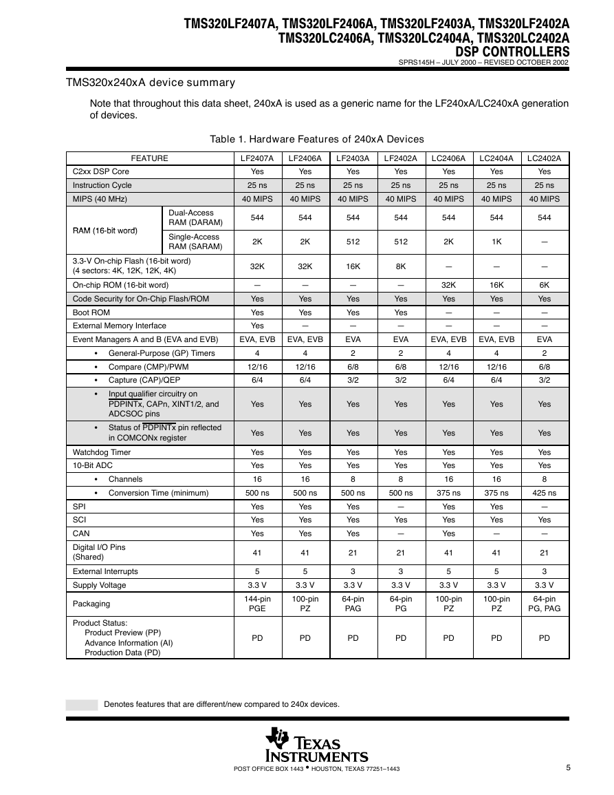
TMS320x240xA device summary
Note that throughout this data sheet, 240xA is used as a generic name for the LF240xA/LC240xA generation
of devices.
Table 1. Hardware Features of 240xA Devices
FEATURE
LF2407A
LF2406A
LF2403A
LF2402A
LC2406A
LC2404A
LC2402A
C2xx DSP Core
Instruction Cycle
MIPS (40 MHz)
RAM (16 bit ord)
RAM (16-bit word)
Dual-Access
RAM (DARAM)
Single-Access
RAM (SARAM)
3.3-V On-chip Flash (16-bit word)
(4 sectors: 4K, 12K, 12K, 4K)
On-chip ROM (16-bit word)
Code Security for On-Chip Flash/ROM
Boot ROM
External Memory Interface
Event Managers A and B (EVA and EVB)
S General-Purpose (GP) Timers
S Compare (CMP)/PWM
S Capture (CAP)/QEP
S
S
Input qualifier circuitry on
PDPINTx, CAPn, XINT1/2, and
ADCSOC pins
Status of PDPINTx pin reflected
in COMCONx register
Watchdog Timer
10-Bit ADC
S Channels
S Conversion Time (minimum)
SPI
SCI
CAN
Digital I/O Pins
(Shared)
External Interrupts
Supply Voltage
Packaging
Product Status:
Product Preview (PP)
Advance Information (AI)
Production Data (PD)
Yes
25 ns
Yes
25 ns
Yes
25 ns
Yes
25 ns
Yes
25 ns
Yes
25 ns
Yes
25 ns
40 MIPS
40 MIPS
40 MIPS
40 MIPS
40 MIPS
40 MIPS
40 MIPS
544
2K
32K
—
Yes
Yes
Yes
544
2K
32K
—
Yes
Yes
—
EVA, EVB
EVA, EVB
4
12/16
6/4
Yes
Yes
Yes
Yes
16
4
12/16
6/4
Yes
Yes
Yes
Yes
16
544
512
16K
—
Yes
Yes
—
EVA
2
6/8
3/2
Yes
Yes
Yes
Yes
8
544
512
8K
—
Yes
Yes
—
EVA
2
6/8
3/2
Yes
Yes
Yes
Yes
8
544
2K
—
32K
Yes
—
—
544
1K
—
16K
Yes
—
—
EVA, EVB
EVA, EVB
4
12/16
6/4
Yes
Yes
Yes
Yes
16
4
12/16
6/4
Yes
Yes
Yes
Yes
16
544
—
—
6K
Yes
—
—
EVA
2
6/8
3/2
Yes
Yes
Yes
Yes
8
500 ns
500 ns
500 ns
500 ns
375 ns
375 ns
425 ns
Yes
Yes
Yes
41
5
Yes
Yes
Yes
41
5
Yes
Yes
Yes
21
3
—
Yes
—
21
3
Yes
Yes
Yes
41
5
Yes
Yes
—
41
5
—
Yes
—
21
3
3.3 V
144-pin
PGE
3.3 V
100-pin
PZ
3.3 V
64-pin
PAG
3.3 V
64-pin
PG
3.3 V
100-pin
PZ
3.3 V
100-pin
PZ
3.3 V
64-pin
PG, PAG
PD
PD
PD
PD
PD
PD
PD
Denotes features that are different/new compared to 240x devices.
POST OFFICE BOX 1443 • HOUSTON, TEXAS 77251–1443
5
�
TMS320LF2407A, TMS320LF2406A, TMS320LF2403A, TMS320LF2402A
TMS320LC2406A, TMS320LC2404A, TMS320LC2402A
DSP CONTROLLERS
SPRS145H – JULY 2000 – REVISED OCTOBER 2002
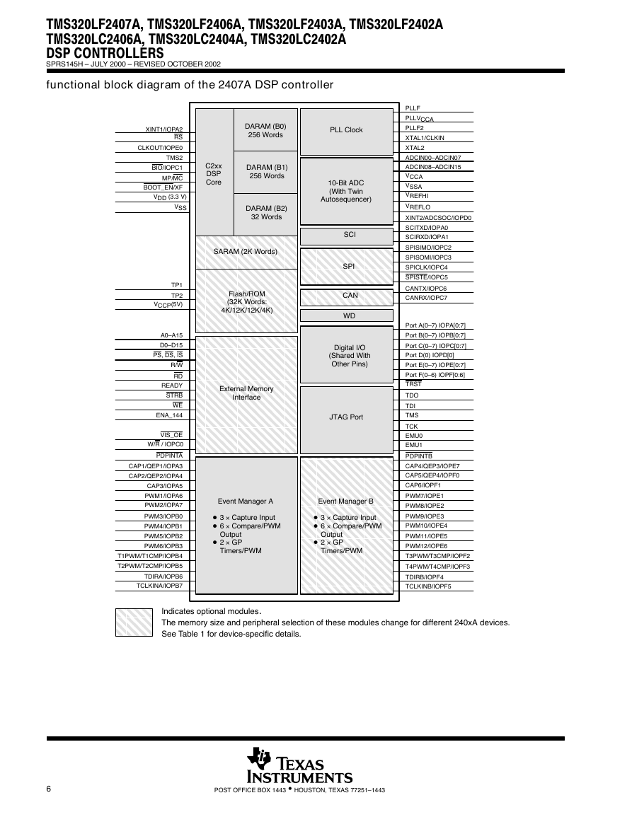
functional block diagram of the 2407A DSP controller
XINT1/IOPA2
RS
CLKOUT/IOPE0
TMS2
BIO/IOPC1
MP/MC
BOOT_EN/XF
VDD (3.3 V)
VSS
DARAM (B0)
256 Words
PLL Clock
C2xx
DSP
Core
DARAM (B1)
256 Words
DARAM (B2)
32 Words
10-Bit ADC
(With Twin
Autosequencer)
SCI
SPI
CAN
WD
JTAG Port
SARAM (2K Words)
External Memory
Interface
Digital I/O
(Shared With
Other Pins)
Flash/ROM
(32K Words:
4K/12K/12K/4K)
ÈÈÈÈÈÈÈ
ÈÈÈÈÈÈÈ
ÈÈÈÈÈÈÈ
ÈÈÈÈÈÈÈ
ÈÈÈÈÈÈÈ
ÈÈÈÈÈÈÈ
ÈÈÈÈÈÈÈ
ÈÈÈÈÈÈÈ
ÈÈÈÈÈÈÈ
ÈÈÈÈÈÈÈ
ÈÈÈÈÈÈÈ
ÈÈÈÈÈÈÈ
ÈÈÈÈÈÈÈ
ÈÈÈÈÈÈÈ
ÈÈÈÈÈÈÈ
ÈÈÈÈÈÈÈ
ÈÈÈÈÈÈÈ
ÈÈÈÈÈÈÈ
ÈÈÈÈÈÈÈ
ÈÈÈÈÈÈÈ
ÈÈÈÈÈÈÈ
ÈÈÈÈÈÈÈÈÈÈÈÈÈÈ
ÈÈÈÈÈÈÈ
ÈÈÈÈÈÈÈ
ÈÈÈÈÈÈÈ
ÈÈÈÈÈÈÈ
ÈÈÈÈÈÈÈ
ÈÈÈÈÈÈÈ
ÈÈÈÈÈÈÈ
ÈÈÈÈÈÈÈ
ÈÈÈÈÈÈÈ
D 3 × Capture Input
D 6 × Compare/PWM
D 3 × Capture Input
D 6 × Compare/PWM
Event Manager A
Event Manager B
Output
D 2 × GP
Timers/PWM
Output
D 2 × GP
Timers/PWM
TP1
TP2
VCCP(5V)
A0–A15
D0–D15
PS, DS, IS
R/W
RD
READY
STRB
WE
ENA_144
VIS_OE
W/R / IOPC0
PDPINTA
CAP1/QEP1/IOPA3
CAP2/QEP2/IOPA4
CAP3/IOPA5
PWM1/IOPA6
PWM2/IOPA7
PWM3/IOPB0
PWM4/IOPB1
PWM5/IOPB2
PWM6/IOPB3
T1PWM/T1CMP/IOPB4
T2PWM/T2CMP/IOPB5
TDIRA/IOPB6
TCLKINA/IOPB7
PLLF
PLLVCCA
PLLF2
XTAL1/CLKIN
XTAL2
ADCIN00–ADCIN07
ADCIN08–ADCIN15
VCCA
VSSA
VREFHI
VREFLO
XINT2/ADCSOC/IOPD0
SCITXD/IOPA0
SCIRXD/IOPA1
SPISIMO/IOPC2
SPISOMI/IOPC3
SPICLK/IOPC4
SPISTE/IOPC5
CANTX/IOPC6
CANRX/IOPC7
Port A(0–7) IOPA[0:7]
Port B(0–7) IOPB[0:7]
Port C(0–7) IOPC[0:7]
Port D(0) IOPD[0]
Port E(0–7) IOPE[0:7]
Port F(0–6) IOPF[0:6]
TRST
TDO
TDI
TMS
TCK
EMU0
EMU1
PDPINTB
CAP4/QEP3/IOPE7
CAP5/QEP4/IOPF0
CAP6/IOPF1
PWM7/IOPE1
PWM8/IOPE2
PWM9/IOPE3
PWM10/IOPE4
PWM11/IOPE5
PWM12/IOPE6
T3PWM/T3CMP/IOPF2
T4PWM/T4CMP/IOPF3
TDIRB/IOPF4
TCLKINB/IOPF5
ÈÈÈ
ÈÈÈ
ÈÈÈ
Indicates optional modules.
The memory size and peripheral selection of these modules change for different 240xA devices.
See Table 1 for device-specific details.
6
POST OFFICE BOX 1443 • HOUSTON, TEXAS 77251–1443
�
TMS320LF2407A, TMS320LF2406A, TMS320LF2403A, TMS320LF2402A
TMS320LC2406A, TMS320LC2404A, TMS320LC2402A
DSP CONTROLLERS
SPRS145H – JULY 2000 – REVISED OCTOBER 2002
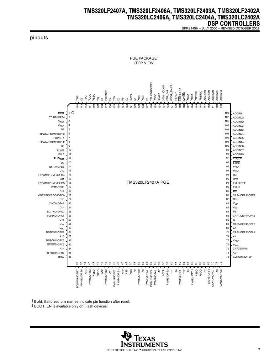
pinouts
PGE PACKAGE†
(TOP VIEW)
S
M
T
6
D
O
D
D
V
O
S
S
V
O
D
T
I
D
T
5
D
I
B
T
N
P
D
P
K
C
T
4
D
3
D
S
R
2
D
6
F
P
O
I
D
D
V
S
S
V
1
D
0
D
5
F
P
O
I
/
I
B
N
K
L
C
T
O
S
S
V
2
L
A
T
X
‡
/
F
X
N
E
_
T
O
O
B
4
4
1
_
A
N
E
1
C
P
O
I
/
O
B
I
Y
D
A
E
R
C
M
P
M
/
A
S
S
V
A
C
C
V
I
H
F
E
R
V
O
L
F
E
R
V
I
8
0
N
C
D
A
I
0
0
N
C
D
A
I
9
0
N
C
D
A
I
1
0
N
C
D
A
I
0
1
N
C
D
A
I
/
N
K
L
C
1
L
A
T
X
TRST
TDIRB/IOPF4
VSSO
VDDO
D7
T4PWM/T4CMP/IOPF3
PDPINTA
T3PWM/T3CMP/IOPF2
D8
PLLF2
PLLF
PLLVCCA
PLLVCCA
D9
TDIRA/IOPB6
D10
T1PWM/T1CMP/IOPB4
D11
T2PWM/T2CMP/IOPB5
W/R/IOPC0
D12
XINT2/ADCSOC/IOPD0
D13
XINT1/IOPA2
D14
SCITXD/IOPA0
SCIRXD/IOPA1
D15
VSS
VDD
SPISIMO/IOPC2
A15
SPISOMI/IOPC3
SPISTE/IOPC5
A14
SPICLK/IOPC4
TMS2
1
2
3
4
5
6
7
8
9
10
11
12
13
14
15
16
17
18
19
20
21
22
23
24
25
26
27
28
29
30
31
32
33
34
35
36
4
4
1
3
4
1
2
4
1
1
4
1
0
4
1
9
3
1
8
3
1
7
3
1
6
3
1
5
3
1
4
3
1
3
3
1
2
3
1
1
3
1
0
3
1
9
2
1
8
2
1
7
2
1
6
2
1
5
2
1
4
2
1
3
2
1
2
2
1
1
2
1
0
2
1
9
1
1
8
1
1
7
1
1
6
1
1
5
1
1
4
1
1
3
1
1
2
1
1
1
1
1
0
1
1
9
0
1
TMS320LF2407A PGE
108
107
106
105
104
103
102
101
100
99
98
97
96
95
94
93
92
91
90
89
88
87
86
85
84
83
82
81
80
79
78
77
76
75
74
73
ADCIN11
ADCIN02
ADCIN12
ADCIN03
ADCIN13
ADCIN04
ADCIN05
ADCIN14
ADCIN06
ADCIN07
ADCIN15
VIS_OE
STRB
VDDO
VSSO
RD
R/W
EMU1/OFF
EMU0
WE
CAP4/QEP3/IOPE7
DS
VDD
VSS
PS
CAP1/QEP1/IOPA3
IS
CAP5/QEP4/IOPF0
A0
CAP2/QEP2/IOPA4
A1
VDDO
VSSO
CAP3/IOPA5
A2
CLKOUT/IOPE0
7
3
8
3
9
3
0
4
1
4
2
4
3
4
4
4
5
4
6
4
7
4
8
4
9
4
0
5
1
5
2
5
3
5
4
5
5
5
6
5
7
5
8
5
9
5
0
6
1
6
2
6
3
6
4
6
5
6
6
6
7
6
8
6
9
6
0
7
1
7
2
7
3
1
A
3
B
P
O
I
/
6
M
W
P
6
E
P
O
I
/
2
1
M
W
P
7
B
P
O
I
/
I
A
N
K
L
C
T
O
S
S
V
O
D
D
V
2
1
A
1
1
A
2
B
P
O
I
/
5
M
W
P
1
B
P
O
I
/
4
M
W
P
5
E
P
O
I
/
1
1
M
W
P
0
1
A
S
S
V
D
D
V
9
A
8
A
0
B
P
O
I
/
3
M
W
P
7
A
P
O
I
/
2
M
W
P
4
E
P
O
I
/
0
1
M
W
P
6
A
P
O
I
/
1
M
W
P
7
A
P
C
C
V
3
E
P
O
I
/
9
M
W
P
6
A
1
P
T
2
E
P
O
I
/
8
M
W
P
5
A
2
P
T
1
E
P
O
I
/
7
M
W
P
4
A
O
S
S
V
O
D
D
V
1
F
P
O
I
/
6
P
A
C
7
C
P
O
I
/
X
R
N
A
C
3
A
6
C
P
O
I
/
X
T
N
A
C
† Bold, italicized pin names indicate pin function after reset.
‡ BOOT_EN is available only on Flash devices.
POST OFFICE BOX 1443 • HOUSTON, TEXAS 77251–1443
7
�
TMS320LF2407A, TMS320LF2406A, TMS320LF2403A, TMS320LF2402A
TMS320LC2406A, TMS320LC2404A, TMS320LC2402A
DSP CONTROLLERS
SPRS145H – JULY 2000 – REVISED OCTOBER 2002
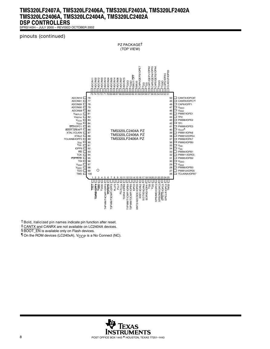
pinouts (continued)
PZ PACKAGE†
(TOP VIEW)
I
1
1
N
C
D
A
I
2
0
N
C
D
A
I
2
1
N
C
D
A
I
3
0
N
C
D
A
I
3
1
N
C
D
A
I
4
0
N
C
D
A
I
5
0
N
C
D
A
I
4
1
N
C
D
A
I
6
0
N
C
D
A
I
7
0
N
C
D
A
I
5
1
N
C
D
A
7
E
P
O
I
/
3
P
E
Q
4
P
A
C
/
0
U
M
E
3
A
P
O
0
F
P
O
4
A
P
O
I
/
I
/
I
/
1
P
E
Q
1
D
P
D
A
V C
S
S
V
/
4
P
E
Q
5
P
A
C
/
2
P
E
Q
2
P
A
C
/
0
E
P
O
I
/
T
U
O
K
L
C
5
A
P
O
I
/
O
3
D
P
D
A
V C
O
S
S
V
F
F
O
/
O
D
D
V
O
S
S
V
1
U
M
E
75
74
73
72
71
70
69
68
67
66
65
64
63
62
61
60
59
58
57
56
55
54
53
52
51
ADCIN10
ADCIN01
ADCIN09
ADCIN00
ADCIN08
VREFLO
VREFHI
VCCA
VSSA
BIO/IOPC1
BOOT_EN/XF§
XTAL1/CLKIN
XTAL2
TCLKINB/IOPF5
VSS
VDD
IOPF6
RS
TCK
PDPINTB
TDI
VSSO
VDDO
TDO
TMS
76
77
78
79
80
81
82
83
84
85
86
87
88
89
90
91
92
93
94
95
96
97
98
99
100
TMS320LC2404A PZ
TMS320LC2406A PZ
TMS320LF2406A PZ
50
49
48
47
46
45
44
43
42
41
40
39
38
37
36
35
34
33
32
31
30
29
28
27
26
CANTX/IOPC6‡
CANRX/IOPC7‡
CAP6/IOPF1
VDDO
VSSO
PWM7/IOPE1
TP2
PWM8/IOPE2
TP1
PWM9/IOPE3
¶
VCCP
PWM1/IOPA6
PWM10/IOPE4
PWM2/IOPA7
PWM3/IOPB0
VDD
VSS
PWM4/IOPB1
PWM11/IOPE5
PWM5/IOPB2
VDDO
VSSO
PWM6/IOPB3
PWM12/IOPE6
TCLKINA/IOPB7
987654321
10
11
12
13
14
15
16
17
18
19
20
21
22
23
24
25
F
L
L
P
A
C
C
V
L
L
P
6
B
P
O
I
/
A
R
D
T
I
2
F
L
L
P
T
S
R
T
4
4
F
F
P
P
O
O
O
O
S
S
S
S
V
V
O
D
D
V
I
I
/
/
B
B
R
R
D
D
T
T
I
I
3
F
P
O
I
/
/
P
M
C
4
T
M
W
P
4
T
I
A
T
N
P
D
P
2
F
P
O
I
/
/
P
M
C
3
T
M
W
P
3
T
1
A
P
O
S
S
V
D
D
V
I
/
D
X
R
C
S
I
2
C
P
O
I
/
I
O
M
S
P
S
I
3
C
P
O
I
/
I
M
O
S
P
S
I
5
C
P
O
I
/
E
T
S
P
S
I
4
C
P
O
2
S
M
T
I
/
K
L
C
P
S
I
2
A
P
O
I
/
1
T
N
X
I
0
A
P
O
I
/
D
X
T
C
S
I
4
B
P
O
I
5
B
P
O
I
0
C
P
O
I
/
/
P
M
C
1
T
M
W
P
1
T
/
/
P
M
C
2
T
M
W
P
2
T
0
D
P
O
I
/
C
O
S
C
D
A
2
T
N
X
I
/
† Bold, italicized pin names indicate pin function after reset.
‡ CANTX and CANRX are not available on LC2404A devices.
§ BOOT_EN is available only on Flash devices.
¶ On the ROM devices (LC240xA), VCCP is a No Connect (NC).
8
POST OFFICE BOX 1443 • HOUSTON, TEXAS 77251–1443
�


 2023年江西萍乡中考道德与法治真题及答案.doc
 2012年重庆南川中考生物真题及答案.doc
 2013年江西师范大学地理学综合及文艺理论基础考研真题.doc
 2020年四川甘孜小升初语文真题及答案I卷.doc
 2020年注册岩土工程师专业基础考试真题及答案.doc
 2023-2024学年福建省厦门市九年级上学期数学月考试题及答案.doc
 2021-2022学年辽宁省沈阳市大东区九年级上学期语文期末试题及答案.doc
 2022-2023学年北京东城区初三第一学期物理期末试卷及答案.doc
 2018上半年江西教师资格初中地理学科知识与教学能力真题及答案.doc
 2012年河北国家公务员申论考试真题及答案-省级.doc
 2020-2021学年江苏省扬州市江都区邵樊片九年级上学期数学第一次质量检测试题及答案.doc
 2022下半年黑龙江教师资格证中学综合素质真题及答案.doc