General Description
The MAX30205 temperature sensor accurately measures
temperature and provide an overtemperature alarm/
interrupt/shutdown output. This device converts the
temperature measurements to digital form using a high-
resolution, sigma-delta, analog-to-digital converter (ADC).
Accuracy meets clinical thermometry specification of
the ASTM E1112 when soldered on the final PCB.
Communication is through an I2C-compatible, 2-wire
serial interface.
The I2C serial interface accepts standard write byte, read
byte, send byte, and receive byte commands to read the
temperature data and configure the behavior of the open-
drain overtemperature shutdown output.
The MAX30205 features three address select lines with a
total of 32 available addresses. The sensor has a 2.7V to
3.3V supply voltage range, low 600µA supply current, and
a lockup-protected I2C-compatible interface that make it
ideal for wearable fitness and medical applications.
This device is available in an 8-pin TDFN package and
operates over the 0NC to +50NC temperature range.
Applications
● Fitness
● Medical
Typical Application Circuit
Benefits and Features
● High Accuracy and Low-Voltage Operation Aids
Designers in Meeting Error and Power Budgets
• 0.1°C Accuracy (37°C to 39°C)
• 16-Bit (0.00390625°C) Temperature Resolution
• 2.7V to 3.3V Supply Voltage Range
● One-Shot and Shutdown Modes Help Reduce Power
Usage
● 600μA (typ) Operating Supply Current
● Digital Functions Make Integration Easier into Any
System
• Selectable Timeout Prevents Bus Lockup
• Separate Open-Drain OS Output Operates as
Interrupt or Comparator/Thermostat Output
Ordering Information appears at end of data sheet.
4.7kΩ
TO I2C
MASTER
+2.7V TO +3.3V
MAX30205
SDA
SCL
OS
GND
VDD
A0
A1
A2
0.1µF
19-8505; Rev 0; 3/16
MAX30205Human Body Temperature Sensor�
Absolute Maximum Ratings
(All voltages relative to GND.)
Voltage Range on VDD, SDA, SCL, A0, A1 ............-0.3V to +4V
Voltage Range on A2, OS ........................ -0.3V to (VDD + 0.3V)
Input Current at Any Pin ....................................................+5mA
Package Input Current ....................................................+20mA
Continuous Power Dissipation (TA = +70°C)
TDFN (derate 24.4mW/NC above +70°C) ...............1951.2mW
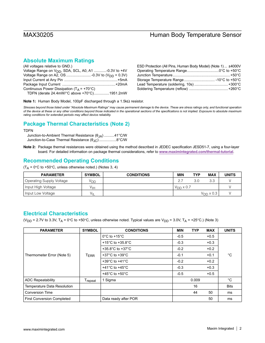
ESD Protection (All Pins, Human Body Model) (Note 1) ... ±4000V
Operating Temperature Range ...............................0NC to +50°C
Junction Temperature ........................................................+50°C
Storage Temperature Range .............................. -10NC to +50°C
Lead Temperature (soldering, 10s) .................................+300°C
Soldering Temperature (reflow) ......................................+260°C
Note 1: Human Body Model, 100pF discharged through a 1.5kI resistor.
Stresses beyond those listed under “Absolute Maximum Ratings” may cause permanent damage to the device. These are stress ratings only, and functional operation
of the device at these or any other conditions beyond those indicated in the operational sections of the specifications is not implied. Exposure to absolute maximum
rating conditions for extended periods may affect device reliability.
Package Thermal Characteristics (Note 2)
TDFN
Junction-to-Ambient Thermal Resistance (θJA) ..........41°C/W
Junction-to-Case Thermal Resistance (θJC) .................8°C/W
Note 2: Package thermal resistances were obtained using the method described in JEDEC specification JESD51-7, using a four-layer
board. For detailed information on package thermal considerations, refer to www.maximintegrated.com/thermal-tutorial.
Recommended Operating Conditions
(TA = 0°C to +50°C, unless otherwise noted.) (Notes 3, 4)
PARAMETER
SYMBOL
CONDITIONS
Operating Supply Voltage
Input High Voltage
Input Low Voltage
VDD
VIH
VIL
MIN
2.7
TYP
3.0
MAX
3.3
VDD x 0.7
VDD x 0.3
UNITS
V
V
V
Electrical Characteristics
(VDD = 2.7V to 3.3V, TA = 0°C to +50°C, unless otherwise noted. Typical values are VDD = 3.0V, TA = +25NC.) (Note 3)
PARAMETER
SYMBOL
CONDITIONS
Thermometer Error (Note 5)
TERR
ADC Repeatability
Temperature Data Resolution
Conversion Time
First Conversion Completed
Trepeat
0°C to +15°C
+15°C to +35.8°C
+35.8°C to +37°C
+37°C to +39°C
+39°C to +41°C
+41°C to +45°C
+45°C to +50°C
1 Sigma
Data ready after POR
MIN
-0.5
-0.3
-0.2
-0.1
-0.2
-0.3
-0.5
TYP
0.009
16
44
MAX
+0.5
+0.3
+0.2
+0.1
+0.2
+0.3
+0.5
50
50
UNITS
°C
°C
Bits
ms
ms
Maxim Integrated │ 2
www.maximintegrated.comMAX30205Human Body Temperature Sensor�
Electrical Characteristics (continued)
(VDD = 2.7V to 3.3V, TA = 0°C to +50°C, unless otherwise noted. Typical values are VDD = 3.0V, TA = +25NC.) (Note 3)
PARAMETER
SYMBOL
CONDITIONS
MIN
TYP
600
1.65
80
75
2.26
130
0.005
0.005
5
MAX
925
3.5
6
UNITS
µA
Conversions
°C
°C
V
mV
µA
µA
pF
µA
V
V
1
1
1
0.8
0.4
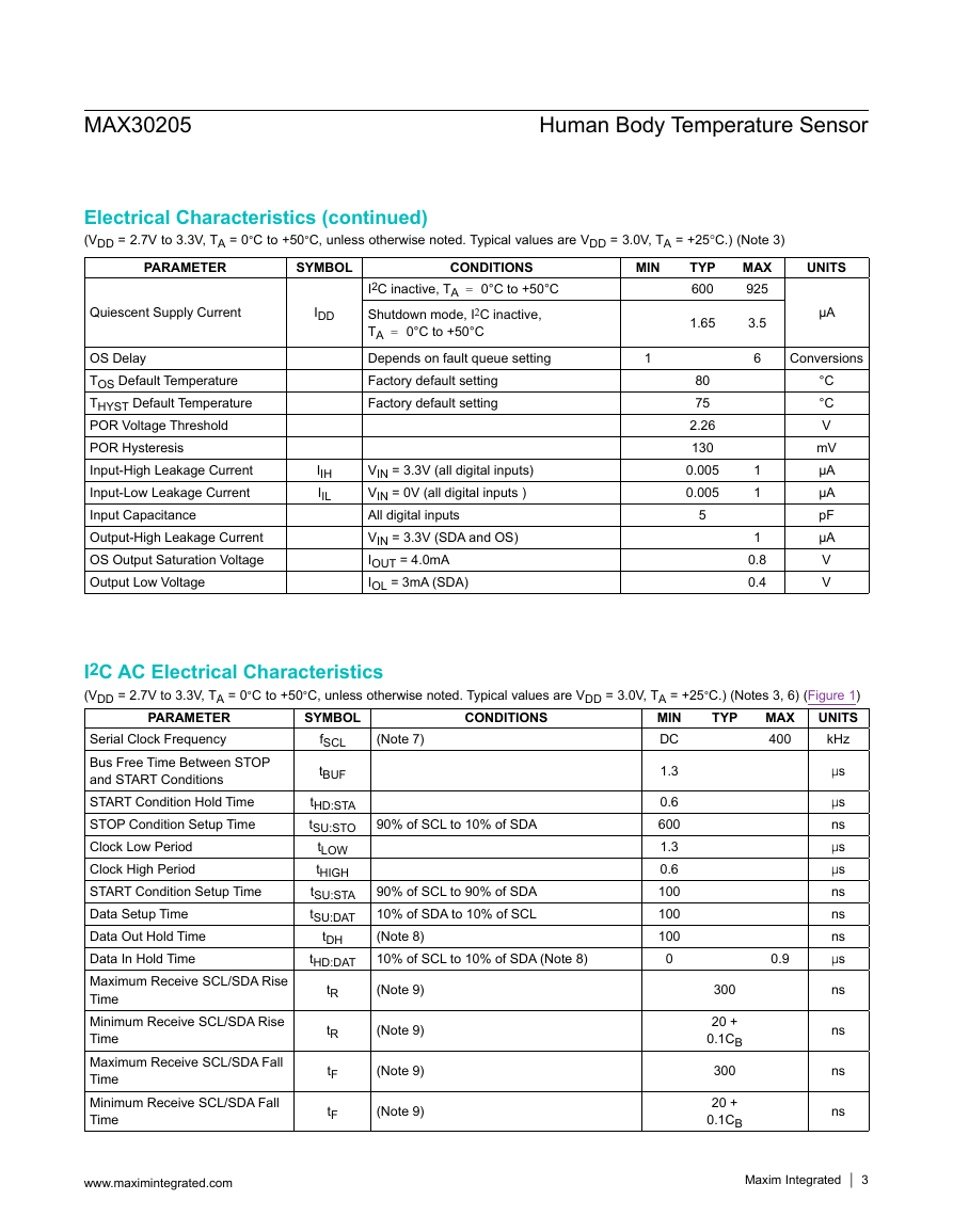
I2C inactive, TA = 0°C to +50°C
Shutdown mode, I2C inactive,
TA = 0°C to +50°C
Depends on fault queue setting
Factory default setting
Factory default setting
1
Quiescent Supply Current
IDD
OS Delay
TOS Default Temperature
THYST Default Temperature
POR Voltage Threshold
POR Hysteresis
Input-High Leakage Current
Input-Low Leakage Current
Input Capacitance
Output-High Leakage Current
OS Output Saturation Voltage
Output Low Voltage
IIH
IIL
VIN = 3.3V (all digital inputs)
VIN = 0V (all digital inputs )
All digital inputs
VIN = 3.3V (SDA and OS)
IOUT = 4.0mA
IOL = 3mA (SDA)
I2C AC Electrical Characteristics
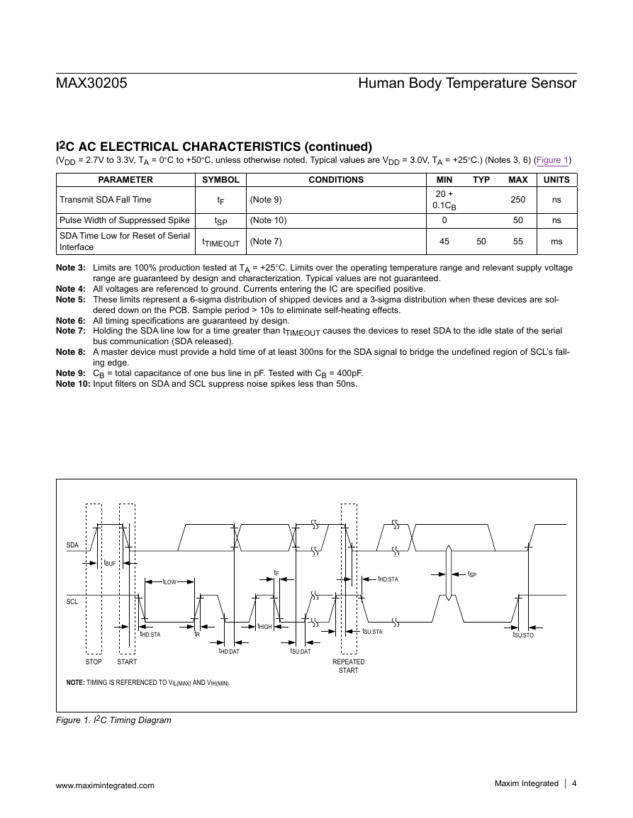
(VDD = 2.7V to 3.3V, TA = 0°C to +50°C, unless otherwise noted. Typical values are VDD = 3.0V, TA = +25°C.) (Notes 3, 6) (Figure 1)
UNITS
kHz
CONDITIONS
MAX
400
SYMBOL
TYP
MIN
DC
PARAMETER
Serial Clock Frequency
Bus Free Time Between STOP
and START Conditions
START Condition Hold Time
STOP Condition Setup Time
Clock Low Period
Clock High Period
START Condition Setup Time
Data Setup Time
Data Out Hold Time
Data In Hold Time
Maximum Receive SCL/SDA Rise
Time
Minimum Receive SCL/SDA Rise
Time
Maximum Receive SCL/SDA Fall
Time
Minimum Receive SCL/SDA Fall
Time
fSCL
(Note 7)
1.3
0.6
600
1.3
0.6
100
100
100
0
tBUF
tHD:STA
tSU:STO
tLOW
tHIGH
tSU:STA
tSU:DAT
tDH
tHD:DAT
tR
tR
tF
tF
90% of SCL to 10% of SDA
90% of SCL to 90% of SDA
10% of SDA to 10% of SCL
(Note 8)
10% of SCL to 10% of SDA (Note 8)
(Note 9)
(Note 9)
(Note 9)
(Note 9)
0.9
300
20 +
0.1CB
300
20 +
0.1CB
Fs
Fs
ns
Fs
Fs
ns
ns
ns
Fs
ns
ns
ns
ns
Maxim Integrated │ 3
www.maximintegrated.comMAX30205Human Body Temperature Sensor�
I2C AC ELECTRICAL CHARACTERISTICS (continued)
(VDD = 2.7V to 3.3V, TA = 0°C to +50°C, unless otherwise noted. Typical values are VDD = 3.0V, TA = +25°C.) (Notes 3, 6) (Figure 1)
UNITS
CONDITIONS
PARAMETER
TYP
MAX
SYMBOL
Transmit SDA Fall Time
Pulse Width of Suppressed Spike
SDA Time Low for Reset of Serial
Interface
tF
tSP
(Note 9)
(Note 10)
tTIMEOUT
(Note 7)
MIN
20 +
0.1CB
0
45
50
250
50
55
ns
ns
ms
Note 3: Limits are 100% production tested at TA = +25NC. Limits over the operating temperature range and relevant supply voltage
range are guaranteed by design and characterization. Typical values are not guaranteed.
Note 4: All voltages are referenced to ground. Currents entering the IC are specified positive.
Note 5: These limits represent a 6-sigma distribution of shipped devices and a 3-sigma distribution when these devices are sol-
dered down on the PCB. Sample period > 10s to eliminate self-heating effects.
Note 6: All timing specifications are guaranteed by design.
Note 7: Holding the SDA line low for a time greater than tTIMEOUT causes the devices to reset SDA to the idle state of the serial
Note 8: A master device must provide a hold time of at least 300ns for the SDA signal to bridge the undefined region of SCL’s fall-
bus communication (SDA released).
ing edge.
Note 9: CB = total capacitance of one bus line in pF. Tested with CB = 400pF.
Note 10: Input filters on SDA and SCL suppress noise spikes less than 50ns.
SDA
SCL
tBUF
tLOW
tHD:STA
tR
tF
tHIGH
STOP
START
NOTE: TIMING IS REFERENCED TO VIL(MAX) AND VIH(MIN).
tHD:DAT
tSU:DAT
Figure 1. I2C Timing Diagram
tHD:STA
tSP
tSU:STA
REPEATED
START
tSU:STO
Maxim Integrated │ 4
www.maximintegrated.comMAX30205Human Body Temperature Sensor�
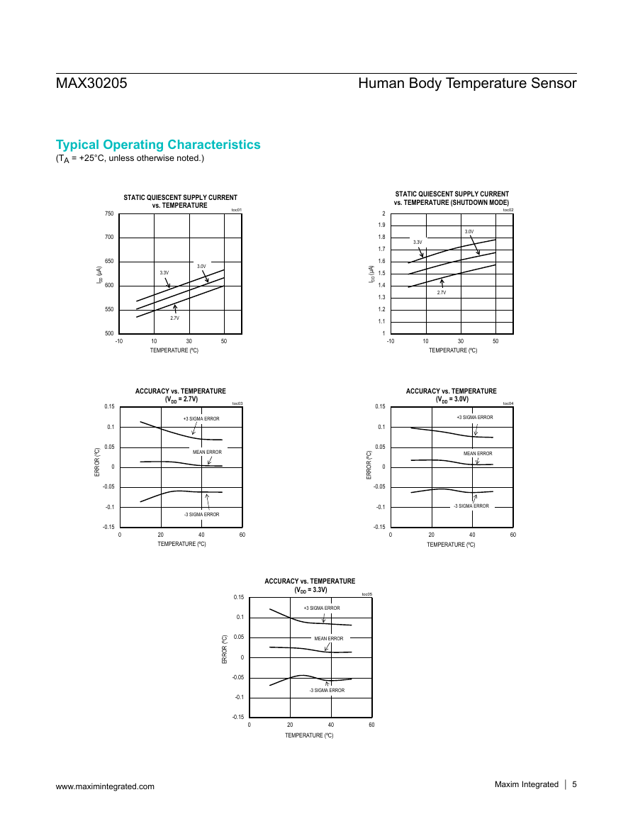
Typical Operating Characteristics
(TA = +25°C, unless otherwise noted.)
750
700
650
600
550
500
)
A
μ
(
D
D
I
)
C
º
(
R
O
R
R
E
0.15
0.1
0.05
0
-0.05
-0.1
-0.15
STATIC QUIESCENT SUPPLY CURRENT
vs. TEMPERATURE
toc01
3.3V
3.0V
2.7V
-10
10
TEMPERATURE (ºC)
30
50
ACCURACY vs. TEMPERATURE
(VDD = 2.7V)
toc03
+3 SIGMA ERROR
MEAN ERROR
-3 SIGMA ERROR
0
20
40
TEMPERATURE (ºC)
60
)
A
μ
(
D
D
I
2
1.9
1.8
1.7
1.6
1.5
1.4
1.3
1.2
1.1
1
)
C
º
(
R
O
R
R
E
0.15
0.1
0.05
0
-0.05
-0.1
-0.15
STATIC QUIESCENT SUPPLY CURRENT
vs. TEMPERATURE (SHUTDOWN MODE)
toc02
3.0V
3.3V
2.7V
-10
10
30
50
TEMPERATURE (ºC)
ACCURACY vs. TEMPERATURE
(VDD = 3.0V)
toc04
+3 SIGMA ERROR
MEAN ERROR
-3 SIGMA ERROR
0
20
40
TEMPERATURE (ºC)
60
)
C
º
(
R
O
R
R
E
0.15
0.1
0.05
0
-0.05
-0.1
-0.15
ACCURACY vs. TEMPERATURE
(VDD = 3.3V)
toc05
+3 SIGMA ERROR
MEAN ERROR
-3 SIGMA ERROR
0
20
40
TEMPERATURE (ºC)
60
Maxim Integrated │ 5
www.maximintegrated.comMAX30205Human Body Temperature Sensor�
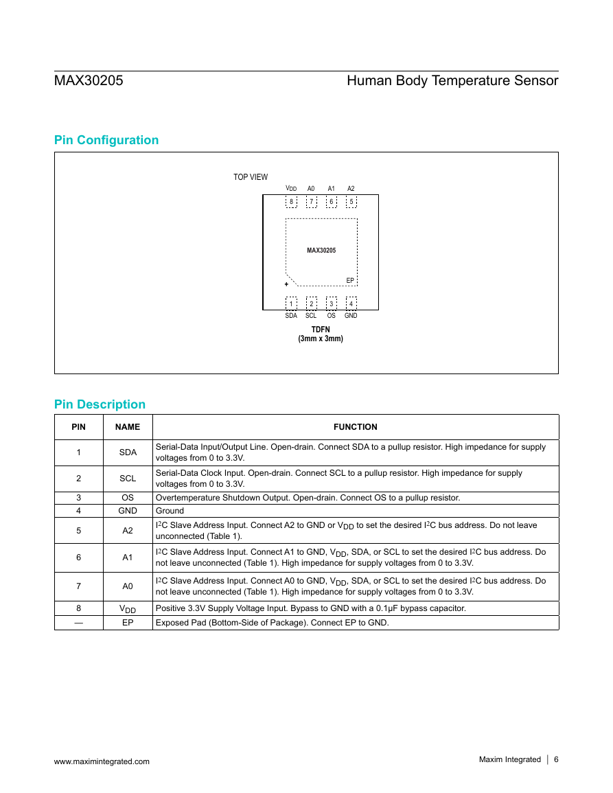
Pin Configuration
TOP VIEW
VDD
8
A0
7
A1
6
A2
5
MAX30205
EP
4
GND
+
1
SDA
3
2
OS
SCL
TDFN
(3mm x 3mm)
Pin Description
NAME
PIN
FUNCTION
1
2
3
4
5
6
7
8
—
SDA
SCL
OS
GND
A2
A1
A0
VDD
EP
Serial-Data Input/Output Line. Open-drain. Connect SDA to a pullup resistor. High impedance for supply
voltages from 0 to 3.3V.
Serial-Data Clock Input. Open-drain. Connect SCL to a pullup resistor. High impedance for supply
voltages from 0 to 3.3V.
Overtemperature Shutdown Output. Open-drain. Connect OS to a pullup resistor.
Ground
I2C Slave Address Input. Connect A2 to GND or VDD to set the desired I2C bus address. Do not leave
unconnected (Table 1).
I2C Slave Address Input. Connect A1 to GND, VDD, SDA, or SCL to set the desired I2C bus address. Do
not leave unconnected (Table 1). High impedance for supply voltages from 0 to 3.3V.
I2C Slave Address Input. Connect A0 to GND, VDD, SDA, or SCL to set the desired I2C bus address. Do
not leave unconnected (Table 1). High impedance for supply voltages from 0 to 3.3V.
Positive 3.3V Supply Voltage Input. Bypass to GND with a 0.1µF bypass capacitor.
Exposed Pad (Bottom-Side of Package). Connect EP to GND.
Maxim Integrated │ 6
www.maximintegrated.comMAX30205Human Body Temperature Sensor�
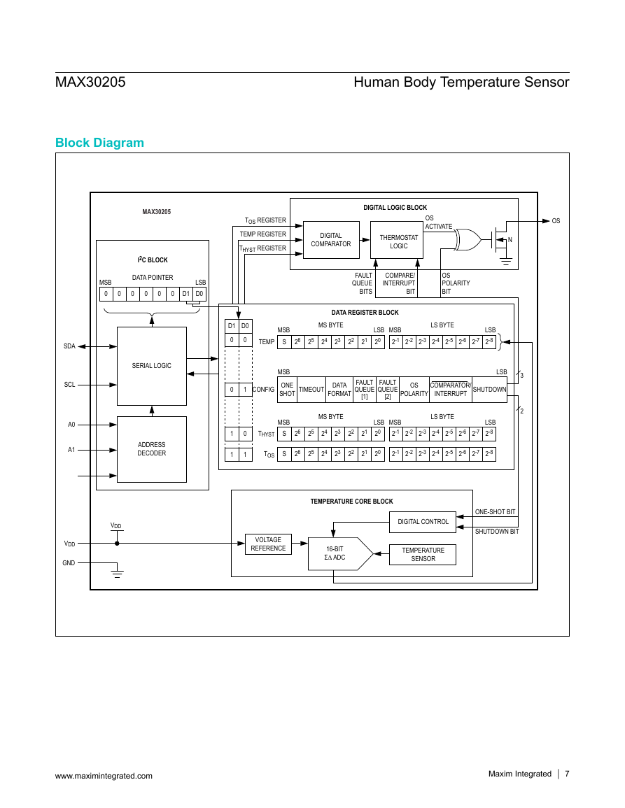
Block Diagram
MAX30205
I2C BLOCK
DIGITAL LOGIC BLOCK
TOS REGISTER
TEMP REGISTER
THYST REGISTER
DIGITAL
COMPARATOR
THERMOSTAT
LOGIC
OS
ACTIVATE
OS
N
MSB
0
0
0
0
0
DATA POINTER
LSB
0 D1 D0
SERIAL LOGIC
ADDRESS
DECODER
VDD
SDA
SCL
A0
A1
VDD
GND
FAULT
QUEUE
BITS
COMPARE/
INTERRUPT
BIT
OS
POLARITY
BIT
DATA REGISTER BLOCK
D1 D0
0
0
MSB
S
TEMP
MS BYTE
26
25
24
23
22
21
LSB
20
LS BYTE
MSB
LSB
2-1 2-2 2-3 2-4 2-5 2-6 2-7 2-8
0
1
CONFIG
MSB
ONE
SHOT TIMEOUT
DATA
FORMAT
FAULT
QUEUE
[1]
FAULT
QUEUE
[2]
OS
POLARITY
COMPARATOR/
INTERRUPT
SHUTDOWN
LSB
MSB
S
THYST
TOS
S
1
1
0
1
MS BYTE
26
26
25
25
24
24
23
23
22
22
21
21
LSB
20
LS BYTE
MSB
LSB
2-1 2-2 2-3 2-4 2-5 2-6 2-7 2-8
20
2-1 2-2 2-3 2-4 2-5 2-6 2-7 2-8
3
2
TEMPERATURE CORE BLOCK
VOLTAGE
REFERENCE
16-BIT
Σ∆ ADC
ONE-SHOT BIT
SHUTDOWN BIT
DIGITAL CONTROL
TEMPERATURE
SENSOR
Maxim Integrated │ 7
www.maximintegrated.comMAX30205Human Body Temperature Sensor�
Detailed Description
The MAX30205
temperature sensor measures
temperature and converts the data into digital form. An
I2C-compatible two-wire serial interface allows access
to conversion results. The device accepts standard I2C
commands to read the data, set the overtemperature alarm
(OS) trip thresholds, and configure other characteristics.
While reading the temperature register, any changes in
temperature are ignored until the read is completed. The
temperature register is updated for the new temperature
measurement upon completion of the read operation.
OS Output, TOS and THYST Limits
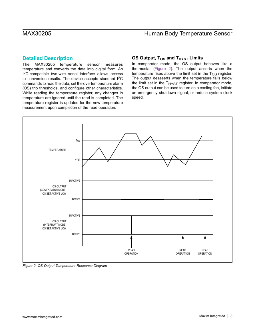
In comparator mode, the OS output behaves like a
thermostat (Figure 2). The output asserts when the
temperature rises above the limit set in the TOS register.
The output deasserts when the temperature falls below
the limit set in the THYST register. In comparator mode,
the OS output can be used to turn on a cooling fan, initiate
an emergency shutdown signal, or reduce system clock
speed.
TEMPERATURE
OS OUTPUT
(COMPARATOR MODE)
OS SET ACTIVE LOW
OS OUTPUT
(INTERRUPT MODE)
OS SET ACTIVE LOW
TOS
THYST
INACTIVE
ACTIVE
INACTIVE
ACTIVE
Figure 2. OS Output Temperature Response Diagram
READ
OPERATION
READ
OPERATION
READ
OPERATION
Maxim Integrated │ 8
www.maximintegrated.comMAX30205Human Body Temperature Sensor�



 2023年江西萍乡中考道德与法治真题及答案.doc
 2012年重庆南川中考生物真题及答案.doc
 2013年江西师范大学地理学综合及文艺理论基础考研真题.doc
 2020年四川甘孜小升初语文真题及答案I卷.doc
 2020年注册岩土工程师专业基础考试真题及答案.doc
 2023-2024学年福建省厦门市九年级上学期数学月考试题及答案.doc
 2021-2022学年辽宁省沈阳市大东区九年级上学期语文期末试题及答案.doc
 2022-2023学年北京东城区初三第一学期物理期末试卷及答案.doc
 2018上半年江西教师资格初中地理学科知识与教学能力真题及答案.doc
 2012年河北国家公务员申论考试真题及答案-省级.doc
 2020-2021学年江苏省扬州市江都区邵樊片九年级上学期数学第一次质量检测试题及答案.doc
 2022下半年黑龙江教师资格证中学综合素质真题及答案.doc