ARM Cortex-A53 MPCore Processor Technical Reference Manual
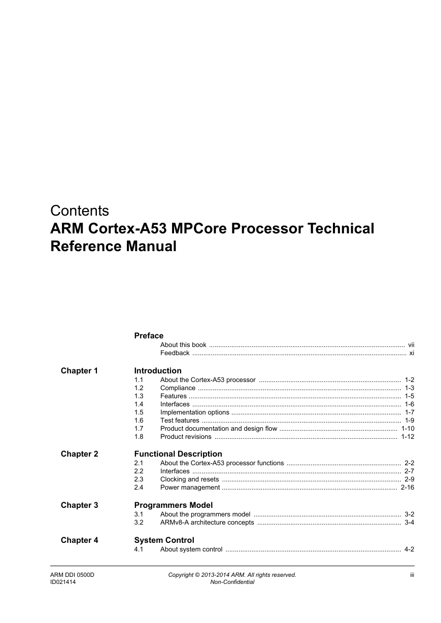
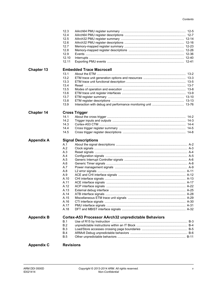
Contents
Preface
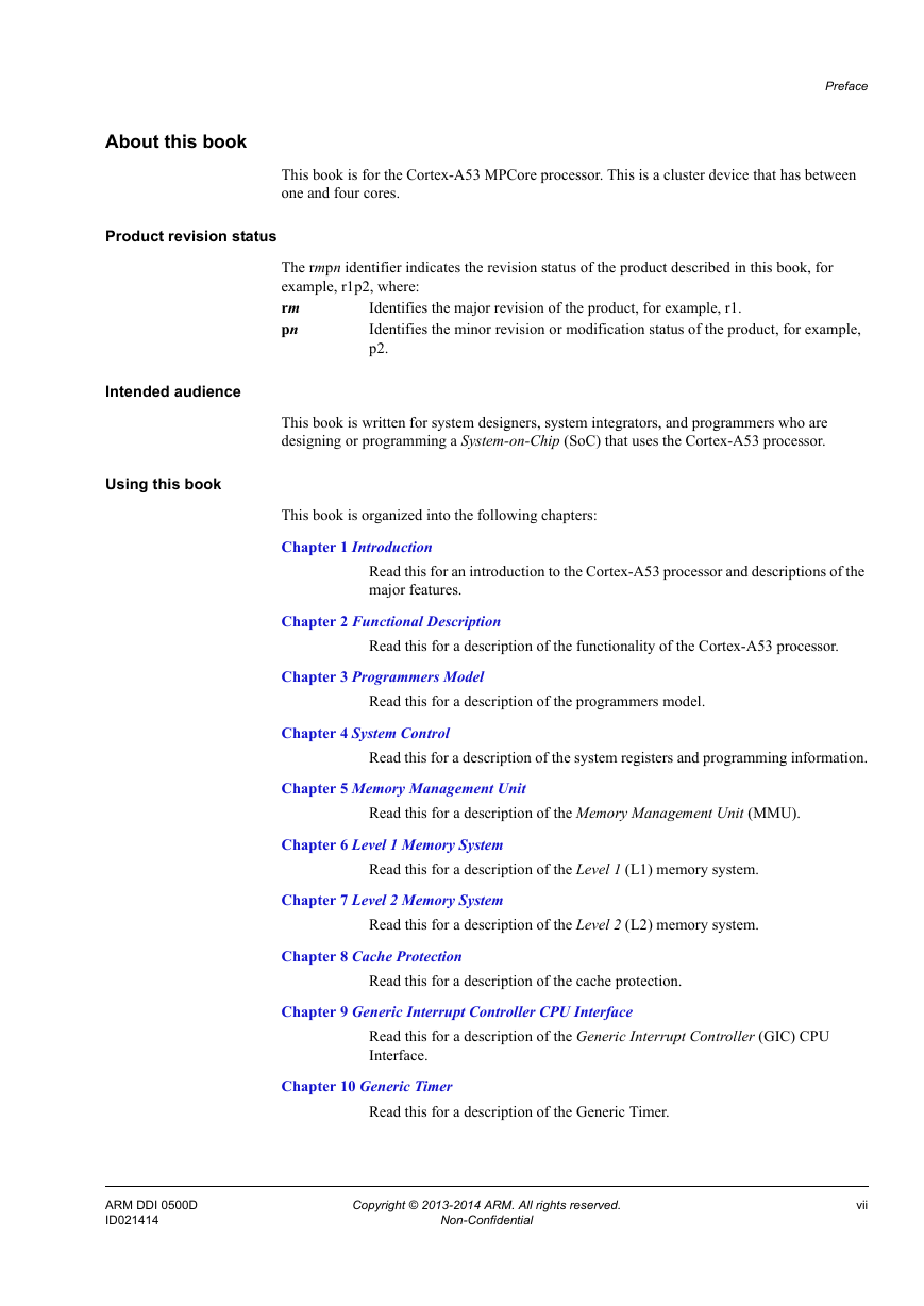
About this book
Product revision status
Intended audience
Using this book
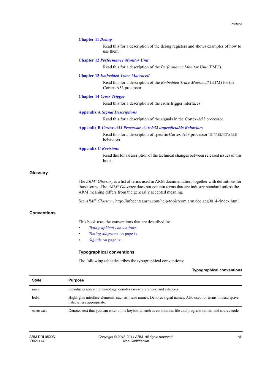
Glossary
Conventions
Additional reading
Feedback
Feedback on this product
Feedback on content
1: Introduction
1.1 About the Cortex-A53 processor
1.2 Compliance
1.2.1 ARM architecture
1.2.2 Interconnect architecture
1.2.3 Generic Interrupt Controller architecture
1.2.4 Generic Timer architecture
1.2.5 Debug architecture
1.2.6 Embedded Trace Macrocell architecture
1.3 Features
1.4 Interfaces
1.5 Implementation options
1.5.1 Processor configuration
1.6 Test features
1.7 Product documentation and design flow
1.7.1 Documentation
1.7.2 Design flow
1.8 Product revisions
2: Functional Description
2.1 About the Cortex-A53 processor functions
2.1.1 Instruction Fetch Unit
2.1.2 Data Processing Unit
2.1.3 Advanced SIMD and Floating-point Extension
2.1.4 Cryptography Extension
2.1.5 Translation Lookaside Buffer
2.1.6 Data side memory system
2.1.7 L2 memory system
2.1.8 Cache protection
2.1.9 Debug and trace
2.2 Interfaces
2.2.1 Master memory interface
2.2.2 Accelerator Coherency Port
2.2.3 External debug interface
2.2.4 Trace interface
2.2.5 CTI
2.2.6 DFT
2.2.7 MBIST
2.2.8 Q-channel
2.3 Clocking and resets
2.3.1 Clocks
2.3.2 Input synchronization
2.3.3 Resets
2.4 Power management
2.4.1 Power domains
2.4.2 Power modes
2.4.3 Event communication using WFE or SEV
2.4.4 Communication to the Power Management Controller
3: Programmers Model
3.1 About the programmers model
3.1.1 Advanced SIMD and Floating-point support
3.1.2 Memory model
3.1.3 Jazelle implementation
3.1.4 Modes of operation
3.2 ARMv8-A architecture concepts
3.2.1 Execution state
3.2.2 Exception levels
3.2.3 Security state
3.2.4 Rules for changing execution state
3.2.5 Stack pointer selection
3.2.6 ARMv8 security model
3.2.7 Instruction set state
3.2.8 AArch32 execution modes
4: System Control
4.1 About system control
4.1.1 AArch32 registers affected by CP15SDISABLE
4.2 AArch64 register summary
4.2.1 AArch64 identification registers
4.2.2 AArch64 exception handling registers
4.2.3 AArch64 virtual memory control registers
4.2.4 AArch64 other system control registers
4.2.5 AArch64 performance monitor registers
4.2.6 AArch64 reset registers
4.2.7 AArch64 secure registers
4.2.8 AArch64 virtualization registers
4.2.9 AArch64 GIC system registers
4.2.10 AArch64 Generic Timer registers
4.2.11 AArch64 thread registers
4.2.12 AArch64 implementation defined registers
4.2.13 AArch64 address registers
4.3 AArch64 register descriptions
4.3.1 Main ID Register, EL1
4.3.2 Multiprocessor Affinity Register
4.3.3 Revision ID Register
4.3.4 AArch32 Processor Feature Register 0
4.3.5 AArch32 Processor Feature Register 1
4.3.6 AArch32 Debug Feature Register 0
4.3.7 AArch32 Auxiliary Feature Register 0
4.3.8 AArch32 Memory Model Feature Register 0
4.3.9 AArch32 Memory Model Feature Register 1
4.3.10 AArch32 Memory Model Feature Register 2
4.3.11 AArch32 Memory Model Feature Register 3
4.3.12 AArch32 Instruction Set Attribute Register 0
4.3.13 AArch32 Instruction Set Attribute Register 1
4.3.14 AArch32 Instruction Set Attribute Register 2
4.3.15 AArch32 Instruction Set Attribute Register 3
4.3.16 AArch32 Instruction Set Attribute Register 4
4.3.17 AArch32 Instruction Set Attribute Register 5
4.3.18 AArch64 Processor Feature Register 0
4.3.19 AArch64 Debug Feature Register 0, EL1
4.3.20 AArch64 Instruction Set Attribute Register 0, EL1
4.3.21 AArch64 Memory Model Feature Register 0, EL1
4.3.22 Cache Size ID Register
4.3.23 Cache Level ID Register
4.3.24 Auxiliary ID Register
4.3.25 Cache Size Selection Register
4.3.26 Cache Type Register
4.3.27 Data Cache Zero ID Register
4.3.28 Virtualization Processor ID Register
4.3.29 Virtualization Multiprocessor ID Register
4.3.30 System Control Register, EL1
4.3.31 Auxiliary Control Register, EL1
4.3.32 Auxiliary Control Register, EL2
4.3.33 Auxiliary Control Register, EL3
4.3.34 Architectural Feature Access Control Register
4.3.35 System Control Register, EL2
4.3.36 Hypervisor Configuration Register
4.3.37 Hyp Debug Control Register
4.3.38 Architectural Feature Trap Register, EL2
4.3.39 Hyp System Trap Register
4.3.40 Hyp Auxiliary Configuration Register
4.3.41 System Control Register, EL3
4.3.42 Secure Configuration Register
4.3.43 Secure Debug Enable Register
4.3.44 Translation Table Base Register 0, EL1
4.3.45 Translation Table Base Register 1
4.3.46 Architectural Feature Trap Register, EL3
4.3.47 Monitor Debug Configuration Register, EL3
4.3.48 Translation Control Register, EL1
4.3.49 Translation Control Register, EL2
4.3.50 Virtualization Translation Control Register, EL2
4.3.51 Domain Access Control Register
4.3.52 Translation Table Base Register 0, EL3
4.3.53 Translation Control Register, EL3
4.3.54 Auxiliary Memory Attribute Indirection Register, EL1, EL2 and EL3
4.3.55 Auxiliary Fault Status Register 0, EL1, EL2 and EL3
4.3.56 Auxiliary Fault Status Register 1, EL1, EL2 and EL3
4.3.57 Exception Syndrome Register, EL1
4.3.58 Instruction Fault Status Register, EL2
4.3.59 Exception Syndrome Register, EL2
4.3.60 Exception Syndrome Register, EL3
4.3.61 Fault Address Register, EL1
4.3.62 Fault Address Register, EL2
4.3.63 Hypervisor IPA Fault Address Register, EL2
4.3.64 L2 Control Register
4.3.65 L2 Extended Control Register
4.3.66 L2 Auxiliary Control Register
4.3.67 Fault Address Register, EL3
4.3.68 Physical Address Register, EL1
4.3.69 Memory Attribute Indirection Register, EL1
4.3.70 Memory Attribute Indirection Register, EL2
4.3.71 Memory Attribute Indirection Register, EL3
4.3.72 Vector Base Address Register, EL1
4.3.73 Vector Base Address Register, EL2
4.3.74 Vector Base Address Register, EL3
4.3.75 Reset Vector Base Address Register, EL3
4.3.76 Reset Management Register
4.3.77 Interrupt Status Register
4.3.78 CPU Auxiliary Control Register, EL1
4.3.79 CPU Extended Control Register, EL1
4.3.80 CPU Memory Error Syndrome Register
4.3.81 L2 Memory Error Syndrome Register
4.3.82 Configuration Base Address Register, EL1
4.4 AArch32 register summary
4.4.1 c0 registers
4.4.2 c1 registers
4.4.3 c2 registers
4.4.4 c3 registers
4.4.5 c4 registers
4.4.6 c5 registers
4.4.7 c6 registers
4.4.8 c7 registers
4.4.9 c9 registers
4.4.10 c10 registers
4.4.11 c11 registers
4.4.12 c12 registers
4.4.13 c13 registers
4.4.14 c14 registers
4.4.15 c15 registers
4.4.16 64-bit registers
4.4.17 AArch32 Identification registers
4.4.18 AArch32 Virtual memory control registers
4.4.19 AArch32 Fault handling registers
4.4.20 AArch32 Other System control registers
4.4.21 AArch32 Address registers
4.4.22 AArch32 Thread registers
4.4.23 AArch32 Performance monitor registers
4.4.24 AArch32 Secure registers
4.4.25 AArch32 Virtualization registers
4.4.26 AArch32 GIC system registers
4.4.27 AArch32 Generic Timer registers
4.4.28 AArch32 Implementation defined registers
4.5 AArch32 register descriptions
4.5.1 Main ID Register
4.5.2 Multiprocessor Affinity Register
4.5.3 Revision ID Register
4.5.4 TCM Type Register
4.5.5 TLB Type Register
4.5.6 Processor Feature Register 0
4.5.7 Processor Feature Register 1
4.5.8 Debug Feature Register 0
4.5.9 Auxiliary Feature Register 0
4.5.10 Memory Model Feature Register 0
4.5.11 Memory Model Feature Register 1
4.5.12 Memory Model Feature Register 2
4.5.13 Memory Model Feature Register 3
4.5.14 Instruction Set Attribute Register 0
4.5.15 Instruction Set Attribute Register 1
4.5.16 Instruction Set Attribute Register 2
4.5.17 Instruction Set Attribute Register 3
4.5.18 Instruction Set Attribute Register 4
4.5.19 Instruction Set Attribute Register 5
4.5.20 Cache Size ID Register
4.5.21 Cache Level ID Register
4.5.22 Auxiliary ID Register
4.5.23 Cache Size Selection Register
4.5.24 Cache Type Register
4.5.25 Virtualization Processor ID Register
4.5.26 Virtualization Multiprocessor ID Register
4.5.27 System Control Register
4.5.28 Auxiliary Control Register
4.5.29 Architectural Feature Access Control Register
4.5.30 Secure Configuration Register
4.5.31 Secure Debug Enable Register
4.5.32 Non-Secure Access Control Register
4.5.33 Secure Debug Control Register
4.5.34 Hyp Auxiliary Control Register
4.5.35 Hyp System Control Register
4.5.36 Hyp Configuration Register
4.5.37 Hyp Configuration Register 2
4.5.38 Hyp Debug Control Register
4.5.39 Hyp Architectural Feature Trap Register
4.5.40 Translation Table Base Register 0
4.5.41 Translation Table Base Register 1
4.5.42 Translation Table Base Control Register
4.5.43 Hyp Translation Control Register
4.5.44 Virtualization Translation Control Register
4.5.45 Domain Access Control Register
4.5.46 Hyp System Trap Register
4.5.47 Hyp Auxiliary Configuration Register
4.5.48 Data Fault Status Register
4.5.49 Instruction Fault Status Register
4.5.50 Auxiliary Data Fault Status Register
4.5.51 Auxiliary Instruction Fault Status Register
4.5.52 Hyp Auxiliary Data Fault Status Syndrome Register
4.5.53 Hyp Auxiliary Instruction Fault Status Syndrome Register
4.5.54 Hyp Syndrome Register
4.5.55 Data Fault Address Register
4.5.56 Instruction Fault Address Register
4.5.57 Hyp Data Fault Address Register
4.5.58 Hyp Instruction Fault Address Register
4.5.59 Hyp IPA Fault Address Register
4.5.60 Physical Address Register
4.5.61 L2 Control Register
4.5.62 L2 Extended Control Register
4.5.63 Primary Region Remap Register
4.5.64 Memory Attribute Indirection Registers 0 and 1
4.5.65 Normal Memory Remap Register
4.5.66 Auxiliary Memory Attribute Indirection Register 0
4.5.67 Auxiliary Memory Attribute Indirection Register 1
4.5.68 Hyp Auxiliary Memory Attribute Indirection Register 0
4.5.69 Hyp Auxiliary Memory Attribute Indirection Register 1
4.5.70 Vector Base Address Register
4.5.71 Reset Management Register
4.5.72 Interrupt Status Register
4.5.73 Hyp Vector Base Address Register
4.5.74 FCSE Process ID Register
4.5.75 L2 Auxiliary Control Register
4.5.76 CPU Auxiliary Control Register
4.5.77 CPU Extended Control Register
4.5.78 CPU Memory Error Syndrome Register
4.5.79 L2 Memory Error Syndrome Register
4.5.80 Configuration Base Address Register
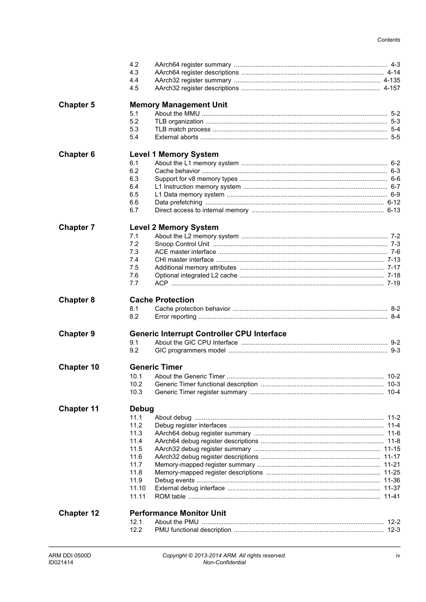
5: Memory Management Unit
5.1 About the MMU
5.2 TLB organization
5.2.1 Micro TLB
5.2.2 Main TLB
5.2.3 IPA cache RAM
5.2.4 Walk cache RAM
5.3 TLB match process
5.4 External aborts
5.4.1 External aborts on data read or write
6: Level 1 Memory System
6.1 About the L1 memory system
6.2 Cache behavior
6.2.1 Instruction cache disabled behavior
6.2.2 Instruction cache speculative memory accesses
6.2.3 Data cache disabled behavior
6.2.4 Data cache maintenance considerations
6.2.5 Data cache coherency
6.3 Support for v8 memory types
6.4 L1 Instruction memory system
6.4.1 Enabling program flow prediction
6.4.2 Program flow prediction
6.5 L1 Data memory system
6.5.1 Internal exclusive monitor
6.5.2 ACE transactions
6.5.3 CHI transactions
6.6 Data prefetching
6.6.1 Preload instructions
6.6.2 Data prefetching and monitoring
6.6.3 Non-temporal loads
6.6.4 Data Cache Zero
6.7 Direct access to internal memory
6.7.1 Data cache tag and data encoding
6.7.2 Instruction cache tag and data encoding
6.7.3 TLB RAM accesses
7: Level 2 Memory System
7.1 About the L2 memory system
7.2 Snoop Control Unit
7.2.1 Bus interface configuration signals
7.2.2 Snoop and maintenance requests
7.3 ACE master interface
7.3.1 Memory interface attributes
7.3.2 ACE transfers
7.3.3 Snoop channel properties
7.3.4 Read response
7.3.5 Write response
7.3.6 Barriers
7.3.7 AXI3 compatibility mode
7.3.8 AXI privilege information
7.4 CHI master interface
7.4.1 Memory interface attributes
7.4.2 CHI transfers
7.4.3 CHI channel properties
7.4.4 CHI transaction IDs
7.4.5 CHI nodes
7.5 Additional memory attributes
7.6 Optional integrated L2 cache
7.6.1 External aborts handling
7.7 ACP
7.7.1 Transfer size support
7.7.2 ACP user signals
7.7.3 ACP performance
8: Cache Protection
8.1 Cache protection behavior
8.2 Error reporting
9: Generic Interrupt Controller CPU Interface
9.1 About the GIC CPU Interface
9.1.1 Bypassing the CPU Interface
9.2 GIC programmers model
9.2.1 Memory map
9.2.2 CPU interface register summary
9.2.3 CPU interface register descriptions
9.2.4 Virtual interface control register summary
9.2.5 Virtual interface control register descriptions
9.2.6 Virtual CPU interface register summary
9.2.7 Virtual CPU interface register descriptions
10: Generic Timer
10.1 About the Generic Timer
10.2 Generic Timer functional description
10.3 Generic Timer register summary
10.3.1 AArch64 Generic Timer register summary
10.3.2 AArch32 Generic Timer register summary
11: Debug
11.1 About debug
11.1.1 Debug host
11.1.2 Protocol converter
11.1.3 Debug target
11.1.4 The debug unit
11.1.5 Self-hosted debug
11.2 Debug register interfaces
11.2.1 Processor interfaces
11.2.2 Effects of resets on debug registers
11.2.3 External access permissions
11.3 AArch64 debug register summary
11.4 AArch64 debug register descriptions
11.4.1 Debug Breakpoint Control Registers, EL1
11.4.2 Debug Watchpoint Control Registers, EL1
11.4.3 Debug Claim Tag Set register
11.5 AArch32 debug register summary
11.6 AArch32 debug register descriptions
11.6.1 Debug ID Register
11.6.2 Debug Device ID Register
11.6.3 Debug Device ID Register 1
11.7 Memory-mapped register summary
11.8 Memory-mapped register descriptions
11.8.1 External Debug Integration Mode Control Register
11.8.2 External Debug Device ID Register 0
11.8.3 External Debug Device ID Register 1
11.8.4 Peripheral Identification Registers
11.8.5 Component Identification Registers
11.9 Debug events
11.9.1 Watchpoint debug events
11.9.2 Debug OS Lock
11.10 External debug interface
11.10.1 Debug memory map
11.10.2 DBGPWRDUP debug signal
11.10.3 DBGL1RSTDISABLE debug signal
11.10.4 Changing the authentication signals
11.11 ROM table
11.11.1 ROM table register interface
11.11.2 ROM table register summary
11.11.3 ROM table register descriptions
11.11.4 Peripheral Identification Registers
11.11.5 Component Identification Registers
12: Performance Monitor Unit
12.1 About the PMU
12.2 PMU functional description
12.2.1 Event interface
12.2.2 System register and APB interface
12.2.3 Counters
12.2.4 PMU register interfaces
12.2.5 External register access permissions
12.3 AArch64 PMU register summary
12.4 AArch64 PMU register descriptions
12.4.1 Performance Monitors Control Register
12.4.2 Performance Monitors Common Event Identification Register 0
12.4.3 Performance Monitors Common Event Identification Register 1
12.5 AArch32 PMU register summary
12.6 AArch32 PMU register descriptions
12.6.1 Performance Monitors Control Register
12.6.2 Performance Monitors Common Event Identification Register 0
12.6.3 Performance Monitors Common Event Identification Register 1
12.7 Memory-mapped register summary
12.8 Memory-mapped register descriptions
12.8.1 Performance Monitor Configuration Register
12.8.2 Peripheral Identification Registers
12.8.3 Component Identification Registers
12.9 Events
12.10 Interrupts
12.11 Exporting PMU events
12.11.1 External hardware
12.11.2 Debug trace hardware
13: Embedded Trace Macrocell
13.1 About the ETM
13.2 ETM trace unit generation options and resources
13.3 ETM trace unit functional description
13.3.1 Processor interface
13.3.2 Trace generation
13.3.3 Filtering and triggering resources
13.3.4 FIFO
13.3.5 Trace out
13.3.6 Syncbridge
13.4 Reset
13.5 Modes of operation and execution
13.5.1 Controlling ETM trace unit programming
13.5.2 Programming and reading ETM trace unit registers
13.6 ETM trace unit register interfaces
13.6.1 Access permissions
13.7 ETM register summary
13.8 ETM register descriptions
13.8.1 Programming Control Register
13.8.2 Status Register
13.8.3 Trace Configuration Register
13.8.4 Branch Broadcast Control Register
13.8.5 Auxiliary Control Register
13.8.6 Event Control 0 Register
13.8.7 Event Control 1 Register
13.8.8 Stall Control Register
13.8.9 Global Timestamp Control Register
13.8.10 Synchronization Period Register
13.8.11 Cycle Count Control Register
13.8.12 Trace ID Register
13.8.13 ViewInst Main Control Register
13.8.14 ViewInst Include-Exclude Control Register
13.8.15 ViewInst Start-Stop Control Register
13.8.16 Sequencer State Transition Control Registers 0-2
13.8.17 Sequencer Reset Control Register
13.8.18 Sequencer State Register
13.8.19 External Input Select Register
13.8.20 Counter Reload Value Registers 0-1
13.8.21 Counter Control Register 0
13.8.22 Counter Control Register 1
13.8.23 Counter Value Registers 0-1
13.8.24 ID Register 8
13.8.25 ID Register 9
13.8.26 ID Register 10
13.8.27 ID Register 11
13.8.28 ID Register 12
13.8.29 ID Register 13
13.8.30 Implementation Specific Register 0
13.8.31 ID Register 0
13.8.32 ID Register 1
13.8.33 ID Register 2
13.8.34 ID Register 3
13.8.35 ID Register 4
13.8.36 ID Register 5
13.8.37 Resource Selection Control Registers 2-16
13.8.38 Single-Shot Comparator Control Register 0
13.8.39 Single-Shot Comparator Status Register 0
13.8.40 OS Lock Access Register
13.8.41 OS Lock Status Register
13.8.42 Power Down Control Register
13.8.43 Power Down Status Register
13.8.44 Address Comparator Value Registers 0-7
13.8.45 Address Comparator Access Type Registers 0-7
13.8.46 Context ID Comparator Value Register 0
13.8.47 VMID Comparator Value Register 0
13.8.48 Context ID Comparator Control Register 0
13.8.49 Integration ATB Identification Register
13.8.50 Integration Instruction ATB Data Register
13.8.51 Integration Instruction ATB In Register
13.8.52 Integration Instruction ATB Out Register
13.8.53 Integration Mode Control Register
13.8.54 Claim Tag Set Register
13.8.55 Claim Tag Clear Register
13.8.56 Device Affinity Register 0
13.8.57 Device Affinity Register 1
13.8.58 Software Lock Access Register
13.8.59 Software Lock Status Register
13.8.60 Authentication Status Register
13.8.61 Device Architecture Register
13.8.62 Device ID Register
13.8.63 Device Type Register
13.8.64 Peripheral Identification Registers
13.8.65 Component Identification Registers
13.9 Interaction with debug and performance monitoring unit
13.9.1 Interaction with the performance monitoring unit
13.9.2 Effect of debug double lock on trace register access
14: Cross Trigger
14.1 About the cross trigger
14.2 Trigger inputs and outputs
14.3 Cortex-A53 CTM
14.4 Cross trigger register summary
14.4.1 External register access permissions
14.5 Cross trigger register descriptions
14.5.1 CTI Device Identification Register
14.5.2 CTI Integration Mode Control Register
14.5.3 CTI Peripheral Identification Registers
14.5.4 Component Identification Registers
A: Signal Descriptions
A.1 About the signal descriptions
A.2 Clock signals
A.3 Reset signals
A.4 Configuration signals
A.5 Generic Interrupt Controller signals
A.6 Generic Timer signals
A.7 Power management signals
A.8 L2 error signals
A.9 ACE and CHI interface signals
A.10 CHI interface signals
A.10.1 Clock and configuration signals
A.10.2 Transmit request virtual channel signals
A.10.3 Transmit response virtual channel signals
A.10.4 Transmit data virtual channel signals
A.10.5 Receive snoop virtual channel signals
A.10.6 Receive response virtual channel signals
A.10.7 Receive data virtual channel signals
A.10.8 System address map signals
A.11 ACE interface signals
A.11.1 Clock and configuration signals
A.11.2 Write address channel signals
A.11.3 Write data channel signals
A.11.4 Write data response channel signals
A.11.5 Read address channel signals
A.11.6 Read data channel signals
A.11.7 Coherency address channel signals
A.11.8 Coherency response channel signals
A.11.9 Coherency data channel handshake signals
A.11.10 Read and write acknowledge signals
A.12 ACP interface signals
A.12.1 Clock and configuration signals
A.12.2 Write address channel signals
A.12.3 Write data channel signals
A.12.4 Write response channel signals
A.12.5 Read address channel signals
A.12.6 Read data channel signals
A.13 External debug interface
A.13.1 APB interface signals
A.13.2 Miscellaneous debug signals
A.14 ATB interface signals
A.15 Miscellaneous ETM trace unit signals
A.16 CTI interface signals
A.17 PMU interface signals
A.18 DFT and MBIST interface signals
A.18.1 DFT interface
A.18.2 MBIST interface
B: Cortex-A53 Processor AArch32 unpredictable Behaviors
B.1 Use of R15 by Instruction
B.2 unpredictable instructions within an IT Block
B.3 Load/Store accesses crossing page boundaries
B.3.1 Crossing a page boundary with different memory types or shareability attributes
B.3.2 Crossing a 4KB boundary with a Device (or Strongly-Ordered) accesses
B.4 ARMv8 Debug unpredictable behaviors
B.4.1 A32 BKPT instruction with condition code not AL
B.4.2 Address match breakpoint match only on second halfword of an instruction
B.4.3 Address matching breakpoint on A32 instruction with DBGBCRn.BAS=1100
B.4.4 Address match breakpoint match on T32 instruction at DBGBCRn+2 with DBGBCRn.BAS=1111
B.4.5 Address mismatch breakpoint match on T32 instruction at DBGBCRn +2 with DBGBCRn.BAS=1111
B.4.6 Other mismatch breakpoint matches any address in current mode and state
B.4.7 Mismatch breakpoint on branch to self
B.4.8 Link to nonexistent breakpoint or breakpoint that is not context-aware
B.4.9 DBGWCRn_EL1.MASK!=00000 and DBGWCRn_EL1.BAS!=11111111
B.4.10 Address-matching Vector catch on 32-bit T32 instruction at (vector-2)
B.4.11 Address-matching Vector catch on 32-bit T32 instruction at (vector+2)
B.4.12 Address-matching Vector catch and Breakpoint on same instruction
B.4.13 Address match breakpoint with DBGBCRn_EL1.BAS=0000
B.4.14 DBGWCRn_EL1.BAS specifies a non-contiguous set of bytes within a double-word
B.4.15 A32 HLT instruction with condition code not AL
B.4.16 Execute instruction at a given EL when the corresponding EDECCR bit is 1 and Halting is allowed
B.4.17 Unlinked Context matching and Address mismatch breakpoints taken to Abort mode
B.4.18 Vector catch on Data or Prefetch abort, and taken to Abort mode
B.4.19 H > N or H = 0 at Non-secure EL1 and EL0, including value read from PMCR_EL0.N
B.4.20 H > N or H = 0: value read back in MDCR_EL2.HPMN
B.4.21 P ≥ M and P ≠ 31: reads and writes of PMXEVTYPER_EL0 and PMXEVCNTR_EL0
B.4.22 P ≥ M and P ≠ 31: value read in PMSELR_EL0.SEL
B.4.23 P = 31: reads and writes of PMXEVCNTR_EL0
B.4.24 n ≥ M: Direct access to PMEVCNTRn_EL0 and PMEVTYPERn_EL0
B.4.25 Exiting Debug state while instruction issued through EDITR is in flight
B.4.26 Using memory-access mode with a non-word-aligned address
B.4.27 Access to memory-mapped registers mapped to Normal memory
B.4.28 Not word-sized accesses or (AArch64 only) doubleword-sized accesses
B.4.29 External debug write to register that is being reset
B.4.30 Accessing reserved debug registers
B.4.31 Clearing the clear-after-read EDPRSR bits when Core power domain is on, and DoubleLockStatus() is TRUE
B.5 Other unpredictable behaviors
B.5.1 CSSELR indicates a cache that is not implemented
B.5.2 HDCR.HPMN is set to 0, or to a value larger than PMCR.N
C: Revisions



 2023年江西萍乡中考道德与法治真题及答案.doc
 2012年重庆南川中考生物真题及答案.doc
 2013年江西师范大学地理学综合及文艺理论基础考研真题.doc
 2020年四川甘孜小升初语文真题及答案I卷.doc
 2020年注册岩土工程师专业基础考试真题及答案.doc
 2023-2024学年福建省厦门市九年级上学期数学月考试题及答案.doc
 2021-2022学年辽宁省沈阳市大东区九年级上学期语文期末试题及答案.doc
 2022-2023学年北京东城区初三第一学期物理期末试卷及答案.doc
 2018上半年江西教师资格初中地理学科知识与教学能力真题及答案.doc
 2012年河北国家公务员申论考试真题及答案-省级.doc
 2020-2021学年江苏省扬州市江都区邵樊片九年级上学期数学第一次质量检测试题及答案.doc
 2022下半年黑龙江教师资格证中学综合素质真题及答案.doc