D
M
7
4
L
S
1
8
1
4
-
B
i
t
A
r
i
t
h
m
e
t
i
c
L
o
g
c
U
n
i
t
i
DM74LS181
4-Bit Arithmetic Logic Unit
General Description
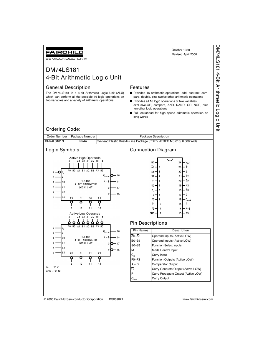
The DM74LS181 is a 4-bit Arithmetic Logic Unit (ALU)
which can perform all the possible 16 logic operations on
two variables and a variety of arithmetic operations.
October 1988
Revised April 2000
Features
n Provides 16 arithmetic operations: add, subtract, com-
pare, double, plus twelve other arithmetic operations
n Provides all 16 logic operations of two variables:
exclusive-OR, compare, AND, NAND, OR, NOR, plus
ten other logic operations
n Full lookahead for high speed arithmetic operation on
long words
Ordering Code:
Order Number Package Number
Package Description
DM74LS181N
N24A
24-Lead Plastic Dual-In-Line Package (PDIP), JEDEC MS-010, 0.600 Wide
Logic Symbols
Connection Diagram
Active High Operands
Active Low Operands
VCC = Pin 24
GND = Pin 12
Pin Descriptions
Pin Names
Description
A0–A3
B0–B3
S0–S3
M
Cn
F0–F3
A = B
G
P
Cn+4
Operand Inputs (Active LOW)
Operand Inputs (Active LOW)
Function Select Inputs
Mode Control Input
Carry Input
Function Outputs (Active LOW)
Comparator Output
Carry Generate Output (Active LOW)
Carry Propagate Output (Active LOW)
Carry Output
© 2000 Fairchild Semiconductor Corporation
DS009821
www.fairchildsemi.com
�
1
8
1
S
L
4
7
M
D
Functional Description
The DM74LS181 is a 4-bit high speed parallel Arithmetic
Logic Unit (ALU). Controlled by the four Function Select
inputs (S0–S3) and the Mode Control input (M), it can per-
form all the 16 possible logic operations or 16 different
arithmetic operations on active HIGH or active LOW oper-
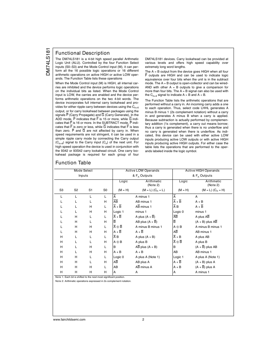
ands. The Function Table lists these operations
When the Mode Control input (M) is HIGH, all internal car-
ries are inhibited and the device performs logic operations
on the individual bits as listed. When the Mode Control
input is LOW, the carries are enabled and the device per-
forms arithmetic operations on the two 4-bit words. The
device incorporates full internal carry lookahead and pro-
vides for either ripple carry between devices using the Cn+4
output, or for carry lookahead between packages using the
signals P (Carry Propagate) and G (Carry Generate). In the
ADD mode, P indicates that F is 15 or more, while G indi-
cates that F is 16 or more. In the SUBTRACT mode, P indi-
cates that F is zero or less, while G indicates that F is less
than zero. P and G are not affected by carry in. When
speed requirements are not stringent, it can be used in a
simple ripple carry mode by connecting the Carry output
(Cn+4) signal to the Carry input (Cn) of the next unit. For
high speed operation the device is used in conjunction with
the 9342 or 93S42 carry lookahead circuit. One carry loo-
kahead package is required for each group of four
DM74LS181 devices. Carry lookahead can be provided at
various levels and offers high speed capability over
extremely long word lengths.
The A = B output from the device goes HIGH when all four
F outputs are HIGH and can be used to indicate logic
equivalence over four bits when the unit is in the subtract
mode. The A = B output is open-collector and can be wired-
AND with other A = B outputs to give a comparison for
more than four bits. The A = B signal can also be used with
the Cn+4 signal to indicate A > B and A < B.
The Function Table lists the arithmetic operations that are
performed without a carry in. An incoming carry adds a one
to each operation. Thus, select code LHHL generates A
minus B minus 1 (2s complement notation) without a carry
in and generates A minus B when a carry is applied.
Because subtraction is actually performed by complemen-
tary addition (1s complement), a carry out means borrow;
thus a carry is generated when there is no underflow and
no carry is generated when there is underflow. As indi-
cated, this device can be used with either active LOW
inputs producing active LOW outputs or with active HIGH
inputs producing active HIGH outputs. For either case the
table lists the operations that are performed to the oper-
ands labeled inside the logic symbol.
Function Table
Mode Select
Inputs
S3
S2
S1
S0
Active LOW Operands
Active HIGH Operands
& Fn Outputs
& Fn Outputs
Logic
(M = H)
Arithmetic
(Note 2)
(M = L) (Cn = L)
Logic
(M = H)
Arithmetic
(Note 2)
(M = L) (Cn = H)
L
L
L
L
L
L
L
L
H
H
H
H
H
H
H
H
L
L
L
L
H
H
H
H
L
L
L
L
H
H
H
H
L
L
H
H
L
L
H
H
L
L
H
H
L
L
H
H
L
H
L
H
L
H
L
H
L
H
L
H
L
H
L
H
A
AB
A + B
Logic 1
A + B
B
A ¯
B
A + B
A B
A ¯
B
A + B
Logic 0
AB
AB
A
B
A minus 1
AB minus 1
AB minus 1
minus 1
A plus (A + B)
AB plus (A + B)
A minus B minus 1
A + B
A plus (A + B)
A plus B
AB plus (A + B)
A + B
A plus A (Note 1)
AB plus A
AB minus A
A
B
A
A + B
A B
Logic 0
AB
B
A ¯
AB
A + B
A ¯
B
B
AB
Logic 1
A + B
A + B
A
A
A + B
A + B
minus 1
A plus AB
(A + B) plus AB
A minus B minus 1
AB minus 1
A plus AB
A plus B
(A + B) plus AB
AB minus 1
A plus A (Note 1)
(A + B) plus A
(A + B) plus A
A minus 1
Note 1: Each bit is shifted to the next most significant position.
Note 2: Arithmetic operations expressed in 2s complement notation.
www.fairchildsemi.com
2
�
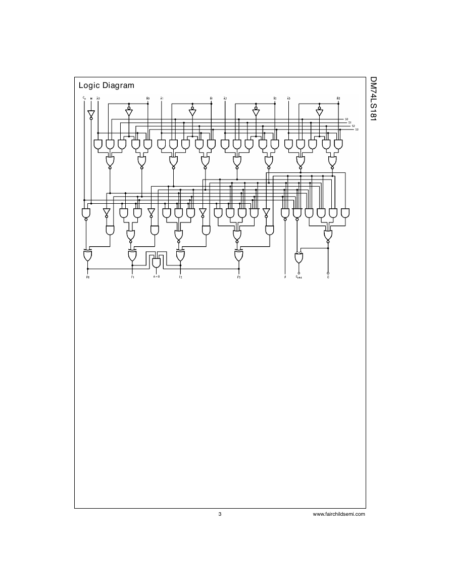
Logic Diagram
D
M
7
4
L
S
1
8
1
3
www.fairchildsemi.com
�
1
8
1
S
L
4
7
M
D
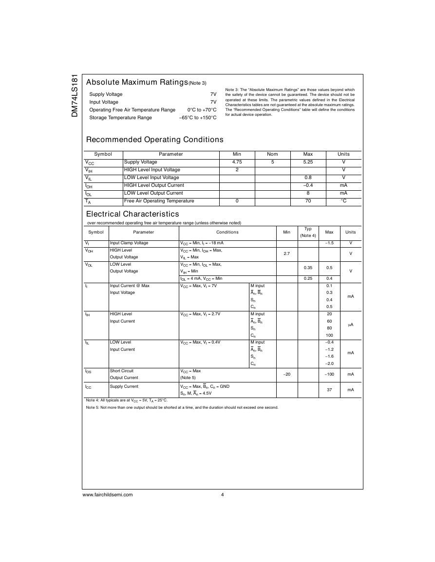
Absolute Maximum Ratings(Note 3)
Supply Voltage
Input Voltage
Operating Free Air Temperature Range
Storage Temperature Range
7V
7V
0 C to +70 C
- 65 C to +150 C
Note 3: The “Absolute Maximum Ratings” are those values beyond which
the safety of the device cannot be guaranteed. The device should not be
operated at these limits. The parametric values defined in the Electrical
Characteristics tables are not guaranteed at the absolute maximum ratings.
The “Recommended Operating Conditions” table will define the conditions
for actual device operation.
Recommended Operating Conditions
Symbol
Parameter
Min
4.75
2
Supply Voltage
HIGH Level Input Voltage
LOW Level Input Voltage
HIGH Level Output Current
LOW Level Output Current
Free Air Operating Temperature
VCC
VIH
VIL
IOH
IOL
TA
Electrical Characteristics
over recommended operating free air temperature range (unless otherwise noted)
0
Symbol
Parameter
Conditions
VI
VOH
VOL
II
IIH
IIL
IOS
ICC
Input Clamp Voltage
HIGH Level
Output Voltage
LOW Level
Output Voltage
Input Current @ Max
Input Voltage
HIGH Level
Input Current
LOW Level
Input Current
Short Circuit
Output Current
Supply Current
VCC = Min, II = - 18 mA
VCC = Min, IOH = Max,
VIL = Max
VCC = Min, IOL = Max,
VIH = Min
IOL = 4 mA, VCC = Min
VCC = Max, VI = 7V
VCC = Max, VI = 2.7V
VCC = Max, VI = 0.4V
VCC = Max
(Note 5)
VCC = Max, Bn, Cn = GND
Sn, M, An = 4.5V
Max
5.25
0.8
- 0.4
8
70
Typ
(Note 4)
0.35
0.25
Nom
5
Min
2.7
- 20
M input
An, Bn
Sn
Cn
M input
An, Bn
Sn
Cn
M input
An, Bn
Sn
Cn
Units
V
V
V
mA
mA
C
Max
- 1.5
0.5
0.4
0.1
0.3
0.4
0.5
20
60
80
100
- 0.4
- 1.2
- 1.6
- 2.0
- 100
37
Units
V
V
V
mA
m A
mA
mA
mA
Note 4: All typicals are at VCC = 5V, TA = 25 C.
Note 5: Not more than one output should be shorted at a time, and the duration should not exceed one second.
www.fairchildsemi.com
4
�
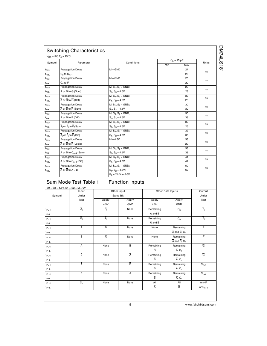
Switching Characteristics
VCC = 5V, TA = 25 C
Symbol
Parameter
Conditions
CL = 15 pF
Min
Max
27
20
26
20
29
23
32
26
30
30
30
33
32
25
32
33
33
29
38
38
41
41
50
62
M = GND
M = GND
M, S1, S2 = GND;
S1, S3 = 4.5V
M, S0, S3 = GND;
S1, S2 = 4.5V
M, S1, S2 = GND;
S0, S3 = 4.5V
M, S0, S3 = GND;
S1, S2 = 4.5V
M, S1, S2 = GND;
S0, S3 = 4.5V
M, S0, S3 = GND;
S1, S2 = 4.5V
M = 4.5V
M, S1, S2 = GND;
S0, S3 = 4.5V
M, S0, S3 = GND;
S1, S2 = 4.5V
M, S0, S3 = GND;
S1, S2 = 4.5V;
RL = 2 kW
Function Inputs
to 5.0V
Other Input
Same Bit
Other Data Inputs
tPLH
tPHL
tPLH
tPHL
tPLH
tPHL
tPLH
tPHL
tPLH
tPHL
tPLH
tPHL
tPLH
tPHL
tPLH
tPHL
tPLH
tPHL
tPLH
tPHL
tPLH
tPHL
tPLH
tPHL
Propagation Delay
Cn to Cn+4
Propagation Delay
Cn to F
Propagation Delay
A or B to G (Sum)
Propagation Delay
A or B to G (Diff)
Propagation Delay
A or B to P (Sum)
Propagation Delay
A or B to P (Diff)
Propagation Delay
Ai or Bi to Fi(Sum)
Propagation Delay
Ai or Bi to Fi(Diff)
Propagation Delay
A or B to F (Logic)
Propagation Delay
A or B to Cn+4 (Sum)
Propagation Delay
A or B to Cn+4 (Diff)
Propagation Delay
A or B to A = B
Sum Mode Test Table 1
S0 = S3 = 4.5V, S1 = S2 = M = 0V
Input
Under
Test
Symbol
tPLH
tPHL
tPLH
tPHL
tPLH
tPHL
tPLH
tPHL
tPLH
tPHL
tPLH
tPHL
tPLH
tPHL
tPLH
tPHL
tPLH
tPHL
Ai
Bi
A
B
A
B
A
B
Cn
D
M
7
4
L
S
1
8
1
Units
ns
ns
ns
ns
ns
ns
ns
ns
ns
ns
ns
ns
Output
Under
Test
Fi
Fi
P
P
G
G
Cn+4
Cn+4
Any F
or Cn+4
Apply
4.5V
Remaining
A and B
Remaining
A and B
None
None
Remaining
B
Apply
GND
Cn
Cn
Remaining
A and B, Cn
Remaining
A and B, Cn
Remaining
A, Cn
Remaining
Remaining
B
A, Cn
Remaining
Remaining
B
A, Cn
Remaining
Remaining
B
All
A
A, Cn
All
B
Apply
4.5V
Bi
Ai
B
A
None
None
None
None
None
Apply
GND
None
None
None
None
B
A
B
A
None
5
www.fairchildsemi.com
�
1
8
1
S
L
4
7
M
D
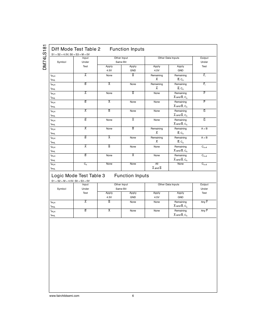
Diff Mode Test Table 2
S1 = S2 = 4.5V, S0 = S3 = M = 0V
Input
Under
Test
Symbol
A
B
A
A
B
B
A
tPLH
tPHL
tPLH
tPHL
tPLH
tPHL
tPLH
tPHL
tPLH
tPHL
tPLH
tPHL
tPLH
tPHL
tPLH
tPHL
tPLH
tPHL
tPLH
tPHL
tPLH
tPHL
Logic Mode Test Table 3
S1 = S2 = M = 4.5V, S0 = S3 = 0V
Input
Under
Test
Symbol
Cn
B
A
B
tPLH
tPHL
tPLH
tPHL
A
B
Function Inputs
Other Input
Same Bit
Apply
GND
B
Other Data Inputs
Apply
4.5V
Apply
GND
Remaining
Remaining
A
B, Cn
None
Remaining
Remaining
B
None
None
A
B
None
None
A
None
A
None
None
None
None
Remaining
A
B, Cn
Remaining
A and B, Cn
Remaining
A and B, Cn
Remaining
A and B, Cn
Remaining
A and B, Cn
Remaining
B, Cn
Remaining
Remaining
A
None
None
All
A and B
B, Cn
Remaining
A and B, Cn
Remaining
A and B, Cn
None
Function Inputs
Other Input
Same Bit
Other Data Inputs
Apply
GND
None
None
Apply
4.5V
None
None
Apply
GND
Remaining
A and B, Cn
Remaining
A and B, Cn
Apply
4.5V
None
A
None
A
B
None
None
A
B
None
None
Apply
4.5V
B
A
Output
Under
Test
Fi
Fi
P
P
G
G
A = B
A = B
Cn+4
Cn+4
Cn+4
Output
Under
Test
Any F
Any F
www.fairchildsemi.com
6
�
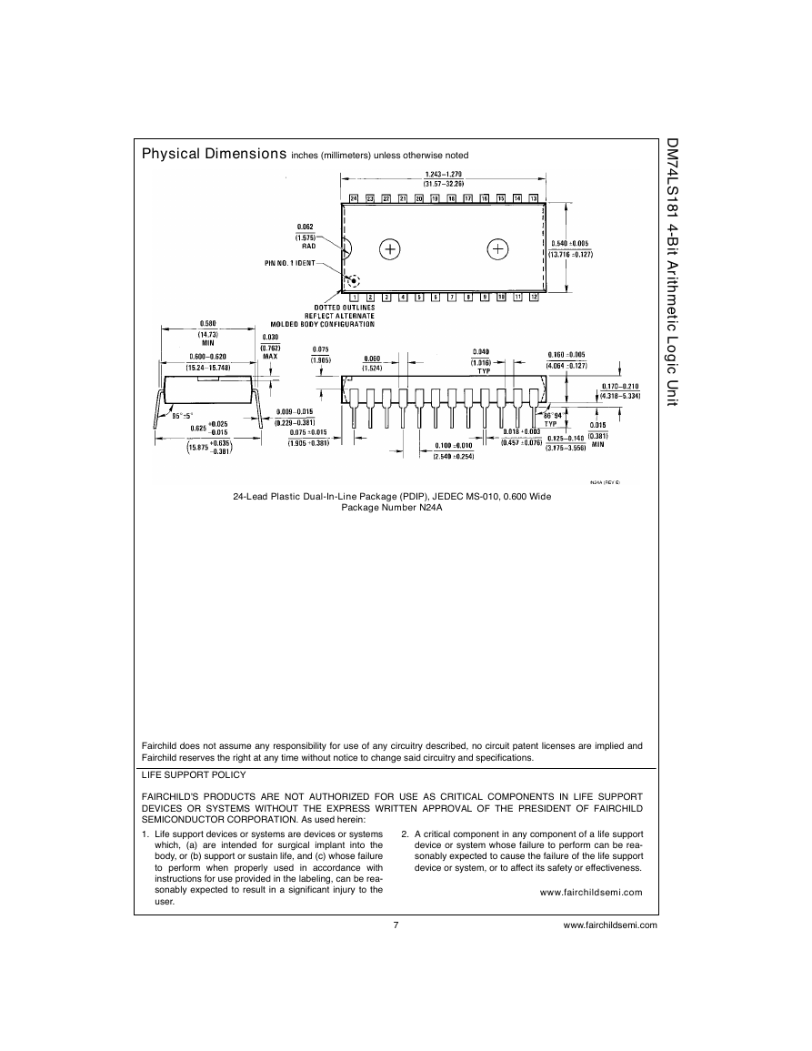
Physical Dimensions inches (millimeters) unless otherwise noted
D
M
7
4
L
S
1
8
1
4
-
B
i
t
A
r
i
t
h
m
e
t
i
c
L
o
g
c
U
n
i
t
i
24-Lead Plastic Dual-In-Line Package (PDIP), JEDEC MS-010, 0.600 Wide
Package Number N24A
Fairchild does not assume any responsibility for use of any circuitry described, no circuit patent licenses are implied and
Fairchild reserves the right at any time without notice to change said circuitry and specifications.
LIFE SUPPORT POLICY
FAIRCHILD’S PRODUCTS ARE NOT AUTHORIZED FOR USE AS CRITICAL COMPONENTS IN LIFE SUPPORT
DEVICES OR SYSTEMS WITHOUT THE EXPRESS WRITTEN APPROVAL OF THE PRESIDENT OF FAIRCHILD
SEMICONDUCTOR CORPORATION. As used herein:
1. Life support devices or systems are devices or systems
which, (a) are intended for surgical implant into the
body, or (b) support or sustain life, and (c) whose failure
to perform when properly used in accordance with
instructions for use provided in the labeling, can be rea-
sonably expected to result in a significant injury to the
user.
2. A critical component in any component of a life support
device or system whose failure to perform can be rea-
sonably expected to cause the failure of the life support
device or system, or to affect its safety or effectiveness.
www.fairchildsemi.com
7
www.fairchildsemi.com
�


 2023年江西萍乡中考道德与法治真题及答案.doc
 2012年重庆南川中考生物真题及答案.doc
 2013年江西师范大学地理学综合及文艺理论基础考研真题.doc
 2020年四川甘孜小升初语文真题及答案I卷.doc
 2020年注册岩土工程师专业基础考试真题及答案.doc
 2023-2024学年福建省厦门市九年级上学期数学月考试题及答案.doc
 2021-2022学年辽宁省沈阳市大东区九年级上学期语文期末试题及答案.doc
 2022-2023学年北京东城区初三第一学期物理期末试卷及答案.doc
 2018上半年江西教师资格初中地理学科知识与教学能力真题及答案.doc
 2012年河北国家公务员申论考试真题及答案-省级.doc
 2020-2021学年江苏省扬州市江都区邵樊片九年级上学期数学第一次质量检测试题及答案.doc
 2022下半年黑龙江教师资格证中学综合素质真题及答案.doc