ATA-ATAPI-7-1.pdf
Points of Contact:
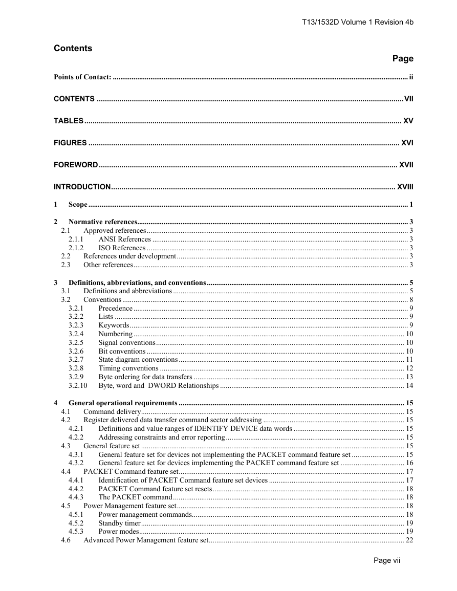
Contents
Tables
Figures
Foreword
Introduction
Scope
Figure 1 - ATA document relationships
Table 1 - PACKET delivered command sets
Normative references
Approved references
ANSI References
ISO References
References under development
Other references
Definitions, abbreviations, and conventions
Definitions and abbreviations
Conventions
Precedence
Lists
Keywords
Numbering
Signal conventions
Bit conventions
State diagram conventions
Figure 2 - State diagram convention
Timing conventions
Byte ordering for data transfers
Table 2 - Byte order
Table 3 - Byte order
Byte, word and DWORD Relationships
Figure 3 - Byte, word and DWORD relationships
General operational requirements
Command delivery
Register delivered data transfer command sector addressing
Definitions and value ranges of IDENTIFY DEVICE data words
Addressing constraints and error reporting
General feature set
General feature set for devices not implementing the PACKET
General feature set for devices implementing the PACKET comm
PACKET Command feature set
Identification of PACKET Command feature set devices
PACKET Command feature set resets
The PACKET command
Power Management feature set
Power management commands
Standby timer
Power modes
Figure 4 - Power management state diagram
Advanced Power Management feature set
Security Mode feature set
Security mode initial setting
User password lost
Attempt limit for SECURITY UNLOCK command
Security mode states
Figure 5 - Security mode state diagram
Table 4 - Security mode command actions
SMART (Self-monitoring, analysis, and reporting technology)
Device SMART data structure
On-line data collection
Off-line data collection
Threshold exceeded condition
SMART feature set commands
SMART operation with power management modes
SMART device error log reporting
Host Protected Area feature set
BIOS determination of SET MAX security exension status
BIOS locking SET MAX
Figure 6 - SET MAX security state diagram
CompactFlash( Association (CFA) feature set
Removable Media Status Notification and Removable Media feat
Removable Media Status Notification feature set
Removable Media feature set
Power-Up In Standby feature set
Automatic Acoustic Management (AAM) feature set
48-bit Address feature set
Table 5 - 48-bit addresses
Table 6 - 28-bit addresses
Device Configuration Overlay feature set
Figure 7 - Device Configuration Overlay state diagram
Media Card Pass Through Command feature set
Table 7 - Media Card type references
Streaming feature set
Streaming commands
Urgent bit
Flush to Disk bit
Not Sequential bit
Read Continuous bit
Write Continuous bit
Handle Streaming Error bit
Streaming Logs
General Purpose Logging feature set
Overlapped feature set
Queued feature set
Long Physical Sector Feature Set for Non-Packet Devices
Figure 8 - Long Logical and long Physical Sector Example
Long Logical Sector Feature Set for Non-Packet Devices
Table 8 - Long Logical Sector Function
Devices Implementing the Long Physical Sector Feature Set an
I/O register descriptions
Overview
Table 9 - I/O registers
Alternate Status register
Command register
Data port
Data register
Device register
Device Control register
Error register
Features register
LBA High/Byte Count High register
LBA Low register
LBA Mid/Byte Count Low register
Sector Count/Interrupt Reason register
Status register
Direction
Access restrictions
Effect
Functional description
Field/bit description
BSY (Busy)
DRDY (Device ready)
DF/SE (Device Fault / Stream Error)
Command dependent
DRQ (Data request)
Obsolete bits
ERR / CHK (Error / Check)
Signature and persistence
Signature for devices not implementing the PACKET command fe
Signature for devices implementing the PACKET command featur
Reserved Signatures for Serial ATA Working Groups
Single device configurations
Device 0 only configurations
Device 1 only configurations
Command Descriptions
Overview
CFA ERASE SECTORS
CFA REQUEST EXTENDED ERROR CODE
Table 10 - Extended error codes
CFA TRANSLATE SECTOR
Table 11 - CFA TRANSLATE SECTOR Information
CFA WRITE MULTIPLE WITHOUT ERASE
CFA WRITE SECTORS WITHOUT ERASE
CHECK MEDIA CARD TYPE
CHECK POWER MODE
CONFIGURE STREAM
DEVICE CONFIGURATION
Table 12 - Device Configuration Overlay Features register va
DEVICE CONFIGURATION RESTORE
DEVICE CONFIGURATION FREEZE LOCK
DEVICE CONFIGURATION IDENTIFY
Table 13 - Device Configuration Identify data structure
DEVICE CONFIGURATION SET
Table 14 - Device Configuration Overlay data structure
DEVICE RESET
DOWNLOAD MICROCODE
EXECUTE DEVICE DIAGNOSTIC
Table 15 - Diagnostic codes
FLUSH CACHE
FLUSH CACHE EXT
GET MEDIA STATUS
IDENTIFY DEVICE
Table 16 - IDENTIFY DEVICE data
Word 0: General configuration
Word 1: Obsolete
Word 2: Specific configuration.
Word 3: Obsolete
Word (5:4): Retired.
Word 6: Obsolete
Words (8:7): Reserved for assignment by the CompactFlash( Association
Word 9: Retired.
Words (19:10): Serial number
Word (21:20): Retired.
Word 22: Obsolete.
Word (26:23): Firmware revision
Words (46:27): Model number
Word 47: READ/WRITE MULTIPLE support.
Word 48: Reserved.
Word (50:49): Capabilities
Words (52:51): Obsolete
Word 53: Field validity
Word (58:54): Obsolete
Word 59: Multiple sector setting
Word (61:60): Total number of user addressable sectors
Word 62: Obsolete
Word 63: Multiword DMA transfer
Word 64: PIO transfer modes supported
Word 65: Minimum Multiword DMA transfer cycle time per word
Word 66: Device recommended Multiword DMA cycle time
Word 67: Minimum PIO transfer cycle time without IORDY flow
Word 68: Minimum PIO transfer cycle time with IORDY flow con
Words (74:69): Reserved
Word 75: Queue depth
Words (79:76): Reserved for Serial ATA
Word 80: Major version number
Word 81: Minor version number
Table 17 - Minor version number
Words (84:82): Features/command sets supported
Words (87:85): Features/command sets enabled
Word 88: Ultra DMA modes
Word 89: Time required for Security erase unit completion
Word 90: Time required for Enhanced security erase unit comp
Word 91: Advanced power management level value
Word 92: Master Password Revision Code
Word 93: Hardware configuration test results
Word 94: Current automatic acoustic management value
Word 95: Stream Minimum Request Size
Word 96: Streaming Transfer Time -- DMA
Word 97: Streaming Access Latency - DMA and PIO
Words (99:98): Streaming Performance Granularity
Words (103:100): Maximum user LBA for 48-bit Address feature
Word 104: Streaming Transfer Time - PIO
Word 106: Physical sector size / Logical Sector Size
Word 107: Inter-seek delay for ISO 7779 standard acoustic te
Words (111:108): World wide name
Words (115:112): Reserved for a 128-bit world wide name
Word 116: Reserved for technical report.
Words 117-118: Logical Sector Size
Words (126:119): Reserved
Word 127: Removable Media Status Notification feature set su
Word 128: Security status
Words (159:129): Vendor specific.
Word 160: CFA power mode
Words (175:161): Reserved for assignment by the CompactFlash( Association
Words (205:176): Current media serial number
Words (254:206): Reserved.
Word 255: Integrity word
IDENTIFY PACKET DEVICE
Table 18 - IDENTIFY PACKET DEVICE data
Word 0: General configuration
Word 1: Reserved
Word 2: Specific configuration
Words (9:3): Reserved
Words (19:10): Serial number
Words (22:20): Reserved
Words (26:23): Firmware revision
Words (46:27): Model number
Words (48:47): Reserved
Word 49: Capabilities
Word 50: Capabilities
Word 51: Obsolete
Word 52: Reserved
Word 53: Field validity
Words (61:54): Reserved
Word 62: DMADIR
Word 63: Multiword DMA transfer
Word 64: PIO transfer mode supported
Word 65: Minimum multiword DMA transfer cycle time per word
Word 66: Device recommended multiword DMA cycle time
Word 67: Minimum PIO transfer cycle time without flow contro
Word 68: Minimum PIO transfer cycle time with IORDY
Word (70:69): Reserved
Word 71: PACKET to bus release time
Word 72: SERVICE to bus release time
Word (74:73): Reserved
Word 75: Queue depth
Words (79:76): Reserved for Serial ATA
Word 80: Major revision number
Word 81: Minor revision number
Words (84:82): Features/command sets supported
Words (87:85): Features/command sets enabled
Word 88:Ultra DMA modes
Word 89: Time required for Security erase unit completion
Word 90: Time required for Enhanced security erase unit comp
Word (92:91): Reserved
Word 93: Hardware reset results
Word 94: Current automatic acoustic management value
Word (124:95): Reserved
Word 125 ATAPI byte count=0 behavior.
Word 126: Obsolete
Word 127: Removable Media Status Notification feature set su
Word 128: Security status
Words (160:129): Reserved
Words (175:161): Reserved for assignment by the CompactFlash( Association
Words (254:176): Reserved
Word 255: Integrity Word
IDLE
Table 19 - Automatic Standby timer periods
IDLE IMMEDIATE
MEDIA EJECT
MEDIA LOCK
MEDIA UNLOCK
NOP
PACKET
READ BUFFER
READ DMA
READ DMA EXT
READ DMA QUEUED
READ DMA QUEUED EXT
READ LOG EXT
Command code
Feature set
Protocol
Inputs
Table 20 - Log address definition
Normal outputs
Error outputs
Prerequisites
Description
General Purpose Log Directory
Table 21 - General Purpose Log Directory
Extended Comprehensive SMART Error log
Table 22 - Extended Comprehensive SMART error log
Table 23 - Extended Error log data structure
Table 24 - Command data structure
Table 25 - Error data structure
Table 26 - State field values
Extended Self-test log sector
Table 27 - Extended Self-test log data structure
Table 28 - Extended Self-test log descriptor entry
Read Stream Error Log
Table 29 - Read Stream Error Log
Table 30 - Error Log Entry
Write Stream Error Log
Table 31 - Write Stream Error Log
Streaming Performance Log
Table 32 - Streaming Performance Parameters Log
Table 33 - Sector Time Array Entry (Linearly Interpolated)
Table 34 - Position Array Entry (Linearly Interpolated)
Table 35 - Access Time Array Entry (Linearly Interpolated)
Delayed LBA Log
Table 36 - Delayed LBA log
READ MULTIPLE
READ MULTIPLE EXT
READ NATIVE MAX ADDRESS
READ NATIVE MAX ADDRESS EXT
READ SECTOR(S)
READ SECTOR(S) EXT
READ STREAM DMA EXT
READ STREAM EXT
READ VERIFY SECTOR(S)
READ VERIFY SECTOR(S) EXT
SECURITY DISABLE PASSWORD
Table 37 - Security password content
SECURITY ERASE PREPARE
SECURITY ERASE UNIT
Table 38 - SECURITY ERASE UNIT password
SECURITY FREEZE LOCK
SECURITY SET PASSWORD
Table 39 - SECURITY SET PASSWORD data content
Table 40 - Identifier and security level bit interaction
SECURITY UNLOCK
SERVICE
SET FEATURES
Command code
Feature set
Protocol
Inputs
Normal outputs
Error outputs
Prerequisites
Description
Table 41 - SET FEATURES register definitions
Enable/disable 8-bit PIO data transfer
Enable/disable write cache
Set transfer mode
Table 42 - Transfer mode values
Enable/disable advanced power management
Table 43 - Advanced power management levels
Enable/disable Power-Up In Standby feature set
Enable/disable CFA power mode 1
Power-Up In Standby feature set device spin-up
Enable/disable Media Status Notification
Enable/disable Automatic Acoustic Management
Table 44 - Automatic acoustic management levels
Set Maximum Host Interface Sector Times
Enable/disable read look-ahead
Enable/disable release interrupt
Enable/disable SERVICE interrupt
Enable/disable reverting to defaults
SET MAX
Table 45 - SET MAX Features register values
SET MAX ADDRESS
SET MAX SET PASSWORD
Table 46 - SET MAX SET PASSWORD data content
SET MAX LOCK
SET MAX UNLOCK
SET MAX FREEZE LOCK
SET MAX ADDRESS EXT
SET MULTIPLE MODE
SLEEP
SMART
Table 47 - SMART Feature register values
SMART DISABLE OPERATIONS
SMART ENABLE/DISABLE ATTRIBUTE AUTOSAVE
SMART ENABLE OPERATIONS
SMART EXECUTE OFF-LINE IMMEDIATE
Table 48 - SMART EXECUTE OFF-LINE IMMEDIATE LBA Low register
Figure 9 - Selective self-test test span example
SMART READ DATA
Table 49 - Device SMART data structure
Table 50 - Off-line data collection status byte values
Table 51 - Self-test execution status values
SMART READ LOG
Table 52 - Log address definition
Table 53 - SMART Log Directory
Table 54 - SMART summary error log sector
Table 55 - Error log data structure
Table 56 - Command data structure
Table 57 - Error data structure
Table 58 - State field values
Table 59 - Comprehensive error log
Table 60 - Self-test log data structure
Table 61 - Self-test log descriptor entry
Table 62 - Selective self-test log
Table 63 - Selective self-test feature flags
SMART RETURN STATUS
SMART WRITE LOG
STANDBY
STANDBY IMMEDIATE
WRITE BUFFER
WRITE DMA
WRITE DMA EXT
WRITE DMA FUA EXT
WRITE DMA QUEUED
WRITE DMA QUEUED EXT
WRITE DMA QUEUED FUA EXT
WRITE LOG EXT
WRITE MULTIPLE
WRITE MULTIPLE EXT
WRITE MULTIPLE FUA EXT
WRITE SECTOR(S)
WRITE SECTOR(S) EXT
WRITE STREAM DMA EXT
WRITE STREAM EXT
Parallel interface physical and electrical requirements (See
Parallel interface signal assignments and descriptions (See
Parallel interface general operating requirements of the phy
Parallel interface register addressing (See Volume 2)
Parallel interface transport Protocols (See Volume 2)
Parallel interface timing (See Volume 2)
Serial interface overview (See Volume 3)
Serial interface physical layer (See Volume 3)
Serial interface link layer (See Volume 3)
Serial interface transport layer (See Volume 3)
Serial interface device command layer (See Volume 3)
Host command layer (See Volume 3)
Serial interface host adapter register interface (See Volume
Serial interface error handling (See Volume 3)
BIBLIOGRAPHY (INFORMATIVE)
COMMAND SET SUMMARY (INFORMATIVE)
Table 64 - Command Matrix
Table 65 - Command codes (sorted by command code)
Table 66- Command codes (sorted by command)
DESIGN AND PROGRAMMING CONSIDERATIONS FOR LARGE PHYSICAL SEC
Introduction
Physical sectors
Unaligned write
Figure 10 - Unaligned Write Example
SET MAX
Software compatibility
DEVICE DETERMINATION OF CABLE TYPE (INFORMATIVE) (SEE VOLUME
SIGNAL INTEGRITY AND UDMA GUIDE (INFORMATIVE) (SEE VOLUME 2)
REGISTER SELECTION ADDRESS SUMMARY (INFORMATIVE) (SEE VOLUME
SAMPLE CODE FOR CRC AND SCRAMBLING (INFORMATIVE) (SEE VOLUME
FIS TYPE FIELD VALUE SELECTION (INFORMATIVE) (SEE VOLUME 3)
PHYSICAL LAYER IMPLEMENTATION EXAMPLES (INFORMATIVE) (SEE VO
COMMAND PROCESSING EXAMPLE (INFORMATIVE) (SEE VOLUME 3)
ATA-ATAPI-7-2
Points of Contact:
Contents
Page
Foreword
Introduction
Scope
Figure 1 ( ATA document relationships
Table 1 ( PACKET delivered command sets
Normative references
Approved references
ANSI References
ISO References
References under development
Other references
Definitions, abbreviations, and conventions
Definitions and abbreviations
Conventions
Precedence
Lists
Keywords
Numbering
Signal conventions
Bit conventions
State diagram conventions
Figure 2 ( State diagram convention
Timing conventions
Byte ordering for data transfers
Table 2 ( Byte order
Table 3 ( Byte order
Byte, word and DWORD Relationships
Figure 3 - Byte, word and DWORD relationships
General command operational requirements (See Volume 1)
Interface register descriptions (See Volume 1)
Command descriptions (See Volume 1)
Parallel interface physical and electrical requirements
Cable configuration
Electrical characteristics
Table 4 ( DC characteristics
Table 5 ( AC characteristics
AC characteristics measurement techniques
Slew rate
VSSO
Driver types and required termination
Table 6 ( Driver types and required termination
Electrical characteristics for Ultra DMA
Cable configuration
Series termination required for Ultra DMA
Table 7 ( Typical series termination for Ultra DMA
Figure 4 ( Ultra DMA termination with pull-up or pull-down
PCB trace requirements for Ultra DMA
Connectors and cable asemblies
40-pin Connector
Figure 5 ( Host or device 40-pin I/O header
Table 8 ( Host or device 40-pin I/O header
Figure 6 ( 40-pin I/O cable connector
Table 9 ( 40-pin I/O cable connector
Table 10 ( 40-pin I/O connector interface signals
Figure 7 ( 40-pin I/O header mounting
40-conductor cable
Figure 8 ( 40-conductor cable configuration
Table 11 ( 40-conductor cable configuration
80-conductor cable assembly using the 40-pin connector
Table 12 ( 80-conductor cable electrical requirements
Figure 9 ( 80-conductor ribbon cable
Table 13 ( 80-conductor ribbon cable
Figure 10 ( 80-conductor cable configuration
Table 14 ( 80-conductor cable configuration
Table 15 ( Signal assignments for connectors grounding even conductors
Table 16 ( Signal assignments for connectors grounding odd conductors
Figure 11 ( Connector labeling for even or odd conductor grounding
4-pin power connector
Figure 12 ( Device 4-pin power header
Table 17 ( Device 4-pin power header
Figure 13 ( 4-pin power cable connector
Table 18 ( 4-pin power cable connector
Table 19 ( 4-pin power connector pin assignments
Mating performance
Unitized connectors
Figure 14 ( Unitized connector
Table 20 ( Unitized connector
Figure 15 ( Unitized connector
Table 21 ( Unitized connector
50-pin 2.5 inch form factor style connector
Figure 16 ( 50-pin 2.5 inch form factor style connector
Table 22 ( 50-pin connector
Table 23 ( Signal assignments for 50-pin 2.5 inch form factor style connector
68-pin PCMCIA connector
Signals
Signal descriptions
Table 24 ( Signal assignments for 68-pin connector
Removability considerations
CompactFlash( connector
1.8 inch 3.3V parallel connector
Figure 17 ( 1.8 inch 3.3V parallel connector
Table 25 ( 1.8 inch 3.3V parallel connector
Figure 18 ( 1.8 inch 3.3 V parallel host connector
Table 26 ( 1.8 inch 3.3 V parallel host connector
Table 27 ( Pin assignments for the 1.8 inch 3.3V parallel connector
Physical form factors
3.5” form factor
Figure 19 \( 3.5” form factor
Table 28 \( 3.5” form factor
Connector location for 3.5” form factor
2.5” form factor
Figure 20 \( 2.5” form factor
Table 29 \( 2.5“ form factor
Figure 21 \(2.5” form factor mounting ho�
Connector location for 2.5” form factor
Figure 22 \( 2.5” form factor connector �
Table 30 ( 2.5 inch form factor connector location
1.8” PCMCIA form factor
Connector location for 1.8” PCMCIA form factor
1.8” 5V parallel form factor
Figure 23 ( 1.8 inch 5V parallel form factor
Table 31 ( 1.8 inch 5V parallel form factor
Connector location for 1.8” 5V parallel form factor
Figure 24 ( 1.8 inch 5V parallel form factor connector location
Table 32 ( 1.8 inch 5V parallel form factor connector location
1.8” 3.3V parallel form factor
Figure 25 ( 1.8 inch 3.3V parallel form factor
Table 33 ( 1.8 inch 3.3V parallel form factor
Connector location for 1.8” 3.3V parallel form factor
5.25” form factor
5.25” HDD form factor
Figure 26 ( 5.25 inch HDD form factor
Table 34 ( 5.25 inch HDD form factor
5.25 inch CD-ROM form factor
Figure 27 ( 5.25 inch CD-ROM form factor
Table 35 ( 5.25 inch CD-ROM form factor
Figure 28 ( 5.25 inch CD-ROM connector location
Parallel interface signal assignments and descriptions
Signal summary
Table 36 ( Interface signal name assignments
Signal descriptions
CS(1:0)- (Chip select)
DA(2:0) (Device address)
DASP- (Device active, device 1 present)
DD(15:0) (Device data)
DIOR-:HDMARDY-:HSTROBE (Device I/O read:Ultra DMA ready:Ultr
DIOW-:STOP (Device I/O write:Stop Ultra DMA burst)
DMACK- (DMA acknowledge)
DMARQ (DMA request)
INTRQ (Device interrupt)
IORDY:DDMARDY-:DSTROBE (I/O channel ready:Ultra DMA ready:Ul
PDIAG-:CBLID- (Passed diagnostics:Cable assembly type identi
Table 37 - Cable type identification
RESET- (Hardware reset)
CSEL (Cable select)
CSEL with 40-conductor cable
Figure 29 ( Cable select example
CSEL with 80-conductor cable
Figure 30 ( Alternate cable select example
Parallel interface general operational requirements
Interrupts
Multiword DMA
Ultra DMA feature set
Overview
Phases of operation
Ultra DMA burst initiation phase rules
Data transfer phase rules
Ultra DMA burst termination phase rules
Host determination of cable type by detecting CBLID-
Figure 31 - Example configuration of a system with a 40-cond
Figure 32 - Example configuration of a system where the host
Figure 33 - Example configuration of a system where the host
Table 38 - Host detection of CBLID-
Parallel interface register addressing
Table 39 ( I/O registers
Table 40 ( Device response to DIOW-/DIOR-
Table 41 ( Device is not selected, DMACK- is not asserted
Table 42 ( Device is selected, DMACK- is not asserted
Table 44 (Device 1 is selected and Device 0 is responding for Device 1
Table 45 ( Device is in Sleep mode, DEVICE RESET is not implemented, DMACK- is not asserted
Table 46 ( Device is in Sleep mode, DEVICE RESET is implemented, DMACK- is not asserted
Parallel interface transport protocol
Figure 34 ( Overall host protocol state sequence
Figure 35 ( Overall device protocol state sequence
Power-on and hardware reset protocol
Figure 36 ( Host power-on or hardware reset state diagram
Figure 37 ( Device power-on or hardware reset state diagram
Software reset protocol
Figure 38 ( Host software reset state diagram
Figure 39 ( Device 0 software reset state diagram
Figure 40 ( Device 1 software reset state diagram
Bus idle protocol
Figure 41 ( Host bus idle state diagram
Figure 42 ( Additional Host bus Idle state diagram with Overlap or overlap and queuing
Figure 43 ( Device bus Idle state diagram
Figure 44 ( Additional Device bus Idle state diagram with Overlap or overlap and queuing
Non-data command protocol
Figure 45 ( Host Non-Data state diagram
Figure 46 ( Device Non-Data state diagram
PIO data-in command protocol
Figure 47 ( Host PIO data-In state diagram
Figure 48 ( Device PIO data-In state diagram
PIO data-out command protocol
Figure 49 ( Host PIO data-Out state diagram
Figure 50 ( Device PIO data-Out state diagram
DMA command protocol
Figure 51 ( Host DMA state diagram
Figure 52 ( Device DMA state diagram
PACKET command protocol
Figure 53 ( Host PACKET non-data and PIO data command state diagram
Figure 54 ( Device PACKET non-data and PIO data command state diagram
Figure 55 ( Host PACKET DMA command state diagram
Figure 56 ( Device PACKET DMA command state diagram
READ/WRITE DMA QUEUED command protocol
Figure 57 ( Host DMA QUEUED state diagram
Figure 58 ( Device DMA QUEUED command state diagram
EXECUTE DEVICE DIAGNOSTIC command protocol
Figure 59 ( Host EXECUTE DEVICE DIAGNOSTIC state diagram
Figure 60 ( Device 0 EXECUTE DEVICE DIAGNOSTIC state diagram
Figure 61 ( Device 1 EXECUTE DEVICE DIAGNOSTIC command state diagram
DEVICE RESET command protocol
Figure 62 ( Host DEVICE RESET command state diagram
Figure 63 ( Device DEVICE RESET command state diagram
Ultra DMA data-in commands
Initiating an Ultra DMA data-in burst
The data-in transfer
Pausing an Ultra DMA data-in burst
Device pausing an Ultra DMA data-in burst
Host pausing an Ultra DMA data-in burst
Terminating an Ultra DMA data-in burst
Device terminating an Ultra DMA data-in burst
Host terminating an Ultra DMA data-in burst
Ultra DMA data-out commands
Initiating an Ultra DMA data-out burst
The data-out transfer
Pausing an Ultra DMA data-out burst
Host pausing an Ultra DMA data-out burst
Device pausing an Ultra DMA data-out burst
Terminating an Ultra DMA data-out burst
Host terminating an Ultra DMA data-out burst
Device terminating an Ultra DMA data-out burst
Ultra DMA CRC rules
Figure 64 ( Example Parallel CRC generator
Table 47 ( Equations for parallel generation of a CRC polynomial
Parallel interface timing
Deskewing
Transfer timing
Register transfers
Figure 65 ( Register transfer to/from device
Table 48 ( Register transfer to/from device
PIO data transfers
Figure 66 ( PIO data transfer to/from device
Table 49 ( PIO data transfer to/from device
Multiword DMA data transfer
Table 50 ( Multiword DMA data transfer
Initiating a Multiword DMA data burst
Figure 67 ( Initiating a Multiword DMA data burst
Sustaining a Multiword DMA data burst
Figure 68 - Sustaining a Multiword DMA data burst
Device terminating a Multiword DMA data burst
Figure 69 ( Device terminating a Multiword DMA data burst
Host terminating a Multiword DMA data burst
Figure 70 ( Host terminating a Multiword DMA data burst
Ultra DMA data transfer
Table 51 ( Ultra DMA data burst timing requirements
Table 52 ( Ultra DMA data burst timing descriptions
Name
Table 53 ( Ultra DMA sender and recipient IC timing requirements
Initiating an Ultra DMA data-in burst
Figure 71 ( Initiating an Ultra DMA data-in burst
Sustained Ultra DMA data-in burst
Figure 72 ( Sustained Ultra DMA data-in burst
Host pausing an Ultra DMA data-in burst
Figure 73 ( Host pausing an Ultra DMA data-in burst
Device terminating an Ultra DMA data-in burst
Figure 74 ( Device terminating an Ultra DMA data-in burst
Host terminating an Ultra DMA data-in burst
Figure 75 ( Host terminating an Ultra DMA data-in burst
Initiating an Ultra DMA data-out burst
Figure 76 ( Initiating an Ultra DMA data-out burst
Sustained Ultra DMA data-out burst
Figure 77 ( Sustained Ultra DMA data-out burst
Device pausing an Ultra DMA data-out burst
Figure 78 ( Device pausing an Ultra DMA data-out burst
Host terminating an Ultra DMA data-out burst
Figure 79 ( Host terminating an Ultra DMA data-out burst
Device terminating an Ultra DMA data-out burst
Figure 80 ( Device terminating an Ultra DMA data-out burst
Serial interface overview (See Volume 3)
Serial interface physical layer (See Volume 3)
Serial interface link layer (See Volume 3)
Serial interface transport layer (See Volume 3)
Serial interface device command layer (See Volume 3)
Host command layer (See Volume 3)
Serial interface host adapter register interface (See Volume
Serial interface error handling (See Volume 3)
BIBLIOGRAPHY (INFORMATIVE) (SEE VOLUME 1)
COMMAND SET SUMMARY (INFORMATIVE) (SEE VOLUME 1)
DESIGN AND PROGRAMMING CONSIDERTIONS FOR LARGE PHYSICAL SECT
DEVICE DETERMINATION OF CABLE TYPE (INFORMATIVE)
Overview
Sequence for device detection of installed capacitor
Figure 81 - Example configuration of a system where the devi
Table 54 - Device detection of installed capacitor
Table 55 - Results of device based cable detection if the h
Using the combination of methods for detecting cable type
Table 56 - Results of using both host and device cable detec
Table 57 - Results for all combinations of device and host c
SIGNAL INTEGRITY AND UDMA GUIDE (INFORMATIVE)
Introduction
The issues
Timing
Cabling
Skew
Source-terminated bus
Figure 82 - A transmission line with perfect source terminat
Figure 83 - Waveforms on a source-terminated bus with rise t
Figure 84 - Waveforms on a source-terminated bus with rise t
Figure 85 - Waveforms on a source-terminated bus with R_sour
Figure 86 - Waveforms on a source-terminated bus with R_sour
Timing measurements for the 80-conductor cable assembly
Simulations for the 80-conductor cable assembly
Crosstalk
Figure 89 - Positive crosstalk pulse during a falling edge (
Figure 90 - Reverse crosstalk waveform from reflected edge
Capacitive coupling
Figure 91 - Model of capacitive coupling
Figure 92 - Waveforms resulting from capacitive coupling (at
Inductive coupling
Figure 93 - Model of inductive coupling
Figure 94 - Waveforms resulting from inductive coupling (at
Mixed capacitive and inductive coupling
Figure 95 - Model of capacitive and inductive coupling
Figure 96 - Waveforms resulting from mixed capacitive and in
Crosstalk from distributed coupling
Figure 97 - Model of distributed coupling
Figure 98 - Waveforms resulting from distributed coupling (a
Figure 99 - Model of voltage divider for connector crosstalk
Figure 100 - Waveforms showing connector crosstalk dividing
Measuring crosstalk in a system
System design considerations to minimize crosstalk
Ground/Power Bounce
Figure 101 - Model of ground bounce in IC package
Figure 102 - Waveforms resulting from ground bounce (at transmitter and receiver of aggressor and victim
Ringing and data settling time (DST) for the 40-conductor ca
Figure 103 - Simple RLC model of 40-conductor cable with all
Figure 104 - Output of Simple RLC model: waveforms at source
Figure 105 - DST measurement for a line held low while all o
Figure 106 - DST measurement for all lines switching (ch1 at
Controlling ringing on a 40-conductor cable assembly
Figure 107 - Improved model of 40-conductor cable ringing wi
Figure 108 - Improved model of 40-conductor cable ringing wi
Figure 109 - Results of improved 40-conductor model with ter
Figure 110 - Results of improved 40-conductor model with sou
STROBE lines on the 40-conductor cable
System Guidelines for Ultra DMA
System capacitance
Pull-up and pull-down resistors
Cables and connectors
Host PCB and IC design
Sender and recipient component I/Os
Ultra DMA electrical characteristics
DC characteristics
ViH maximum
VDD3 (modes higher than 4 only)
VoH2 minimum and maximum (modes higher than 4 only)
V+ and V- thresholds (modes higher than 4 only)
Hysteresis (VHYS) (modes higher than 4 only)
AC characteristics
SRISE2 and SFALL2 (modes higher than 4 only)
VDSSO and VHSSO (modes higher than 4 only)
Cratio (modes higher than 4 only)
Ultra DMA timing and protocol
Ultra DMA timing assumptions
System delays and skews
IC and PCB timings, delays, and skews
Ultra DMA timing parameters
Typical average two-cycle time (t2CYCTYP)
Cycle time (tCYC)
-cycle time (t2CYC)
Data setup time (tDS)
Data hold time (tDH)
Data valid setup time (tDVS)
Data hold time (tDVH)
CRC word setup time (tCS) (modes higher than 4 only)
CRC word hold time (tCH) (modes higher than 4 only)
CRC word valid setup time (tCVS) (modes higher than 4 only)
CRC word valid hold time (tCVH) (modes higher than 4 only)
First DSTROBE time (tZFS) (modes higher than 4 only)
Data enabled to the first DSTROBE edge time (tDZFS) (modes h
First DSTROBE time (tFS)
Limited interlock time (tLI)
Limited interlock time with minimum (tMLI)
Unlimited interlock time (tUI)
Maximum driver release time (tAZ)
Minimum delay time (tZAH)
Minimum driver assert/negate time (tZAD)
Envelope time (tENV)
STROBE to DMARDY- time (tSR)
DMARDY- to final STROBE time (tRFS)
Figure 111 - DMARDY- to final STROBE tRFS synchronization
DMARDY- to pause time (tRP)
Maximum IORDY release time (tIORDYZ)
Minimum IORDY assert time (tZIORDY)
Setup and hold before DMACK- time (tACK)
STROBE to DMARQ/STOP time (tSS)
Data setup time at IC component (tDSIC) (modes higher than 4
Data hold time at IC component (tDHIC) (modes higher than 4
Data valid setup time at IC component (tDVSIC) (modes higher
Data valid hold time at component IC (tDVHIC) (modes higher
Ultra DMA Protocol Considerations
Recipient pauses
Figure 112 - STROBE and DMARDY- at sender and recipient
Sender output data handling during a pause
CRC calculation and comparison
The IDENTIFY DEVICE and IDENTIFY PACKET DEVICE commands
STROBE minimums and maximums
Typical STROBE cycle timing
Holding data to meet setup and hold times
Opportunities for the host to delay the start of a burst
Maximums on all control signals from the device
Cable detection
80-conductor cable assembly electrical feature
Host determination of cable assembly type
Device determination of cable assembly type
Capacitor on CBLID-
REGISTER SELECTION ADDRESS SUMMARY (INFORMATIVE) (SEE VOLUME
Table 58 - Register functions and selection addresses except
Table 59 - Register functions and selection addresses for PA
SAMPLE CODE FOR CRC AND SCRAMBLING (INFORMATIVE) (SEE VOLUME
FIS TYPE FIELD VALUE SELECTION (INFORMATIVE) (SEE VOLUME 3)
PHYSICAL LAYER IMPLEMENTATION EXAMPLES (INFORMATIVE) (SEE VO
COMMAND PROCESSING EXAMPLE (INFORMATIVE) (SEE VOLUME 3)
ATA-ATAPI-7-3
Points of Contact:
Contents
Tables
Figures
Foreword
Introduction
Scope
Figure 1 ( ATA document relationships
Table 1 ( PACKET delivered command sets
Normative references
Approved references
ANSI References
ISO References
References under development
Other references
Definitions, abbreviations, and conventions
Definitions and abbreviations
Conventions
Precedence
Lists
Keywords
Numbering
Signal conventions
Bit conventions
State diagram conventions
Figure 2 ( State diagram convention
Timing conventions
Byte ordering for data transfers
Table 2 ( 16-bit Transfer Byte order
Table 3 ( 8-bit Transfer Byte order
Byte, word and DWORD Relationships
Figure 3 - Byte, word and DWORD relationships
General operational requirements (See Volume 1)
I/O register descriptions (See Volume 1)
Command descriptions (See Volume 1)
Parallel interface physical and electrical requirements (See
Parallel interface signal assignments and descriptions (See
Parallel interface general operating requirements of the phy
Parallel interface register addressing (See Volume 2)
Parallel interface transport Protocols (See Volume 2)
Parallel interface timing (See Volume 2)
Serial interface general overview
Overview
Figure 4 - Standard ATA device connectivity
Figure 5 - The serial implementation of ATA connectivity
Sub-module operation
Figure 6 - Communication layers
Parallel ATA Emulation (Optional)
Software reset
Device 0-only emulation
Device 0/Device 1 emulation (optional)
Software reset
EXECUTE DEVICE DIAGNOSTICS
Restrictions and limitations
Serial interface physical layer
Overview
List of services
Connectors specifications
Overview
General descriptions
Figure 7 - Serial implementation connector examples
Connector drawings
Device plug connector
Figure 8 - Device plug connector part 1 of 2
Figure 9 - Device Plug Connector part 2 of 2
Signal cable receptacle connector
Figure 10 - Non-Latching Signal Cable receptacle connector i
Figure 11 - Optional Latching Signal Cable Receptacle connec
Signal host plug connector
Figure 12 - Host plug connector interface dimension
Host receptacle connector
Figure 13 - Host receptacle connector interface dimensions
Power cable receptacle connector
Figure 14 - Non-Latching Power receptacle connector interfac
Figure 15 - Optional Latching Power Cable Receptacle
Connector pinouts
Table 4 - Device plug connector pin definition
Backplane connector configuration and blind-mating tolerance
Figure 16 - Connector pair blind-mate misalignment tolerance
Figure 17 - Device-backplane mating configuration
Connector locations
Figure 18 - Device plug connector location on 3.5” device
Figure 19 - Device plug connector location on 2.5” device
Figure 20 - Recommended host plug spacing for Non-Latching C
Figure 21 - Recommended host plug connector clearance & Orie
Connector conformance requirements
Signal
Table 5 - Signal integrity requirements and test procedures
Housing and contact electrical requirements
Table 6 - Housing and contact electrical parameters, test pr
Mechanical and environmental requirements
Table 7 - Mechanical test procedures and requirements
Table 8 - Environmental parameters, test procedures, and req
Table 9 - Additional requirement
Sample selection
Test sequence
Table 10 - Connector test sequences
Cable assemblies
Figure 22 - Signals and grounds assigned in direct connect a
Phy (Physical layer electronics)
Physical plant as a system
Test bit patterns and sequence characteristics
Low transition density bit pattern sequences
Figure 23 - Low transition density pattern
High transition density bit pattern sequences
Figure 24 - Half-rate / quarter-rate high transition density
Low frequency spectral content bit pattern sequences
Figure 25 - Low frequency spectral content pattern
Simultaneous switching outputs bit pattern sequences
Figure 26 - Simultaneous switching outputs patterns
Composite bit pattern sequences
Figure 27- Composite patterns
Bit error rate testing - Informative
Error-burst-rate-thresholding measurement - Informative
Bit-error-rate measurements - Informative
Frame error rate testing
Frame error-rate patterns
Test requirements - non-compliant patterns
Test requirements - compliant frame patterns
Figure 28- Compliant test patterns
Test requirements - loopback
Test requirements - loopback - far-end retimed
Test requirements - loopback - far-end analog (vendor specif
Test requirements - OOB signaling tests
Test Method - Data Rate Frequency Variation - SSC Profile
Block diagram
Figure 29 - Physical plant overall block diagram
Electrical specifications
Table 11 - Physical Layer Electrical Requirements
Frame error-rate measurements
Receiver Differential voltage
Receiver Common-mode voltage
Transmitter Differential voltage
Transmitter Common-mode voltage
Rise/fall times
Figure 30 - Signal rise and fall times
Figure 31 - Transmit test fixture
Figure 32 - Receive test fixture
Electrical features
Definitions
Differential voltage/timing (EYE) diagram
Figure 33 - Voltage / timing margin base diagram
Table 12 - Voltage / Timing Margin Definition
Jitter output/tolerance mask
Figure 34 - Jitter output/tolerance mask
Sampling differential noise budget
Table 13 - Sampling differential noise budget
Jitter output
Figure 35 - Jitter measurement example
Spread spectrum clocking (SSC)
Figure 36 - Triangular frequency modulation profile
Figure 37 - Spectral fundamental frequency comparison
Table 14 - Desired peak amplitude reduction by SSC
Common-mode biasing
Matching
Out of band signaling
Figure 38 - Out of band signals
Table 15 ( Out of band signal times
Idle bus status
Power-up and COMRESET sequences
Figure 39 ( Host phy initialization state machine (States HP1-HP13)
Figure 40 ( Device phy initialization state machine (States DP1-DP12)
Figure 41 - COMRESET sequence
Figure 42 - COMINIT sequence
Table 16 - Interface power states
Figure 43 - Power-on Sequence
On to Partial/Slumber
Figure 44 - On to Partial/Slumber - host initiated
Figure 45 - ON to Partial/Slumber - device initiated
Elasticity buffer management
BIST (Built in self test)
Loopback testing
Loopback -- Far end retimed
Figure 46 - Loopback far-end retimed
Loopback -- far-end analog (Optional)
Figure 47 - Loopback far-end analog
Figure 48 - Loopback - near-end analog
Serial interface Link layer
Overview
Frame transmission
Frame receipt
Encoding method
Notation and conventions
Figure 49 - Bit designations
Figure 50 - Nomenclature reference
Figure 51 - Conversion examples
Character code
Code construction
The concept of running disparity
Data encoding
Table 17 - 5b/6b coding
Table 18 - 3b/4b coding
Encoding examples
Figure 52 - Coding examples
8b/10b valid encoded characters
Table 19 - Valid data characters
Table 20 - Valid control characters
Transmission summary
Transmission order
Figure 53 - Bit ordering and significance
Reception
Disparity and the detection of a code violation
Figure 54 - Single bit error with two character delay
Figure 55 - Single bit error with one character delay
Transmission Method
Figure 56 - Transmission structures
Primitives
Overview
Primitive disparity
Primitive handshakes
Primitive descriptions
Table 21 - Description of primitives
Primitive encoding
Table 22 - Primitive encoding
ALIGN primitive
CONT primitive
Table 23 - Valid CONT Transmission Sequences
Scrambling of data following the CONT primitive
DMAT primitive
EOF primitive
HOLD/HOLDA primitives
Flow Control Signaling Latency
Table 24 -Latency example
Table 25 - SRST write from host to device transmission break
PMREQ_P, PMREQ_S, PMACK, and PMNAK primitives
R_ERR primitive
R_IP primitive
R_OK primitive
R_RDY primitive
SOF primitive
SYNC primitive
WTRM primitive
X_RDY primitive
Examples
Figure 57 - CONT usage example
Table 26 - Shadow Command Block and Shadow Control Block tra
Table 27 - Data from host to device transmission example
Table 28 - DMA data from host to device, device terminates t
CRC calculation
Scrambling
Frame content scrambling
Relationship between scrambling and CRC
Repeated primitive suppression
Relationship between scrambling of FIS data and repeated pri
Link layer state diagrams
Link idle state diagram
Figure 58 ( Link idle state diagram (States L1, LS1-LS3)
Link transmit state diagram
Figure 59 ( Link transmit state diagram (States LT1-LT9)
Link receive state diagram
Figure 60 ( Link receive state diagram (States LR1-LR9)
Link power mode state diagram
Figure 61 ( Link power mode state diagram (States LPM1-LPM8)
Serial interface Transport layer
Transport layer overview
FIS construction
FIS decomposition
Frame Information Structure ( FIS)
Overview
Payload content
FIS types
Register - Host to Device
Figure 62 - Register - Host to Device FIS layout
Description
Transmission
Reception
Register - Device to Host
Figure 63 - Register - Device to Host FIS layout
Description - Register Device to Host FIS
Transmission
Reception
Set Device Bits - Device to Host
Figure 64 - Set Device Bit - Device to Host FIS layout
Description Set Device Bits Device to Host FIS
Transmission
Reception
DMA Activate - Device to Host
Figure 65 - DMA Activate - Device to Host FIS layout
Description
Transmission
Reception
First Party DMA Setup - Device to Host or Host to Device (Bi
Figure 66 - First Party DMA Setup - Device to Host FIS layou
Description
Transmission
Reception
BIST Activate - Bidirectional
Figure 67 - BIST Activate - Bidirectional
Description
Transmission
Reception
PIO Setup - Device to Host
Figure 68 - PIO Setup - Device to Host FIS layout
Description
Transmission of PIO Setup by Device Prior to a Data Transfer
Reception of PIO Setup by Host Prior to a Data Transfer from
Transmission of PIO Setup by Device Prior to a Data Transfer
Reception of PIO Setup by Host Prior to a Data Transfer from
Data - Host to Device or Device to Host (Bidirectional)
Figure 69 - Data - Host to Device or Device to Host FIS layo
Description
Transmission
Reception
Host transport states
Host transport idle state diagram
Figure 70 ( Host transport idle state diagram (States HTI1-HTI2)
Host Transport transmit command FIS diagram
Figure 71 ( Host transport transmit command FIS diagram (States HTCM1-HTCM2)
Host Transport transmit control FIS diagram
Figure 72 ( Host transport transmit control FIS diagram (States HTCR1-HTCR2)
Host Transport transmit First Party DMA Setup - Device to Ho
Figure 73 ( Host transport transmit First Party DMA setup - device to host or host to device FIS (States HTDMASTUP0-HTDMASTUP1)
Host Transport transmit BIST Activate FIS
Figure 74 ( Host transport transmit BIST activate FIS (States HTXBIST0-HTXBIST1)
Host Transport decompose Register FIS diagram
Figure 75 - Host transport decompose register FIS diagram (S
Host Transport decompose a Set Device Bits FIS state diagram
Figure 76 ( Host transport decompose Set Device Bits FIS state diagram (States HTDB0-HTDB1)
Host Transport decompose a DMA Activate FIS diagram and DMA
Figure 77 ( Host transport decompose DMA activate FIS diagram (States HTDA1-HTDA5)
Host Transport decompose a PIO Setup FIS state diagram
Figure 78 ( Host transport decompose PIO setup FIS state diagram (States HTPS1-HTPS6)
Host Transport decompose a First Party DMA Setup FIS state d
Figure 79 ( Host transport decompose First Party DMA Setup FIS state diagram (State HTDS1)
Host transport decompose a BIST Activate FIS state diagram
Figure 80 ( Host transport decompose BIST activate FIS state diagram (State HTRBIST0-HTRBIST1)
Device transport states
Device transport idle state diagram
Figure 81 ( Device transport idle state diagram (States DTI0-DTI1)
Device Transport send Register - Device to Host state diagra
Figure 82 ( Device transport send register - Device to host state diagram (DTR0-DTR1)
Device Transport send Set Device Bits FIS state diagram
Figure 83 ( Device transport send set device bits FIS state diagram (DTDB0-DTDB1)
Device Transport transmit PIO Setup - Device to Host FIS sta
Figure 84 ( Device transport transmit PIO setup - device to host FIS state diagram (States DTPIOSTUP0-DTPIOSTUP1)
Device Transport transmit DMA Activate FIS state diagram
Figure 85 ( Device transport transmit DMA activate FIS state diagram (States DTDMAACT0-DTDMAACT1)
Device Transport transmit First Party DMA Setup - Device to
Figure 86 ( Device transport transmit First Party DMA setup - device to host state diagram (States DTDMASTUP0-DTDMASTUP1)
Device Transport transmit Data - Device to Host FIS diagram
Figure 87 ( Device transport transmit data - device to host FIS diagram (State DTDATAI0-DTDATAI2)
Device Transport transmit BIST Activate FIS diagram
Figure 88 ( Device transport transmit BIST activate FIS diagram (States DTXBIST0-DTXBIST1)
Device Transport decompose Register - Host to Device state d
Figure 89 ( Device transport decompose register - host to device state diagram (State DTCMD0)
Device Transport decompose Data (Host to Device) FIS state d
Figure 90 ( Device transport decompose data (host to device) FIS state diagram (States DTDATAO0-DTDATAO2)
Device Transport decompose First Party DMA Setup FIS - Host
Figure 91 ( Device transport decompose First Party DMA Setup FIS - host to device or device to host state diagram (State DTDMASTUP0)
Device Transport decompose a BIST Activate FIS state diagram
Figure 92 - Device transport decompose BIST activate FIS (States (DTRBIST0-DTRBIST1)
Serial interface Device Command Layer Protocol
COMRESET or SRST sent by Host
Power-on and COMRESET protocol diagram
Figure 93 - Power on and COMRESET protocol (States DHR0-DHR3
Device Idle protocol
Figure 94 - Device idle protocol (States DI0-DI7)
Software reset protocol
Figure 95 - Software reset protocol (States DSR0-DSR3)
EXECUTE DEVICE DIAGNOSTIC command protocol
Figure 96 - EXECUTE DEVICE DIAGNOSTIC command protocol (Stat
DEVICE RESET command protocol
Figure 97 - DEVICE RESET command protocol (States DDR0-DDR1)
Non-data command protocol
Figure 98 - Non-data command protocol (States DND0-DND1)
PIO data-in command protocol
Figure 99 - PIO data-in command protocol (States DPIOI0-DPIO
PIO data-out command protocol
Figure 100 - PIO data-out command protocol (States DPIOO0-DP
DMA data-in command protocol
Figure 101 - DMA data-in command protocol (States DDMAI0-DDM
DMA data out command protocol
Figure 102 - DMA data-out command protocol (States DDMAO0-DD
PACKET protocol
Figure 103 - PACKET command protocol (States DP0-DP16)
READ DMA QUEUED command protocol
Figure 104 - READ DMA QUEUED command protocol (States DDMAQI
WRITE DMA QUEUED command protocol
Figure 105 - WRITE DMA QUEUED command protocol (DDMAOQ0-DDMA
Host command layer state diagram
Overview
Figure 106 ( Host adapter state diagram (States HA0-HA2)
Device Emulation of nIEN with Interrupt Pending (Informative
Serial interface host adapter register interface
Overview
Table 29 - SCR definition
SStatus, SError and SControl registers
Table 30 - SCR Definition
SStatus register
SError register
SControl register
Serial interface error handling
Architecture
Figure 107 - Error handling architecture
Phy error handling overview
Error detection
Error control actions
No device present
OOB signaling sequence failure
Phy internal error
Error reporting
Link error handling overview
Error detection
Error control actions
Invalid state transitions
Data integrity errors:
Error reporting
Transport error handling
Overview
Error detection
Error control actions
Internal errors
Frame errors
Protocol and state transition errors
Error reporting
Software error handling overview
Error detection
Error control actions
BIBLIOGRAPHY (INFORMATIVE) (SEE VOLUME 1)
COMMAND SET SUMMARY (INFORMATIVE) (SEE VOLUME 1)
DESIGN AND PROGRAMMING CONSIDERTIONS FOR LARGE PHYSICAL SECT
DEVICE DETERMINATION OF CABLE TYPE (INFORMATIVE) (SEE VOLUME
SIGNAL INTEGRITY AND UDMA GUIDE (INFORMATIVE) (SEE VOLUME 2)
REGISTER SELECTION ADDRESS SUMMARY (INFORMATIVE) (SEE VOLUME
SAMPLE CODE FOR SERIAL CRC SCRAMBLING (INFORMATIVE)
CRC calculation
Overview
aximum frame size
Example code for CRC algorithm
Example CRC implementation output
Scrambling calculation
Overview
Example code for scrambling algorithm
Example scrambler implementation
Example frame
Table 31 - CRC and scrambler calculation example - PIO Write
FIS TYPE FIELD VALUE SELECTION (INFORMATIVE)
Overview
Type field values
Table 32 - Type field values
PHYSICAL LAYER IMPLEMENTATION EXAMPLES (INFORMATIVE)
Cable construction example
Figure 108 - Cable construction example
Contact material and plating
Relationship of frequency to the jitter specification
Figure 109 - Jitter as a function of frequency
Sampling BER and jitter formulas
Figure 110 - Sampling bit error rate formulas
DC and AC coupled transmitter examples
Figure 111 - Transmitter examples
OOB signal and squelch detector examples
Figure 112 - OOB signal detector
Figure 113 - Squelch detector
COMMAND PROCESSING EXAMPLE (INFORMATIVE)
Non-data commands
Legacy DMA read by host from device
Legacy DMA write by host to device
PIO data read from the device
PIO data write to the device
READ DMA QUEUED example
WRITE DMA QUEUED example
ATAPI PACKET commands with PIO data-in
ATAPI PACKET commands with PIO data out
ATAPI PACKET commands with DMA data-in
ATAPI PACKET commands with DMA data-out
First Party DMA read of host memory by device
First Party DMA write of host memory by device
Odd word count considerations
Legacy DMA read from target for odd word count
Legacy DMA write by host to target for odd word count
PIO data read from the device
PIO data write to the device
First Party DMA read of host memory by device
First Party DMA write of host memory by device



 2023年江西萍乡中考道德与法治真题及答案.doc
 2012年重庆南川中考生物真题及答案.doc
 2013年江西师范大学地理学综合及文艺理论基础考研真题.doc
 2020年四川甘孜小升初语文真题及答案I卷.doc
 2020年注册岩土工程师专业基础考试真题及答案.doc
 2023-2024学年福建省厦门市九年级上学期数学月考试题及答案.doc
 2021-2022学年辽宁省沈阳市大东区九年级上学期语文期末试题及答案.doc
 2022-2023学年北京东城区初三第一学期物理期末试卷及答案.doc
 2018上半年江西教师资格初中地理学科知识与教学能力真题及答案.doc
 2012年河北国家公务员申论考试真题及答案-省级.doc
 2020-2021学年江苏省扬州市江都区邵樊片九年级上学期数学第一次质量检测试题及答案.doc
 2022下半年黑龙江教师资格证中学综合素质真题及答案.doc