19-4452; Rev 3; 7/97
Serially Interfaced, 8-Digit LED Display Drivers
_______________General Description
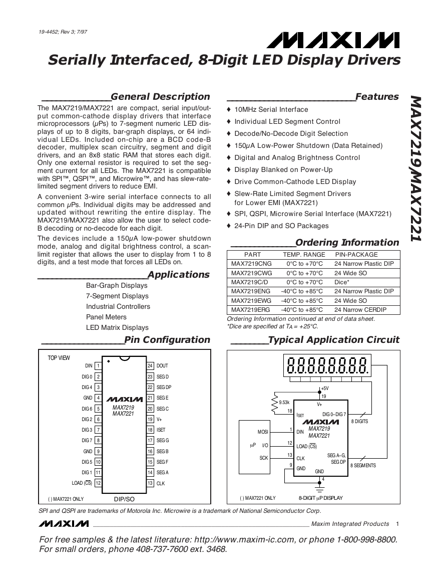
The MAX7219/MAX7221 are compact, serial input/out-
put common-cathode display drivers that interface
microprocessors (µPs) to 7-segment numeric LED dis-
plays of up to 8 digits, bar-graph displays, or 64 indi-
vidual LEDs. Included on-chip are a BCD code-B
decoder, multiplex scan circuitry, segment and digit
drivers, and an 8x8 static RAM that stores each digit.
Only one external resistor is required to set the seg-
ment current for all LEDs. The MAX7221 is compatible
with SPI™, QSPI™, and Microwire™, and has slew-rate-
limited segment drivers to reduce EMI.
A convenient 3-wire serial interface connects to all
common µPs. Individual digits may be addressed and
updated without rewriting the entire display. The
MAX7219/MAX7221 also allow the user to select code-
B decoding or no-decode for each digit.
The devices include a 150µA low-power shutdown
mode, analog and digital brightness control, a scan-
limit register that allows the user to display from 1 to 8
digits, and a test mode that forces all LEDs on.
________________________Applications
Bar-Graph Displays
7-Segment Displays
Industrial Controllers
Panel Meters
LED Matrix Displays
__________________Pin Configuration
TOP VIEW
M
A
X
7
2
1
9
/
M
A
X
7
2
2
1
____________________________Features
' 10MHz Serial Interface
' Individual LED Segment Control
' Decode/No-Decode Digit Selection
' 150µA Low-Power Shutdown (Data Retained)
' Digital and Analog Brightness Control
' Display Blanked on Power-Up
' Drive Common-Cathode LED Display
' Slew-Rate Limited Segment Drivers
for Lower EMI (MAX7221)
' SPI, QSPI, Microwire Serial Interface (MAX7221)
' 24-Pin DIP and SO Packages
______________Ordering Information
PART
MAX7219CNG
MAX7219CWG
MAX7219C/D
MAX7219ENG
MAX7219EWG
MAX7219ERG
TEMP. RANGE
0°C to +70°C
0°C to +70°C
0°C to +70°C
-40°C to +85°C
-40°C to +85°C
-40°C to +85°C
PIN-PACKAGE
24 Narrow Plastic DIP
24 Wide SO
Dice*
24 Narrow Plastic DIP
24 Wide SO
24 Narrow CERDIP
Ordering Information continued at end of data sheet.
*Dice are specified at TA = +25°C.
________Typical Application Circuit
MAX7219
MAX7221
DIN
DIG 0
DIG 4
GND
DIG 6
DIG 2
DIG 3
DIG 7
GND
DIG 5
DIG 1
LOAD (CS)
1
2
3
4
5
6
7
8
9
10
11
12
24
23
22
21
20
19
18
17
16
15
14
13
DOUT
SEG D
SEG DP
SEG E
SEG C
V+
ISET
SEG G
SEG B
SEG F
SEG A
CLK
9.53k
18
1
12
13
9
+5V
19
V+
DIG 0–DIG 7
MAX7219
MAX7221
ISET
DIN
8 DIGITS
LOAD (CS)
CLK
GND
GND
4
SEG A–G,
SEG DP
8 SEGMENTS
m P
MOSI
I/O
SCK
( ) MAX7221 ONLY
DIP/SO
( ) MAX7221 ONLY
8-DIGIT m P DISPLAY
SPI and QSPI are trademarks of Motorola Inc. Microwire is a trademark of National Semiconductor Corp.
________________________________________________________________ Maxim Integrated Products 1
For free samples & the latest literature: http://www.maxim-ic.com, or phone 1-800-998-8800.
For small orders, phone 408-737-7600 ext. 3468.
�
Serially Interfaced, 8-Digit LED Display Drivers
1
2
2
7
X
A
M
/
9
1
2
7
X
A
M
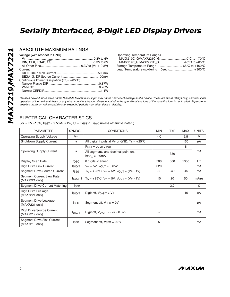
ABSOLUTE MAXIMUM RATINGS
Voltage (with respect to GND)
V+ ............................................................................-0.3V to 6V
DIN, CLK, LOAD, CS ...............................................-0.3V to 6V
All Other Pins.............................................-0.3V to (V+ + 0.3V)
Current
DIG0–DIG7 Sink Current................................................500mA
SEGA–G, DP Source Current.........................................100mA
Continuous Power Dissipation (TA = +85°C)
Narrow Plastic DIP ..........................................................0.87W
Wide SO ..........................................................................0.76W
Narrow CERDIP.................................................................1.1W
Operating Temperature Ranges
MAX7219C_G/MAX7221C_G ..............................0°C to +70°C
MAX7219E_G/MAX7221E_G ............................-40°C to +85°C
Storage Temperature Range .............................-65°C to +160°C
Lead Temperature (soldering, 10sec) .............................+300°C
Stresses beyond those listed under “Absolute Maximum Ratings” may cause permanent damage to the device. These are stress ratings only, and functional
operation of the device at these or any other conditions beyond those indicated in the operational sections of the specifications is not implied. Exposure to
absolute maximum rating conditions for extended periods may affect device reliability.
ELECTRICAL CHARACTERISTICS
(V+ = 5V ±10%, RSET = 9.53kΩ ±1%, TA = TMIN to TMAX, unless otherwise noted.)
PARAMETER
SYMBOL
CONDITIONS
Operating Supply Voltage
Shutdown Supply Current
Operating Supply Current
Display Scan Rate
Digit Drive Sink Current
Segment Drive Source Current
Segment Current Slew Rate
(MAX7221 only)
Segment Drive Current Matching
Digit Drive Leakage
(MAX7221 only)
Segment Drive Leakage
(MAX7221 only)
Digit Drive Source Current
(MAX7219 only)
Segment Drive Sink Current
(MAX7219 only)
V+
I+
I+
fOSC
IDIGIT
ISEG
∆ISEG/∆t
∆ISEG
All digital inputs at V+ or GND, TA = +25°C
RSET = open circuit
All segments and decimal point on,
ISEG_ = -40mA
8 digits scanned
V+ = 5V, VOUT = 0.65V
TA = +25°C, V+ = 5V, VOUT = (V+ - 1V)
TA = +25°C, V+ = 5V, VOUT = (V+ - 1V)
IDIGIT
Digit off, VDIGIT = V+
ISEG
Segment off, VSEG = 0V
IDIGIT
Digit off, VDIGIT = (V+ - 0.3V)
ISEG
Segment off, VSEG = 0.3V
MIN
4.0
500
320
-30
10
-2
5
TYP
MAX
UNITS
330
800
-40
20
3.0
5.5
150
8
1300
-45
50
-10
1
V
µA
mA
Hz
mA
mA
mA/µs
%
µA
µA
mA
mA
2
_______________________________________________________________________________________
�
Serially Interfaced, 8-Digit LED Display Drivers
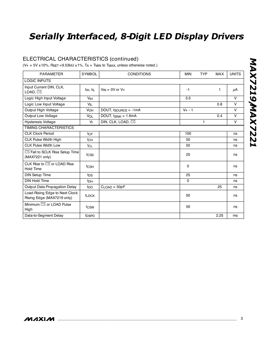
ELECTRICAL CHARACTERISTICS (continued)
(V+ = 5V ±10%, RSET =9.53kΩ ±1%, TA = TMIN to TMAX, unless otherwise noted.)
PARAMETER
SYMBOL
CONDITIONS
MIN
TYP
MAX
UNITS
LOGIC INPUTS
Input Current DIN, CLK,
LOAD, CS
Logic High Input Voltage
Logic Low Input Voltage
Output High Voltage
Output Low Voltage
Hysteresis Voltage
TIMING CHARACTERISTICS
CLK Clock Period
CLK Pulse Width High
CLK Pulse Width Low
CS Fall to SCLK Rise Setup Time
(MAX7221 only)
CLK Rise to CS or LOAD Rise
Hold Time
DIN Setup Time
DIN Hold Time
Output Data Propagation Delay
Load-Rising Edge to Next Clock
Rising Edge (MAX7219 only)
Minimum CS or LOAD Pulse
High
Data-to-Segment Delay
IIH, IIL
VIN = 0V or V+
DOUT, ISOURCE = -1mA
DOUT, ISINK = 1.6mA
DIN, CLK, LOAD, CS
CLOAD = 50pF
VIH
VIL
VOH
VOL
∆VI
tCP
tCH
tCL
tCSS
tCSH
tDS
tDH
tDO
tLDCK
tCSW
tDSPD
-1
3.5
V+ - 1
100
50
50
25
0
25
0
50
50
1
µA
0.8
0.4
1
25
2.25
V
V
V
V
V
ns
ns
ns
ns
ns
ns
ns
ns
ns
ns
ms
M
A
X
7
2
1
9
/
M
A
X
7
2
2
1
_______________________________________________________________________________________ 3
�
1
2
2
7
X
A
M
/
9
1
2
7
X
A
M
Serially Interfaced, 8-Digit LED Display Drivers
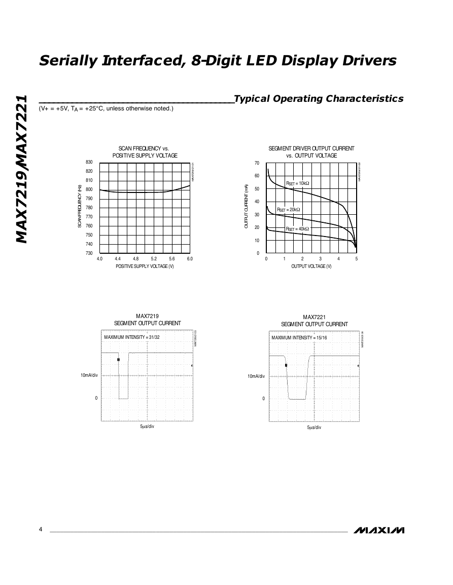
__________________________________________Typical Operating Characteristics
(V+ = +5V, TA = +25°C, unless otherwise noted.)
SCAN FREQUENCY vs.
POSITIVE SUPPLY VOLTAGE
SEGMENT DRIVER OUTPUT CURRENT
vs. OUTPUT VOLTAGE
1
0
1
2
/
9
1
2
7
X
A
M
6.0
3
0
1
2
/
9
1
2
7
X
A
M
2
0
1
2
/
9
1
2
7
X
A
M
RSET = 10kW
RSET = 20kW
RSET = 40kW
0
1
2
3
4
5
OUTPUT VOLTAGE (V)
MAX7221
SEGMENT OUTPUT CURRENT
MAXIMUM INTENSITY = 15/16
4
0
1
2
/
9
1
2
7
X
A
M
)
A
m
(
T
N
E
R
R
U
C
T
U
P
T
U
O
70
60
50
40
30
20
10
0
10mA/div
0
4.8
4.4
5.6
POSITIVE SUPPLY VOLTAGE (V)
5.2
MAX7219
SEGMENT OUTPUT CURRENT
MAXIMUM INTENSITY = 31/32
)
z
H
(
Y
C
N
E
U
Q
E
R
F
N
A
C
S
830
820
810
800
790
780
770
760
750
740
730
4.0
10mA/div
0
5m s/div
5m s/div
4
_______________________________________________________________________________________
�
Serially Interfaced, 8-Digit LED Display Drivers
______________________________________________________________Pin Description
PIN
1
2, 3, 5–8,
10, 11
4, 9
12
13
14–17,
20–23
18
19
24
NAME
DIN
DIG 0–DIG 7
GND
LOAD
(MAX7219)
CS
(MAX7221)
CLK
SEG A–SEG G,
DP
ISET
V+
DOUT
FUNCTION
Serial-Data Input. Data is loaded into the internal 16-bit shift register on CLK’s rising edge.
Eight-Digit Drive Lines that sink current from the display common cathode. The MAX7219 pulls
the digit outputs to V+ when turned off. The MAX7221’s digit drivers are high-impedance when
turned off.
Ground (both GND pins must be connected)
Load-Data Input. The last 16 bits of serial data are latched on LOAD’s rising edge.
Chip-Select Input. Serial data is loaded into the shift register while CS is low. The last 16 bits of
serial data are latched on CS’s rising edge.
Serial-Clock Input. 10MHz maximum rate. On CLK’s rising edge, data is shifted into the inter-
nal shift register. On CLK’s falling edge, data is clocked out of DOUT. On the MAX7221, the
CLK input is active only while CS is low.
Seven Segment Drives and Decimal Point Drive that source current to the display. On the
MAX7219, when a segment driver is turned off it is pulled to GND. The MAX7221 segment dri-
vers are high-impedance when turned off.
Connect to VDD through a resistor (RSET) to set the peak segment current (Refer to Selecting
RSETResistor section).
Positive Supply Voltage. Connect to +5V.
Serial-Data Output. The data into DIN is valid at DOUT 16.5 clock cycles later. This pin is used
to daisy-chain several MAX7219/MAX7221’s and is never high-impedance.
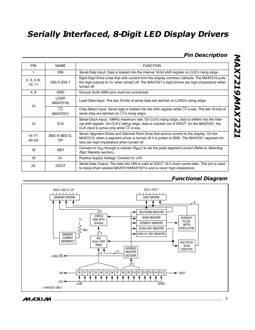
_________________________________________________________Functional Diagram
M
A
X
7
2
1
9
/
M
A
X
7
2
2
1
SEG A–SEG G, DP
SEGMENT DRIVERS
SEGMENT
CURRENT
REFERENCE
LOAD (CS)
DIN
CLK
( ) MAX7221 ONLY
DIG 0–DIG 7
DIGIT DRIVERS
SHUTDOWN REGISTER
MODE REGISTER
INTENSITY REGISTER
SCAN-LIMIT REGISTER
DISPLAY-TEST REGISTER
8
INTENSITY
PULSE-
WIDTH
MODULATOR
V+
RSET
8
CODE B
ROM WITH
BYPASS
8
8x8
DUAL-PORT
SRAM
8
8
ADDRESS
REGISTER
DECODER
4
MULTIPLEX
SCAN
CIRCUITRY
D0
D1 D2 D3 D4 D5 D6 D7 D8 D9 D10 D11 D12
D13 D14 D15
DOUT
(LSB)
(MSB)
_______________________________________________________________________________________ 5
�
Serially Interfaced, 8-Digit LED Display Drivers
1
2
2
7
X
A
M
/
9
1
2
7
X
A
M
CS
OR LOAD
CLK
DIN
DOUT
tCSS
tCL
tCH
tCSH
tCP
tCSW
tLDCK
tDH
tDS
D15
D14
D1
D0
tDO
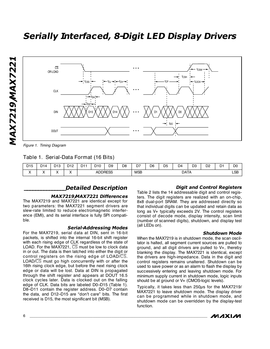
Figure 1. Timing Diagram
Table 1. Serial-Data Format (16 Bits)
D15
D14
D13
D12
D11
X
X
X
X
D9
D10
ADDRESS
D8
D7
MSB
D6
D5
D3
D4
MSB
DATA
D2
D1
D0
LSB
_______________Detailed Description
MAX7219/MAX7221 Differences
The MAX7219 and MAX7221 are identical except for
two parameters: the MAX7221 segment drivers are
slew-rate limited to reduce electromagnetic interfer-
ence (EMI), and its serial interface is fully SPI compati-
ble.
Serial-Addressing Modes
For the MAX7219, serial data at DIN, sent in 16-bit
packets, is shifted into the internal 16-bit shift register
with each rising edge of CLK regardless of the state of
LOAD. For the MAX7221, CS must be low to clock data
in or out. The data is then latched into either the digit or
control registers on the rising edge of LOAD/CS.
LOAD/CS must go high concurrently with or after the
16th rising clock edge, but before the next rising clock
edge or data will be lost. Data at DIN is propagated
through the shift register and appears at DOUT 16.5
clock cycles later. Data is clocked out on the falling
edge of CLK. Data bits are labeled D0–D15 (Table 1).
D8–D11 contain the register address. D0–D7 contain
the data, and D12–D15 are “don’t care” bits. The first
received is D15, the most significant bit (MSB).
Digit and Control Registers
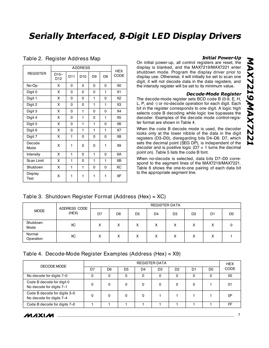
Table 2 lists the 14 addressable digit and control regis-
ters. The digit registers are realized with an on-chip,
8x8 dual-port SRAM. They are addressed directly so
that individual digits can be updated and retain data as
long as V+ typically exceeds 2V. The control registers
consist of decode mode, display intensity, scan limit
(number of scanned digits), shutdown, and display test
(all LEDs on).
Shutdown Mode
When the MAX7219 is in shutdown mode, the scan oscil-
lator is halted, all segment current sources are pulled to
ground, and all digit drivers are pulled to V+, thereby
blanking the display. The MAX7221 is identical, except
the drivers are high-impedance. Data in the digit and
control registers remains unaltered. Shutdown can be
used to save power or as an alarm to flash the display by
successively entering and leaving shutdown mode. For
minimum supply current in shutdown mode, logic inputs
should be at ground or V+ (CMOS-logic levels).
Typically, it takes less than 250µs for the MAX7219/
MAX7221 to leave shutdown mode. The display driver
can be programmed while in shutdown mode, and
shutdown mode can be overridden by the display-test
function.
6
_______________________________________________________________________________________
�
Serially Interfaced, 8-Digit LED Display Drivers
Table 2. Register Address Map
ADDRESS
REGISTER
D15–
D12
D11 D10
D9
D8
HEX
CODE
No-Op
Digit 0
Digit 1
Digit 2
Digit 3
Digit 4
Digit 5
Digit 6
Digit 7
Decode
Mode
Intensity
Scan Limit
Shutdown
Display
Test
X
X
X
X
X
X
X
X
X
X
X
X
X
X
0
0
0
0
0
0
0
0
1
1
1
1
1
1
0
0
0
0
1
1
1
1
0
0
0
0
1
1
0
0
1
1
0
0
1
1
0
0
1
1
0
1
0
1
0
1
0
1
0
1
0
1
0
1
0
1
X0
X1
X2
X3
X4
X5
X6
X7
X8
X9
XA
XB
XC
XF
Initial Power-Up
On initial power-up, all control registers are reset, the
display is blanked, and the MAX7219/MAX7221 enter
shutdown mode. Program the display driver prior to
display use. Otherwise, it will initially be set to scan one
digit, it will not decode data in the data registers, and
the intensity register will be set to its minimum value.
Decode-Mode Register
The decode-mode register sets BCD code B (0-9, E, H,
L, P, and -) or no-decode operation for each digit. Each
bit in the register corresponds to one digit. A logic high
selects code B decoding while logic low bypasses the
decoder. Examples of the decode mode control-regis-
ter format are shown in Table 4.
When the code B decode mode is used, the decoder
looks only at the lower nibble of the data in the digit
registers (D3–D0), disregarding bits D4–D6. D7, which
sets the decimal point (SEG DP), is independent of the
decoder and is positive logic (D7 = 1 turns the decimal
point on). Table 5 lists the code B font.
When no-decode is selected, data bits D7–D0 corre-
spond to the segment lines of the MAX7219/MAX7221.
Table 6 shows the one-to-one pairing of each data bit
to the appropriate segment line.
M
A
X
7
2
1
9
/
M
A
X
7
2
2
1
Table 3. Shutdown Register Format (Address (Hex) = XC)
MODE
ADDRESS CODE
(HEX)
D7
D6
D5
D4
D3
D2
D1
D0
REGISTER DATA
Shutdown
Mode
Normal
Operation
XC
XC
X
X
X
X
X
X
X
X
X
X
Table 4. Decode-Mode Register Examples (Address (Hex) = X9)
DECODE MODE
No decode for digits 7–0
Code B decode for digit 0
No decode for digits 7–1
Code B decode for digits 3–0
No decode for digits 7–4
Code B decode for digits 7–0
REGISTER DATA
D7
0
0
0
1
D6
0
0
0
1
D5
0
0
0
1
D4
0
0
0
1
D3
0
0
1
1
D2
0
0
1
1
X
X
D1
0
0
1
1
X
X
D0
0
1
1
1
0
1
HEX
CODE
00
01
0F
FF
_______________________________________________________________________________________ 7
�
Serially Interfaced, 8-Digit LED Display Drivers
1
2
2
7
X
A
M
/
9
1
2
7
X
A
M
Table 5. Code B Font
7-SEGMENT
CHARACTER
REGISTER DATA
ON SEGMENTS = 1
D7*
D6–D4
D3
D2
D1
D0
DP*
A
B
C
D
0
1
2
3
4
5
6
7
8
9
—
E
H
L
P
blank
X
X
X
X
X
X
X
X
X
X
X
X
X
X
X
X
0
0
0
0
0
0
0
0
1
1
1
1
1
1
1
1
0
0
0
0
1
1
1
1
0
0
0
0
1
1
1
1
0
0
1
1
0
0
1
1
0
0
1
1
0
0
1
1
0
1
0
1
0
1
0
1
0
1
0
1
0
1
0
1
1
0
1
1
0
1
1
1
1
1
0
1
0
0
1
0
1
1
1
1
1
0
0
1
1
1
0
0
1
0
1
0
1
1
0
1
1
1
1
1
1
1
0
0
1
0
0
0
1
0
1
1
0
1
1
0
1
1
0
1
0
1
0
0
E
1
0
1
0
0
0
1
0
1
0
0
1
1
1
1
0
F
1
0
0
0
1
1
1
0
1
1
0
1
1
1
1
0
G
0
0
1
1
1
1
1
0
1
1
1
1
1
0
1
0
*The decimal point is set by bit D7 = 1
Table 6. No-Decode Mode Data Bits and
Corresponding Segment Lines
A
G
B
C
F
E
STANDARD 7-SEGMENT LED
D
DP
D7
D6
REGISTER DATA
D5
D2
D3
D4
D1
D0
Corresponding
Segment Line
DP
A
B
C
D
E
F
G
Intensity Control
and Interdigit Blanking
The MAX7219/MAX7221 allow display brightness to be
controlled with an external resistor (RSET) connected
between V+ and ISET. The peak current sourced from
the segment drivers is nominally 100 times the current
entering ISET. This resistor can either be fixed or vari-
able to allow brightness adjustment from the front
panel. Its minimum value should be 9.53Ω, which typi-
cally sets the segment current at 40mA. Display bright-
ness can also be controlled digitally by using the
intensity register.
Digital control of display brightness is provided by an
internal pulse-width modulator, which is controlled by
the lower nibble of the intensity register. The modulator
scales the average segment current in 16 steps from a
maximum of 31/32 down to 1/32 of the peak current set
by RSET (15/16 to 1/16 on MAX7221). Table 7 lists the
intensity register format. The minimum interdigit blank-
ing time is set to 1/32 of a cycle.
8
_______________________________________________________________________________________
�


 2023年江西萍乡中考道德与法治真题及答案.doc
 2012年重庆南川中考生物真题及答案.doc
 2013年江西师范大学地理学综合及文艺理论基础考研真题.doc
 2020年四川甘孜小升初语文真题及答案I卷.doc
 2020年注册岩土工程师专业基础考试真题及答案.doc
 2023-2024学年福建省厦门市九年级上学期数学月考试题及答案.doc
 2021-2022学年辽宁省沈阳市大东区九年级上学期语文期末试题及答案.doc
 2022-2023学年北京东城区初三第一学期物理期末试卷及答案.doc
 2018上半年江西教师资格初中地理学科知识与教学能力真题及答案.doc
 2012年河北国家公务员申论考试真题及答案-省级.doc
 2020-2021学年江苏省扬州市江都区邵樊片九年级上学期数学第一次质量检测试题及答案.doc
 2022下半年黑龙江教师资格证中学综合素质真题及答案.doc