®
Introduction
White Paper
SDR SDRAM Controller
The single data rate (SDR) synchronous dynamic random access memory (SDRAM) controller provides a simplified
interface to industry standard SDR SDRAM. The SDR SDRAM Controller is available in either Verilog HDL or
VHDL and is optimized for the Altera® APEX™ architecture. The SDR SDRAM Controller supports the following
features:
■
■
■
■
■
■
■
■
■
Burst lengths of 1, 2, 4, or 8 data words
CAS latency of 2 or 3 clock cycles
16-bit programmable refresh counter used for automatic refresh
2-chip selects for SDRAM devices
Supports the NOP, READA, WRITEA, AUTO_REFRESH, PRECHARGE, ACTIVATE, BURST_STOP,
and LOAD_MR commands
Support for full-page mode operation
Data mask line for write operations
PLL to increase system performance
Support for data-path widths of 16, 32, and 64 bits
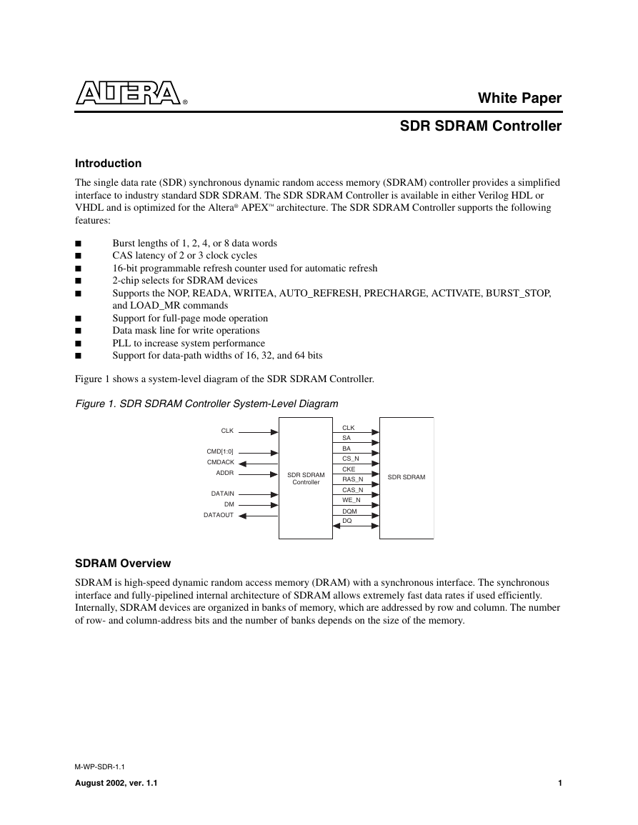
Figure 1 shows a system-level diagram of the SDR SDRAM Controller.
Figure 1. SDR SDRAM Controller System-Level Diagram
CLK
CMD[1:0]
CMDACK
ADDR
DATAIN
DM
DATAOUT
SDR SDRAM
Controller
CLK
SA
BA
CS_N
CKE
RAS_N
CAS_N
WE_N
DQM
DQ
SDR SDRAM
SDRAM Overview
SDRAM is high-speed dynamic random access memory (DRAM) with a synchronous interface. The synchronous
interface and fully-pipelined internal architecture of SDRAM allows extremely fast data rates if used efficiently.
Internally, SDRAM devices are organized in banks of memory, which are addressed by row and column. The number
of row- and column-address bits and the number of banks depends on the size of the memory.
M-WP-SDR-1.1
August 2002, ver. 1.1
1
�
Altera Corporation
SDR SDRAM Controller White Paper
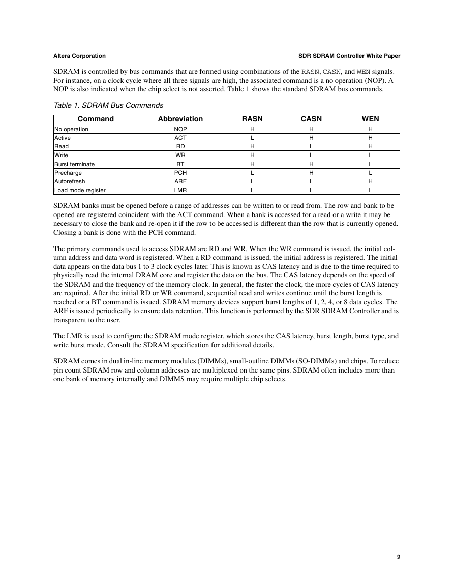
SDRAM is controlled by bus commands that are formed using combinations of the RASN, CASN, and WEN signals.
For instance, on a clock cycle where all three signals are high, the associated command is a no operation (NOP). A
NOP is also indicated when the chip select is not asserted. Table 1 shows the standard SDRAM bus commands.
Table 1. SDRAM Bus Commands
Command
Abbreviation
RASN
CASN
WEN
No operation
Active
Read
Write
Burst terminate
Precharge
Autorefresh
Load mode register
NOP
ACT
RD
WR
BT
PCH
ARF
LMR
H
L
H
H
H
L
L
L
H
H
L
L
H
H
L
L
H
H
H
L
L
L
H
L
SDRAM banks must be opened before a range of addresses can be written to or read from. The row and bank to be
opened are registered coincident with the ACT command. When a bank is accessed for a read or a write it may be
necessary to close the bank and re-open it if the row to be accessed is different than the row that is currently opened.
Closing a bank is done with the PCH command.
The primary commands used to access SDRAM are RD and WR. When the WR command is issued, the initial col-
umn address and data word is registered. When a RD command is issued, the initial address is registered. The initial
data appears on the data bus 1 to 3 clock cycles later. This is known as CAS latency and is due to the time required to
physically read the internal DRAM core and register the data on the bus. The CAS latency depends on the speed of
the SDRAM and the frequency of the memory clock. In general, the faster the clock, the more cycles of CAS latency
are required. After the initial RD or WR command, sequential read and writes continue until the burst length is
reached or a BT command is issued. SDRAM memory devices support burst lengths of 1, 2, 4, or 8 data cycles. The
ARF is issued periodically to ensure data retention. This function is performed by the SDR SDRAM Controller and is
transparent to the user.
The LMR is used to configure the SDRAM mode register. which stores the CAS latency, burst length, burst type, and
write burst mode. Consult the SDRAM specification for additional details.
SDRAM comes in dual in-line memory modules (DIMMs), small-outline DIMMs (SO-DIMMs) and chips. To reduce
pin count SDRAM row and column addresses are multiplexed on the same pins. SDRAM often includes more than
one bank of memory internally and DIMMS may require multiple chip selects.
2
�
Altera Corporation
Functional Description
SDR SDRAM Controller White Paper
Table 2 shows the SDR SDRAM Controller interface signals. All signals are synchronous to the system clock and
outputs are registered at the SDR SDRAM Controller’s outputs.
Table 2. Interface Signals
Signal
CLK
RESET_N
ADDR[ASIZE-1:0]
Name
Clock
Reset
Memory address
Active
NA
Low
NA
I/O
Input
Input
Input
Command
Command acknowledge High
NA
CMD[2:0]
CMDACK
DATAIN[DSIZE-1:0] Input data
DATAOUT[DSIZE-1:0] Output data
DM[(DSIZE/8)-1:0] Data mask
SA[11:0]
Address bus
NA
NA
High
NA
Description
System clock.
System reset.
Memory address for read/write requests. Width is set by
ASIZE.
Command request.
Input data bus. Width is set by DSIZE.
Input
Output Acknowledgment of the requested command.
Input
Output Output data bus. Width is set by DSIZE.
Input
Masks individual bytes during data write
Output SA[11:0] are sampled during the ACT command to latch
the row address. SA[n:0] are sampled during the RD/WR
command to latch the column address where n depends on
the size of SDRAM used. SA[10] is sampled during the
PCH command to determine if all banks are to be pre-
charged or the bank selected by BA[1:0]. The address out-
puts also provide the op-code during the LMR command.
BA[1:0]
Bank address
NA
Output These signals determine to which bank the ACT, RD, WR, or
PCH command is applied.
CS_N[1:0]
CKE
RAS_N
CAS_N
WE_N
DQ[DSIZE-1:0]
DQM[(DSIZE/8)-1:0] Data mask
Chip selects
Low
Clock enable
High
Row address strobe
Low
Column address strobe Low
Low
Write enable
NA
Data bus
High
Output SDRAM chip selects.
Output SDRAM CKE input.
Output SDRAM command input.
Output SDRAM command input.
Output SDRAM command input.
I/O
Output SDRAM data masks, mask individual bytes during data
SDRAM data bus.
write.
3
�
Altera Corporation
SDR SDRAM Controller White Paper
SDRAM Controller Command Interface
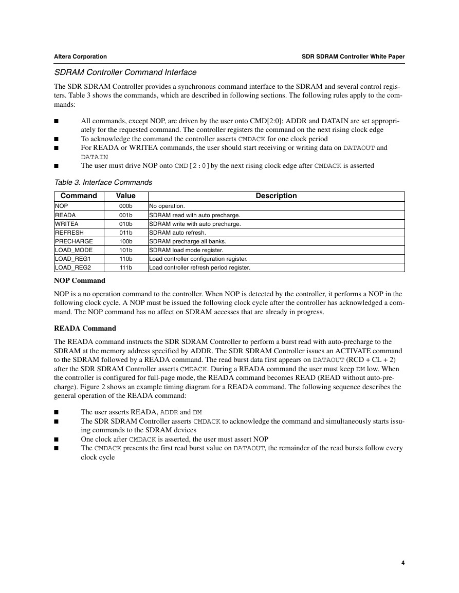
The SDR SDRAM Controller provides a synchronous command interface to the SDRAM and several control regis-
ters. Table 3 shows the commands, which are described in following sections. The following rules apply to the com-
mands:
■
■
■
■
All commands, except NOP, are driven by the user onto CMD[2:0]; ADDR and DATAIN are set appropri-
ately for the requested command. The controller registers the command on the next rising clock edge
To acknowledge the command the controller asserts CMDACK for one clock period
For READA or WRITEA commands, the user should start receiving or writing data on DATAOUT and
DATAIN
The user must drive NOP onto CMD[2:0]by the next rising clock edge after CMDACK is asserted
Description
Table 3. Interface Commands
Command
NOP
READA
WRITEA
REFRESH
PRECHARGE
LOAD_MODE
LOAD_REG1
LOAD_REG2
NOP Command
Value
000b
001b
010b
011b
100b
101b
110b
111b
No operation.
SDRAM read with auto precharge.
SDRAM write with auto precharge.
SDRAM auto refresh.
SDRAM precharge all banks.
SDRAM load mode register.
Load controller configuration register.
Load controller refresh period register.
NOP is a no operation command to the controller. When NOP is detected by the controller, it performs a NOP in the
following clock cycle. A NOP must be issued the following clock cycle after the controller has acknowledged a com-
mand. The NOP command has no affect on SDRAM accesses that are already in progress.
READA Command
The READA command instructs the SDR SDRAM Controller to perform a burst read with auto-precharge to the
SDRAM at the memory address specified by ADDR. The SDR SDRAM Controller issues an ACTIVATE command
to the SDRAM followed by a READA command. The read burst data first appears on DATAOUT (RCD + CL + 2)
after the SDR SDRAM Controller asserts CMDACK. During a READA command the user must keep DM low. When
the controller is configured for full-page mode, the READA command becomes READ (READ without auto-pre-
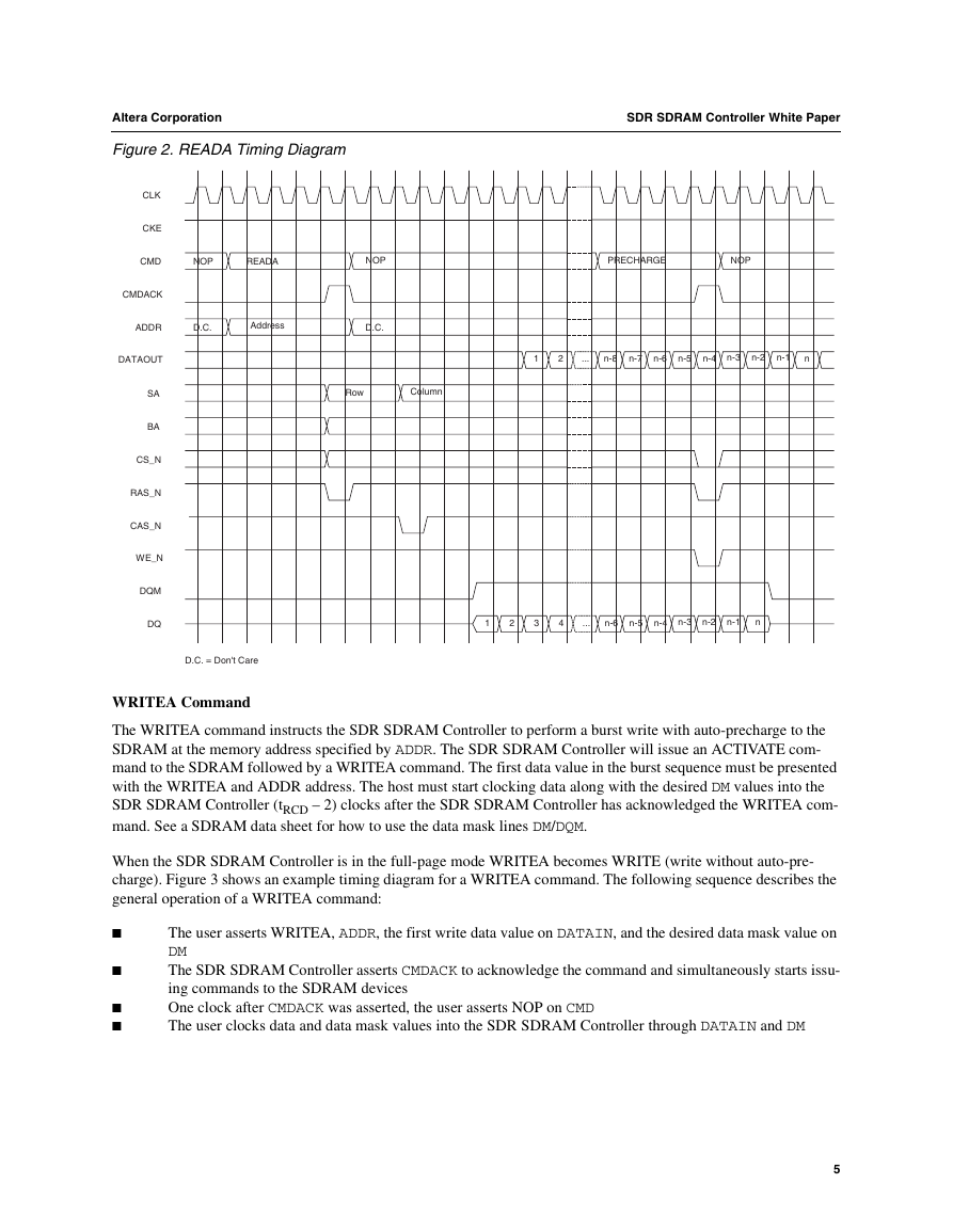
charge). Figure 2 shows an example timing diagram for a READA command. The following sequence describes the
general operation of the READA command:
■
■
■
■
The user asserts READA, ADDR and DM
The SDR SDRAM Controller asserts CMDACK to acknowledge the command and simultaneously starts issu-
ing commands to the SDRAM devices
One clock after CMDACK is asserted, the user must assert NOP
The CMDACK presents the first read burst value on DATAOUT, the remainder of the read bursts follow every
clock cycle
4
�
Altera Corporation
Figure 2. READA Timing Diagram
CLK
CKE
SDR SDRAM Controller White Paper
CMD
NOP
READA
NOP
PRECHARGE
NOP
CMDACK
ADDR
D.C.
Address
D.C.
1
2
...
n-8
n-7
n-6
n-5
n-4
n-3
n-2
n-1
n
Row
Column
1
2
3
4
...
n-6
n-5
n-4
n-3
n-2
n-1
n
DATAOUT
SA
BA
CS_N
RAS_N
CAS_N
WE_N
DQM
DQ
D.C. = Don't Care
WRITEA Command
The WRITEA command instructs the SDR SDRAM Controller to perform a burst write with auto-precharge to the
SDRAM at the memory address specified by ADDR. The SDR SDRAM Controller will issue an ACTIVATE com-
mand to the SDRAM followed by a WRITEA command. The first data value in the burst sequence must be presented
with the WRITEA and ADDR address. The host must start clocking data along with the desired DM values into the
SDR SDRAM Controller (tRCD – 2) clocks after the SDR SDRAM Controller has acknowledged the WRITEA com-
mand. See a SDRAM data sheet for how to use the data mask lines DM/DQM.
When the SDR SDRAM Controller is in the full-page mode WRITEA becomes WRITE (write without auto-pre-
charge). Figure 3 shows an example timing diagram for a WRITEA command. The following sequence describes the
general operation of a WRITEA command:
■
■
■
■
The user asserts WRITEA, ADDR, the first write data value on DATAIN, and the desired data mask value on
DM
The SDR SDRAM Controller asserts CMDACK to acknowledge the command and simultaneously starts issu-
ing commands to the SDRAM devices
One clock after CMDACK was asserted, the user asserts NOP on CMD
The user clocks data and data mask values into the SDR SDRAM Controller through DATAIN and DM
5
�
SDR SDRAM Controller White Paper
Altera Corporation
Figure 3. WRITEA Timing Diagram
CLK
CKE
CMD
NOP
WRITEA
NOP
CMDACK
ADDR
D.C.
Address
D.C.
DATAIN
D.C.
1
2
3
4
5
6
7
8
DM
D.C.
D.C.
D.C.
Row
Column
1
2
3
4
5
6
7
8
SA
BA
CS_N
RAS_N
CAS_N
WE_N
DQM
DQ
D.C. = Don't Care
REFRESH Command
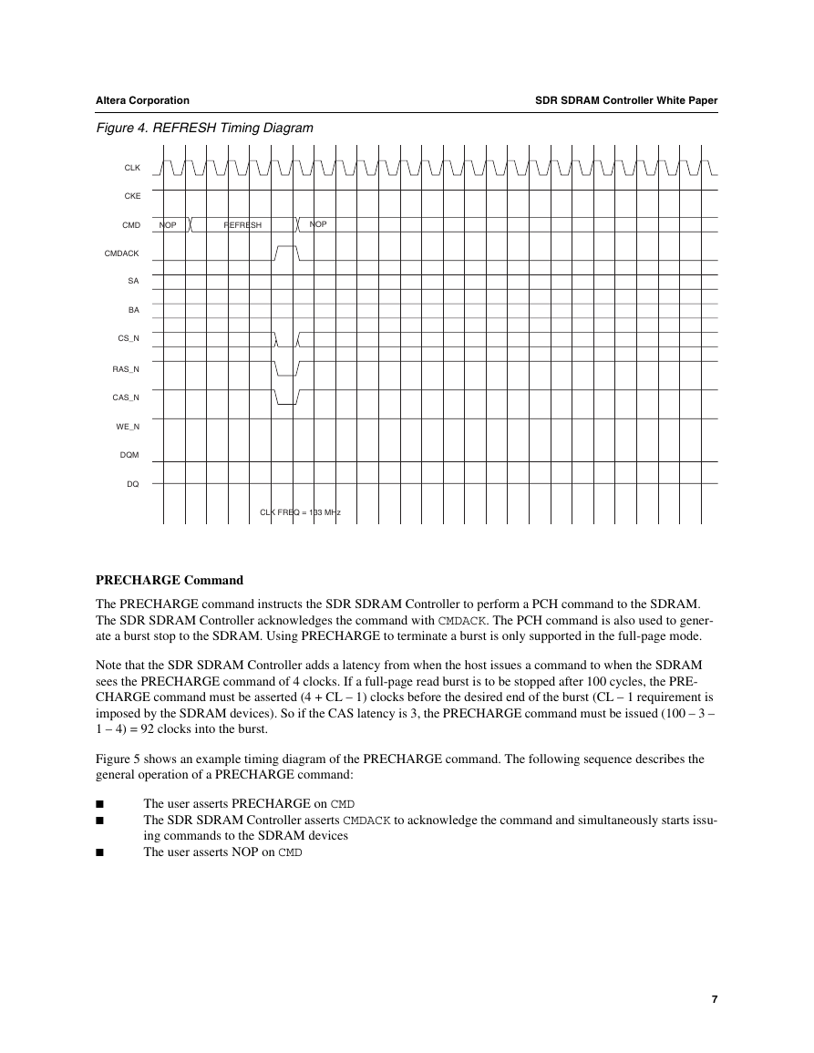
The REFRESH command instructs the SDR SDRAM Controller to perform an ARF command to the SDRAM. The
SDR SDRAM Controller acknowledges the REFRESH command with CMDACK. Figure 4 shows an example timing
diagram of the REFRESH command. The following sequence describes the general operation of a REFRESH com-
mand:
■
■
■
The user asserts REFRESH on the CMD input
The SDR SDRAM Controller asserts CMDACK to acknowledge the command and simultaneously starts issu-
ing commands to the SDRAM devices
The user asserts NOP on CMD
6
�
Altera Corporation
SDR SDRAM Controller White Paper
Figure 4. REFRESH Timing Diagram
CLK
CKE
CMD
NOP
REFRESH
NOP
CMDACK
SA
BA
CS_N
RAS_N
CAS_N
WE_N
DQM
DQ
CLK FREQ = 133 MHz
PRECHARGE Command
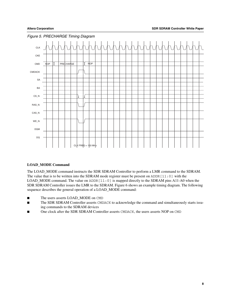
The PRECHARGE command instructs the SDR SDRAM Controller to perform a PCH command to the SDRAM.
The SDR SDRAM Controller acknowledges the command with CMDACK. The PCH command is also used to gener-
ate a burst stop to the SDRAM. Using PRECHARGE to terminate a burst is only supported in the full-page mode.
Note that the SDR SDRAM Controller adds a latency from when the host issues a command to when the SDRAM
sees the PRECHARGE command of 4 clocks. If a full-page read burst is to be stopped after 100 cycles, the PRE-
CHARGE command must be asserted (4 + CL – 1) clocks before the desired end of the burst (CL – 1 requirement is
imposed by the SDRAM devices). So if the CAS latency is 3, the PRECHARGE command must be issued (100 – 3 –
1 – 4) = 92 clocks into the burst.
Figure 5 shows an example timing diagram of the PRECHARGE command. The following sequence describes the
general operation of a PRECHARGE command:
■
■
■
The user asserts PRECHARGE on CMD
The SDR SDRAM Controller asserts CMDACK to acknowledge the command and simultaneously starts issu-
ing commands to the SDRAM devices
The user asserts NOP on CMD
7
�
Altera Corporation
SDR SDRAM Controller White Paper
Figure 5. PRECHARGE Timing Diagram
CLK
CKE
CMD
NOP
PRECHARGE
NOP
CMDACK
SA
BA
CS_N
RAS_N
CAS_N
WE_N
DQM
DQ
CLK FREQ = 133 MHz
LOAD_MODE Command
The LOAD_MODE command instructs the SDR SDRAM Controller to perform a LMR command to the SDRAM.
The value that is to be written into the SDRAM mode register must be present on ADDR[11:0] with the
LOAD_MODE command. The value on ADDR[11:0] is mapped directly to the SDRAM pins A11-A0 when the
SDR SDRAM Controller issues the LMR to the SDRAM. Figure 6 shows an example timing diagram. The following
sequence describes the general operation of a LOAD_MODE command:
■
■
■
The users asserts LOAD_MODE on CMD
The SDR SDRAM Controller asserts CMDACK to acknowledge the command and simultaneously starts issu-
ing commands to the SDRAM devices
One clock after the SDR SDRAM Controller asserts CMDACK, the users asserts NOP on CMD
8
�




 2023年江西萍乡中考道德与法治真题及答案.doc
 2012年重庆南川中考生物真题及答案.doc
 2013年江西师范大学地理学综合及文艺理论基础考研真题.doc
 2020年四川甘孜小升初语文真题及答案I卷.doc
 2020年注册岩土工程师专业基础考试真题及答案.doc
 2023-2024学年福建省厦门市九年级上学期数学月考试题及答案.doc
 2021-2022学年辽宁省沈阳市大东区九年级上学期语文期末试题及答案.doc
 2022-2023学年北京东城区初三第一学期物理期末试卷及答案.doc
 2018上半年江西教师资格初中地理学科知识与教学能力真题及答案.doc
 2012年河北国家公务员申论考试真题及答案-省级.doc
 2020-2021学年江苏省扬州市江都区邵樊片九年级上学期数学第一次质量检测试题及答案.doc
 2022下半年黑龙江教师资格证中学综合素质真题及答案.doc