Low Power HDMI Transmitter
User Guide — EP952_UG V0.4
EP952
User Guide
V0.4
Revised: Nov. 24, 2011
Original Release Date: Sep. 27, 2010
Explore
Explore reserves the right to make changes without further notice to any products herein to improve reliability, function or design. Explore
does not assume any liability arising out of the application or use of any product or circuit described herein; neither does it convey any license
under its patent rights nor the rights of others. Explore products are not designed, intended, or authorized for use as components in systems
intended for surgical implant into the body, or other applications intended to support or sustain life, or for any other application in which
the failure of the Explore product could create a situation where personal injury or death may occur. Should Buyer purchase or use Explore
products for any such unintended or unauthorized application, Buyer shall indemnify and hold Explore and its officers, employees,
subsidiaries, affiliates, and distributors harmless against all claims, costs, damages, and expenses, and reasonable attorney fees arising out of,
directly or indirectly, any claim of personal injury or death associated with such unintended or unauthorized use, even if such claim alleges
that Explore was negligent regarding the design or manufacture of the part.
Explore Microelectronics Confidential Proprietary
NON-DISCLOSURE AGREEMENT REQUIRED
1
�
User Guide — EP952_UG V0.4
Revision History
Version
Number
Revision
Date
Author
Description of Changes
0.0
0.1
Sep/27/2010
Ether Lai
Initial Version
Dec/01/2010
Ether Lai
Add the Pin Diagram of BGA-64 package;
Add the detailed package outline dimension;
Update BGA-64 package outline dimension;
0.2
Apr/11/2011
Ether Lai
Add the Ordering Information for different type of chip configuration;
Revise Package Footprint Diagram;
Fix typo in Register Description;
Mar/03/2011
Ether Lai
Add the Thermal Resistance;
0.3
0.4
Sep/14/2011
Kyle Kuo
Add the Power Consumption
Revised EXT_SWING Resistor Value to 820 Ohm
Nov/24/2011
Kyle Kuo
Remove Device Part of K Serial
2
Explore Microelectronics Confidential Proprietary
NON-DISCLOSURE AGREEMENT REQUIRED
�
User Guide — EP952_UG V0.4
Section 1 Introduction
1.1 Overview
EP952 is a Low Power HDMI (High Definition Multimedia Interface) transmitter. The chip is compliant
with HDMI Rev 1.4 and HDCP Rev 1.4 specifications. The chip converts input video data in RGB or YUV
format and audio data in IIS or SPDIF format into HDMI differential signals. The chip supports 8-bit
video upto 1080p in HDMI mode. The chip also supports 3D video. The chip supports highly flexible
digital video input in a muxed 12-bits mode or non-muxed 24-bit mode input. In both modes, the chip
supports single or dual edge clocking.
1.2 Features
• HDMI Specification 1.4 Compliant
•
•
Integrated HDCP encryption engine which is compliant with HDCP Rev 1.4 specification for
transmitting protected content
Integrated on-chip HDCP Keys (Optional)
• Wide TMDS Clock Frequency Range: 25MHz - 165MHz in HDMI mode
•
•
•
•
•
•
•
•
•
Support 8-bit video upto 1080p in HDMI mode
Support 3D video
Support IIS and SPDIF (LPCM or compressed) audio types
Support auto-send for DVI, ADO, ACR (Audio Clock Regeneration) and General Control packets.
Support 1 Generic Data Packet buffer
Flexible digital video input: muxed 12-bit and non-muxed 24-bit mode in RGB or YUV, embedded
sync or separate sync
Support 1 port of SPDIF audio input (without the need for system clock) and 2 channels of IIS audio
inputs
Supports audio down sampling at 1/2, 1/3 or 1/4 sampling rate for both SPDIF and IIS
Supports CCIR YUV422 format input
• On-chip YUV422 to YUV444 conversion and YUV444 to YUV422 conversion
• On-chip YUV to RGB and RGB to YUB conversion in ITU-R BT.601 and 709 color space
• Register Programmable Single/Dual Edge Clocking Mode
•
IIC Slave Programming Interface
• Programmable DE generation
•
•
3
Supports x2, x4 and x8 Pixel Repetition
Supports input De-Skewing
Explore Microelectronics Confidential Proprietary
NON-DISCLOSURE AGREEMENT REQUIRED
�
User Guide — EP952_UG V0.4
•
Supports Receiver Hot Plug Detection
• Downward compatible with DVI 1.0
•
•
Supports Power Down Mode
3.3V and 1.8V power required
1.3 Ordering Information
Four parts with different Package Type and HDCP Key Configuration are provided:
Table 1-1 EP952 Ordering Information
Device Part #
Package Type
EP952
EP952B
LQFP-64 (7mm x 7mm)
BGA-64 (5mm x 5mm)
Pins
64
64
HDCP Keys
Write from External MCU
Write from External MCU
4
Explore Microelectronics Confidential Proprietary
NON-DISCLOSURE AGREEMENT REQUIRED
�
Section 2 Overview
2.1 Block Diagram
User Guide — EP952_UG V0.4
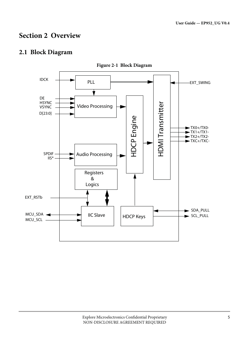
Figure 2-1 Block Diagram
PLL
EXT_SWING
r
e
t
t
i
m
s
n
a
r
T
I
M
D
H
TX0+/TX0-
TX1+/TX1-
TX2+/TX2-
TXC+/TXC-
i
e
n
g
n
E
P
C
D
H
IDCK
DE
HSYNC
VSYNC
D[23:0]
Video Processing
SPDIF
IIS*
Audio Processing
Registers
&
Logics
EXT_RSTb
MCU_SDA
MCU_SCL
IIC Slave
HDCP Keys
SDA_PULL
SCL_PULL
Explore Microelectronics Confidential Proprietary
NON-DISCLOSURE AGREEMENT REQUIRED
5
�
User Guide — EP952_UG V0.4
2.2 Pin Diagram
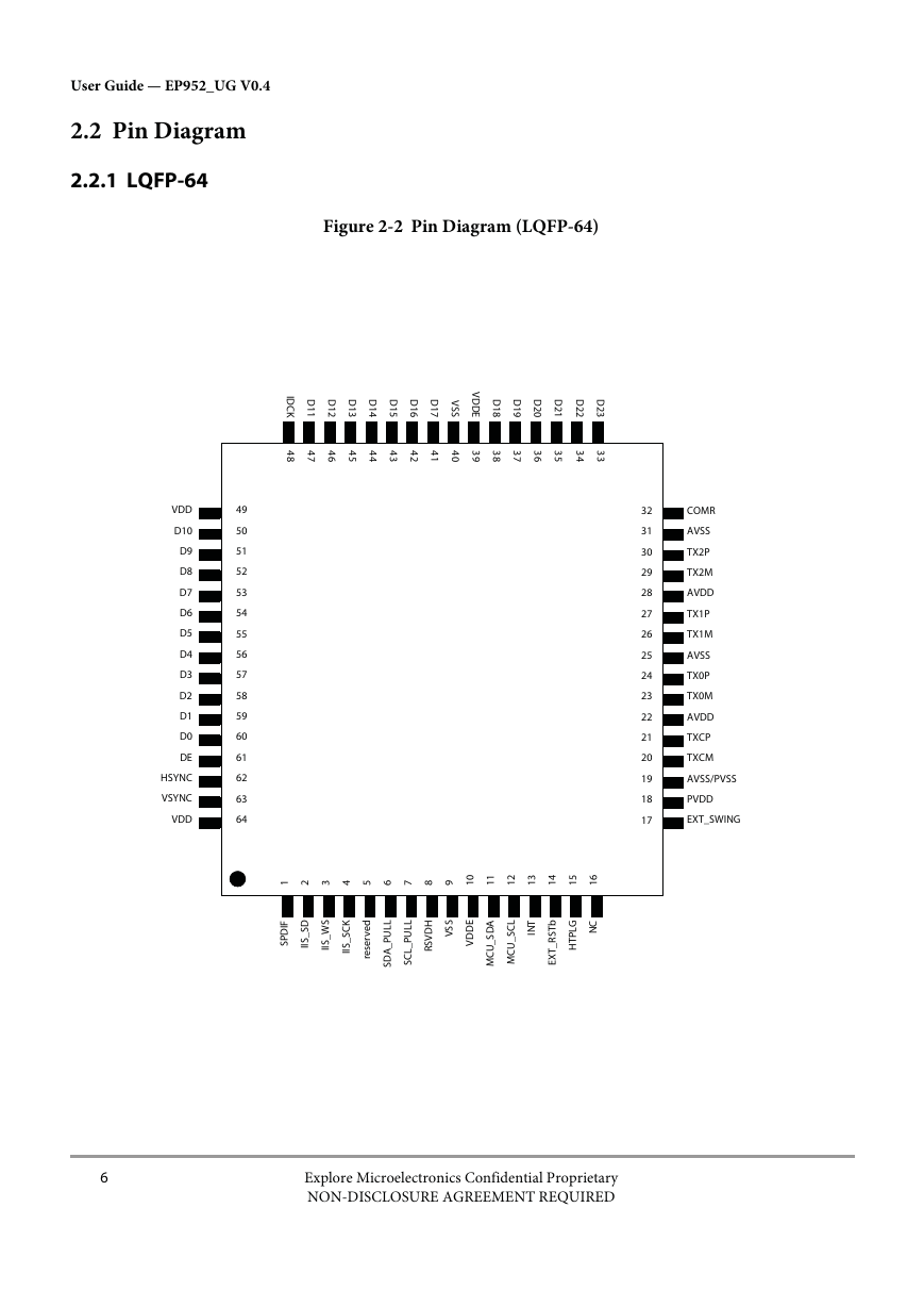
2.2.1 LQFP-64
VDD
D10
D9
D8
D7
D6
D5
D4
D3
D2
D1
D0
DE
HSYNC
VSYNC
VDD
49
50
51
52
53
54
55
56
57
58
59
60
61
62
63
64
Figure 2-2 Pin Diagram (LQFP-64)
I
D
C
K
D
1
1
D
1
2
D
1
3
D
1
4
D
1
5
D
1
6
D
1
7
V
S
S
V
D
D
E
D
1
8
D
1
9
D
2
0
D
2
1
D
2
2
D
2
3
4
8
4
7
4
6
4
5
4
4
4
3
4
2
4
1
4
0
3
9
3
8
3
7
3
6
3
5
3
4
3
3
32
31
30
29
28
27
26
25
24
23
22
21
20
19
18
17
COMR
AVSS
TX2P
TX2M
AVDD
TX1P
TX1M
AVSS
TX0P
TX0M
AVDD
TXCP
TXCM
AVSS/PVSS
PVDD
EXT_SWING
1
2
3
4
5
6
7
8
9
0
1
1
1
2
1
3
1
4
1
5
1
6
1
I
F
D
P
S
D
S
_
S
I
I
S
W
_
S
I
I
K
C
S
_
S
I
I
d
e
v
r
e
s
e
r
L
L
U
P
_
A
D
S
L
L
U
P
_
L
C
S
H
D
V
S
R
S
S
V
E
D
D
V
A
D
S
_
U
C
M
L
C
S
_
U
C
M
T
N
I
b
T
S
R
_
T
X
E
C
N
G
L
P
T
H
6
Explore Microelectronics Confidential Proprietary
NON-DISCLOSURE AGREEMENT REQUIRED
�
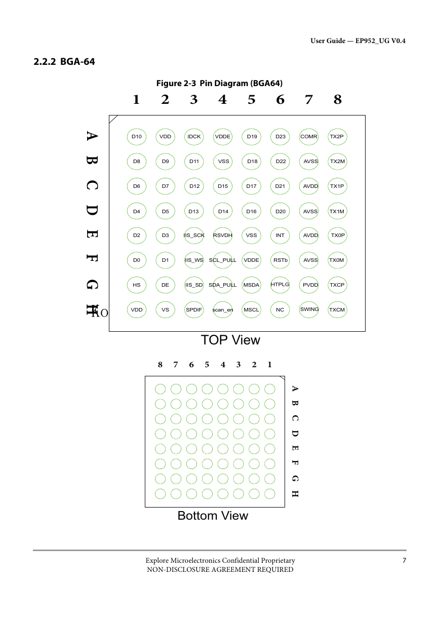
2.2.2 BGA-64
1
Figure 2-3 Pin Diagram (BGA64)
2
6
4
5
3
User Guide — EP952_UG V0.4
7
8
A
B
C
D
E
F
G
D10
VDD
IDCK
VDDE
D19
D23
COMR
TX2P
D8
D6
D4
D2
D0
D9
D7
D11
VSS
D18
D22
AVSS
TX2M
D12
D15
D17
D21
AVDD
TX1P
D5
D13
D14
D16
D20
AVSS
TX1M
D3
IIS_SCK
RSVDH
VSS
INT
AVDD
TX0P
D1
IIS_WS
SCL_PULL
VDDE
RSTb
AVSS
TX0M
HS
DE
IIS_SD
SDA_PULL
MSDA
HTPLG
PVDD
TXCP
H
scan_en
SWING
SPDIF
TXCM
MSCL
NC
VDD
VS
TOP View
8
7
6
5
4
3
2
1
A
B
C
D
E
F
G
H
Bottom View
Explore Microelectronics Confidential Proprietary
NON-DISCLOSURE AGREEMENT REQUIRED
7
�
User Guide — EP952_UG V0.4
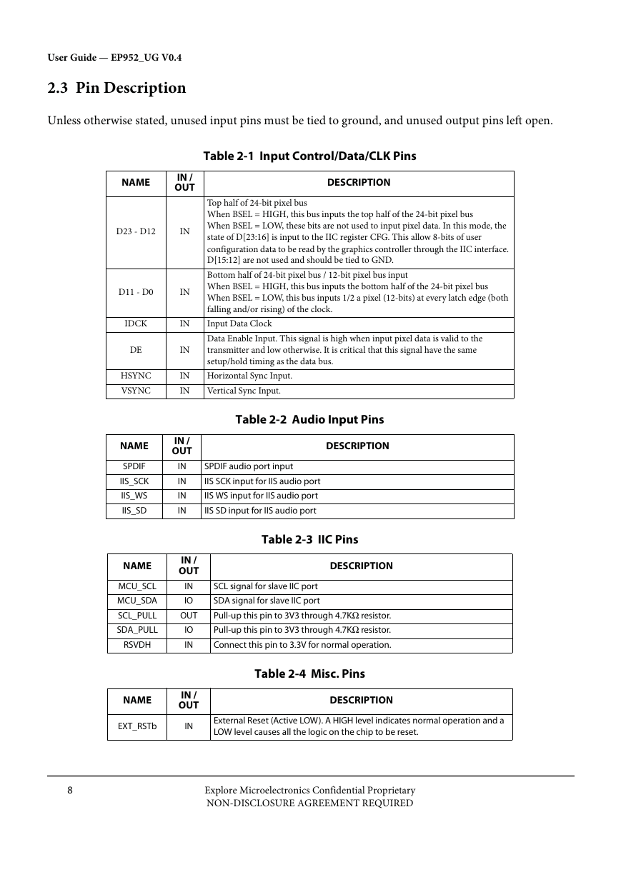
2.3 Pin Description
Unless otherwise stated, unused input pins must be tied to ground, and unused output pins left open.
NAME
IN /
OUT
D23 - D12
IN
D11 - D0
IN
Table 2-1 Input Control/Data/CLK Pins
DESCRIPTION
Top half of 24-bit pixel bus
When BSEL = HIGH, this bus inputs the top half of the 24-bit pixel bus
When BSEL = LOW, these bits are not used to input pixel data. In this mode, the
state of D[23:16] is input to the IIC register CFG. This allow 8-bits of user
configuration data to be read by the graphics controller through the IIC interface.
D[15:12] are not used and should be tied to GND.
Bottom half of 24-bit pixel bus / 12-bit pixel bus input
When BSEL = HIGH, this bus inputs the bottom half of the 24-bit pixel bus
When BSEL = LOW, this bus inputs 1/2 a pixel (12-bits) at every latch edge (both
falling and/or rising) of the clock.
IDCK
IN
Input Data Clock
DE
HSYNC
VSYNC
NAME
SPDIF
IIS_SCK
IIS_WS
IIS_SD
IN
IN
IN
IN /
OUT
IN
IN
IN
IN
NAME
MCU_SCL
MCU_SDA
IN /
OUT
IN
IO
SCL_PULL
OUT
SDA_PULL
RSVDH
IO
IN
NAME
IN /
OUT
EXT_RSTb
IN
Data Enable Input. This signal is high when input pixel data is valid to the
transmitter and low otherwise. It is critical that this signal have the same
setup/hold timing as the data bus.
Horizontal Sync Input.
Vertical Sync Input.
Table 2-2 Audio Input Pins
DESCRIPTION
SPDIF audio port input
IIS SCK input for IIS audio port
IIS WS input for IIS audio port
IIS SD input for IIS audio port
Table 2-3 IIC Pins
DESCRIPTION
SCL signal for slave IIC port
SDA signal for slave IIC port
Pull-up this pin to 3V3 through 4.7KΩ resistor.
Pull-up this pin to 3V3 through 4.7KΩ resistor.
Connect this pin to 3.3V for normal operation.
Table 2-4 Misc. Pins
DESCRIPTION
External Reset (Active LOW). A HIGH level indicates normal operation and a
LOW level causes all the logic on the chip to be reset.
8
Explore Microelectronics Confidential Proprietary
NON-DISCLOSURE AGREEMENT REQUIRED
�




 2023年江西萍乡中考道德与法治真题及答案.doc
 2012年重庆南川中考生物真题及答案.doc
 2013年江西师范大学地理学综合及文艺理论基础考研真题.doc
 2020年四川甘孜小升初语文真题及答案I卷.doc
 2020年注册岩土工程师专业基础考试真题及答案.doc
 2023-2024学年福建省厦门市九年级上学期数学月考试题及答案.doc
 2021-2022学年辽宁省沈阳市大东区九年级上学期语文期末试题及答案.doc
 2022-2023学年北京东城区初三第一学期物理期末试卷及答案.doc
 2018上半年江西教师资格初中地理学科知识与教学能力真题及答案.doc
 2012年河北国家公务员申论考试真题及答案-省级.doc
 2020-2021学年江苏省扬州市江都区邵樊片九年级上学期数学第一次质量检测试题及答案.doc
 2022下半年黑龙江教师资格证中学综合素质真题及答案.doc