DISCRETE SEMICONDUCTORS
DATA SHEET
book, halfpage
MBD128
BGA2771
MMIC wideband amplifier
Product specification
Supersedes data of 2001 Oct 19
2002 Aug 06
�
Philips Semiconductors
MMIC wideband amplifier
FEATURES
• Internally matched
• Wide frequency range
• Very flat gain
• High output power
• High linearity
• Unconditionally stable.
APPLICATIONS
• Cable systems
• LNB IF amplifiers
• General purpose
• ISM.
DESCRIPTION
Product specification
BGA2771
DESCRIPTION
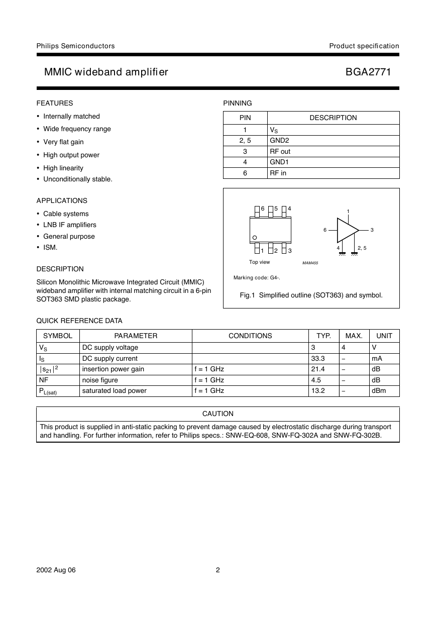
PINNING
PIN
1
2, 5
3
4
6
VS
GND2
RF out
GND1
RF in
6
5
4
1
6
3
1
2
3
4
2, 5
Top view
MAM455
Silicon Monolithic Microwave Integrated Circuit (MMIC)
wideband amplifier with internal matching circuit in a 6-pin
SOT363 SMD plastic package.
Marking code: G4-.
Fig.1 Simplified outline (SOT363) and symbol.
QUICK REFERENCE DATA
SYMBOL
VS
IS
s21 2
NF
PL(sat)
PARAMETER
CONDITIONS
TYP.
MAX.
UNIT
DC supply voltage
DC supply current
insertion power gain
noise figure
saturated load power
f = 1 GHz
f = 1 GHz
f = 1 GHz
CAUTION
4
3
33.3
21.4
4.5
13.2
V
mA
dB
dB
dBm
This product is supplied in anti-static packing to prevent damage caused by electrostatic discharge during transport
and handling. For further information, refer to Philips specs.: SNW-EQ-608, SNW-FQ-302A and SNW-FQ-302B.
2002 Aug 06
2
-
-
-
-
�
Philips Semiconductors
MMIC wideband amplifier
Product specification
BGA2771
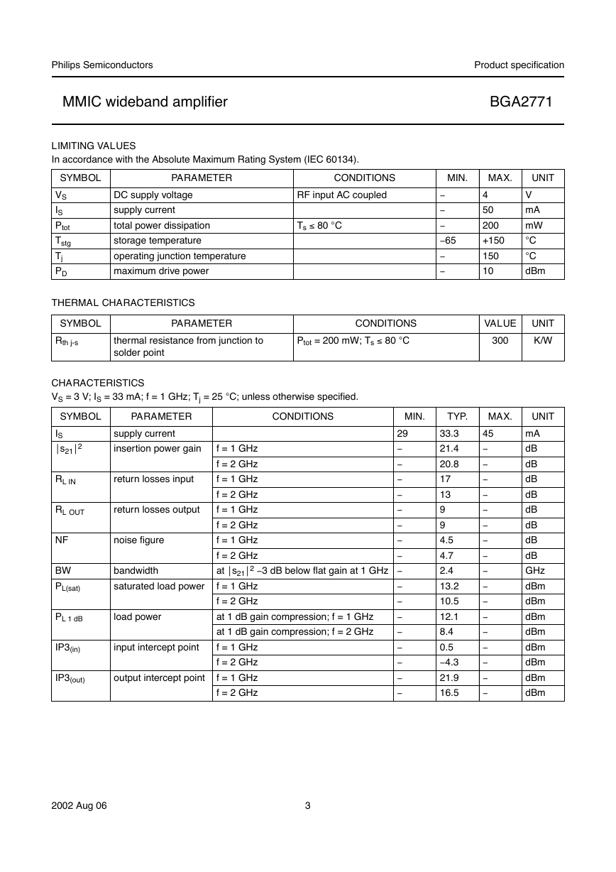
LIMITING VALUES
In accordance with the Absolute Maximum Rating System (IEC 60134).
SYMBOL
VS
IS
Ptot
Tstg
Tj
PD
PARAMETER
CONDITIONS
MIN.
MAX.
UNIT
DC supply voltage
supply current
total power dissipation
storage temperature
operating junction temperature
maximum drive power
RF input AC coupled
Ts £ 80 C
- 65
4
50
200
+150
150
10
V
mA
mW
C
C
dBm
THERMAL CHARACTERISTICS
SYMBOL
Rth j-s
PARAMETER
thermal resistance from junction to
solder point
CONDITIONS
Ptot = 200 mW; Ts £ 80 C
VALUE
300
UNIT
K/W
CHARACTERISTICS
VS = 3 V; IS = 33 mA; f = 1 GHz; Tj = 25 C; unless otherwise specified.
SYMBOL
IS
s21 2
PARAMETER
supply current
insertion power gain
RL IN
return losses input
RL OUT
return losses output
NF
noise figure
BW
PL(sat)
bandwidth
saturated load power
PL 1 dB
load power
IP3(in)
input intercept point
IP3(out)
output intercept point
CONDITIONS
MIN.
TYP.
29
f = 1 GHz
f = 2 GHz
f = 1 GHz
f = 2 GHz
f = 1 GHz
f = 2 GHz
f = 1 GHz
f = 2 GHz
at s21 2 - 3 dB below flat gain at 1 GHz -
f = 1 GHz
f = 2 GHz
at 1 dB gain compression; f = 1 GHz
at 1 dB gain compression; f = 2 GHz
f = 1 GHz
f = 2 GHz
f = 1 GHz
f = 2 GHz
33.3
21.4
20.8
17
13
9
9
4.5
4.7
2.4
13.2
10.5
12.1
8.4
0.5
- 4.3
21.9
16.5
MAX.
45
UNIT
mA
dB
dB
dB
dB
dB
dB
dB
dB
GHz
dBm
dBm
dBm
dBm
dBm
dBm
dBm
dBm
2002 Aug 06
3
-
-
-
-
-
-
-
-
-
-
-
-
-
-
-
-
-
-
-
-
-
-
-
-
-
-
-
-
-
-
-
-
-
-
-
-
-
-
�
Philips Semiconductors
MMIC wideband amplifier
APPLICATION INFORMATION
Figure 2 shows a typical application circuit for the
BGA2771 MMIC. The device is internally matched to 50 W
and therefore does not need any external matching. The
value of the input and output DC blocking capacitors C2
and C3 should be not more than 100 pF for applications
above 100 MHz. However, when the device is operated
below 100 MHz, the capacitor value should be increased.
,
The nominal value of the RF choke L1 is 100 nH. At
frequencies below 100 MHz this value should be
increased to 220 nH. At frequencies above 1 GHz a much
lower value must be used (e.g. 10 nH) to improve return
losses. For optimal results, a good quality chip inductor
such as the TDK MLG 1608 (0603), or a wire-wound SMD
type should be chosen.
Both the RF choke L1 and the 22 nF supply decoupling
capacitor C1 should be located as closely as possible to
the MMIC.
Separate paths must be used for the ground planes of the
ground pins GND1 and GND2, and these paths must be as
short as possible. When using vias, use multiple vias per
pin in order to limit ground path inductance.
handbook, halfpage
Vs
C1
C2
RF input
Vs
RF in
RF out
L1
C3
RF output
GND1
GND2
MGU436
Fig.2 Typical application circuit.
Figure 3 shows two cascaded MMICs. This configuration
doubles overall gain while preserving broadband
characteristics. Supply decoupling and grounding
conditions for each MMIC are the same as those for the
circuit of Fig.2.
The excellent wideband characteristics of the MMIC make
it and ideal building block in IF amplifier applications such
as LBNs (see Fig.4).
As a buffer amplifier between an LNA and a mixer in a
receiver circuit, the MMIC offers an easy matching, low
noise solution (see Fig.5).
2002 Aug 06
4
Product specification
BGA2771
In Fig.6 the MMIC is used as a driver to the power amplifier
as part of a transmitter circuit. Good linear performance
and matched input and output offer quick design solutions
in such applications.
handbook, halfpage
DC-block
100 pF
DC-block
100 pF
DC-block
100 pF
input
output
MGU437
Fig.3 Simple cascade circuit.
handbook, halfpage
from RF
circuit
mixer
to IF circuit
or demodulator
wideband
amplifier
MGU438
oscillator
Fig.4 IF amplifier application.
handbook, halfpage
antenna
mixer
to IF circuit
or demodulator
MGU439
LNA
wideband
amplifier
oscillator
Fig.5 RF amplifier application.
handbook, halfpage
from modulation
or IF circuit
mixer
oscillator
to power
amplifier
MGU440
wideband
amplifier
Fig.6 Power amplifier driver application.
�
Philips Semiconductors
MMIC wideband amplifier
Product specification
BGA2771
handbook, full pagewidth
90
+1
135
+0.5
45
+2
180
0
+0.2
- 0.2
0.2
0.5
3 GHz 100 MHz
2
1
5
1.0
0.8
0.6
0.4
0.2
0
+5
- 5
0
- 0.5
- 135
- 2
- 45
- 1
- 90
MGU457
1.0
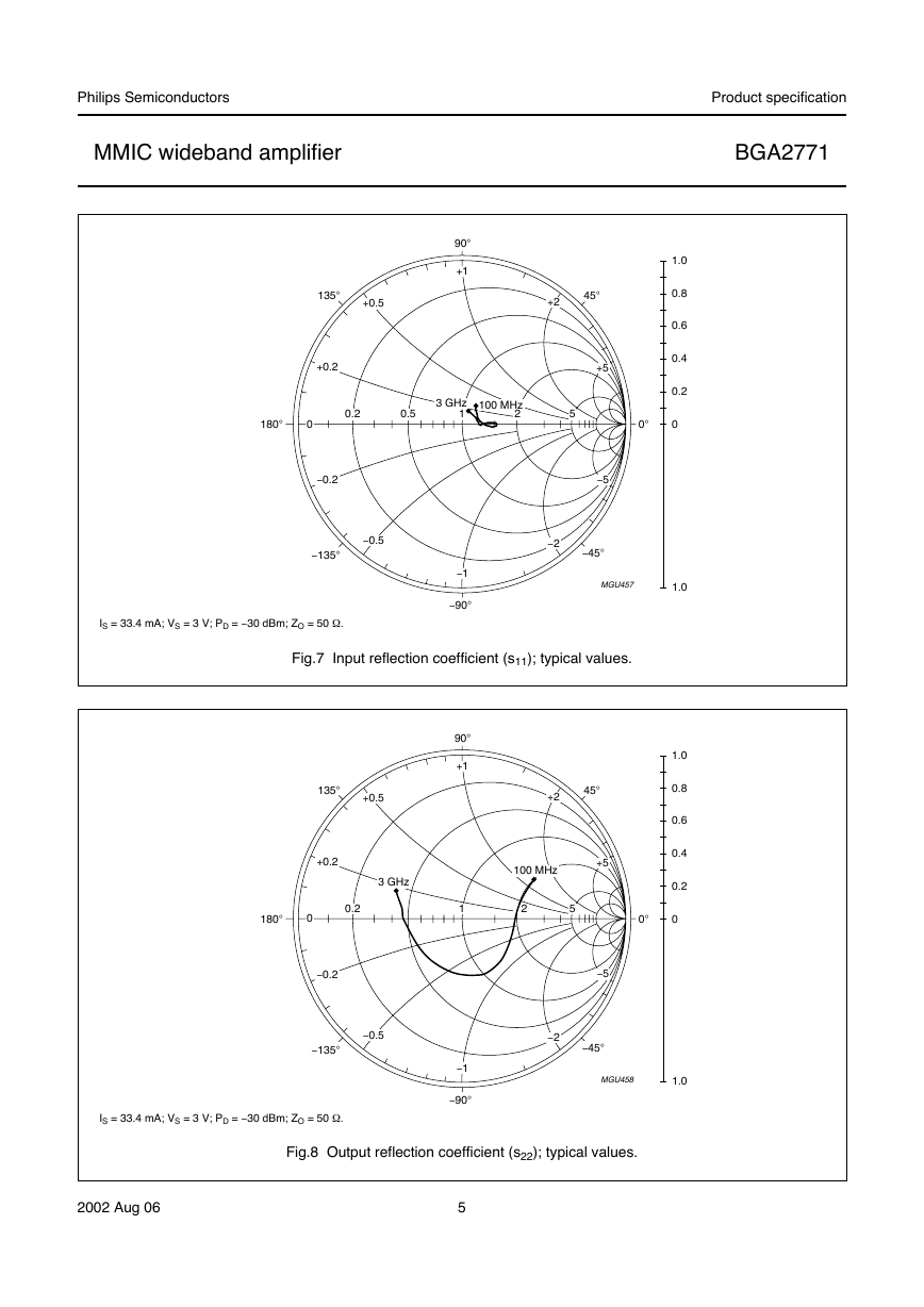
IS = 33.4 mA; VS = 3 V; PD = - 30 dBm; ZO = 50 W.
Fig.7 Input reflection coefficient (s11); typical values.
handbook, full pagewidth
90
+1
135
+0.5
45
+2
+0.2
3 GHz
100 MHz
180
0
0.2
1
2
5
1.0
0.8
0.6
0.4
0.2
0
+5
- 5
0
- 0.2
- 0.5
- 135
- 2
- 45
MGU458
1.0
- 1
- 90
IS = 33.4 mA; VS = 3 V; PD = - 30 dBm; ZO = 50 W.
Fig.8 Output reflection coefficient (s22); typical values.
2002 Aug 06
5
�
Philips Semiconductors
MMIC wideband amplifier
Product specification
BGA2771
handbook, halfpage
0
MGU459
handbook, halfpage
30
MGU460
2
s12
(dB)
- 20
- 40
- 60
0
1000
2000
3000
f (MHz)
2
s21
(dB)
20
10
0
0
1000
2000
3000
f (MHz)
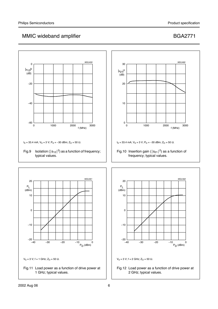
IS = 33.4 mA; VS = 3 V; PD = - 30 dBm; ZO = 50 W.
IS = 33.4 mA; VS = 3 V; PD = - 30 dBm; ZO = 50 W.
Fig.9
Isolation ( s12 2) as a function of frequency;
typical values.
Fig.10 Insertion gain ( s21 2) as a function of
frequency; typical values.
handbook, halfpage
20
MGU461
handbook, halfpage
20
MGU462
PL
(dBm)
10
0
- 10
PL
(dBm)
10
0
- 10
- 20
- 40
- 30
- 20
- 10
0
PD (dBm)
- 20
- 40
- 30
- 20
- 10
0
PD (dBm)
VS = 3 V; f = 1 GHz; ZO = 50 W.
VS = 3 V; f = 2 GHz; ZO = 50 W.
Fig.11 Load power as a function of drive power at
Fig.12 Load power as a function of drive power at
1 GHz; typical values.
2 GHz; typical values.
2002 Aug 06
6
�
Philips Semiconductors
MMIC wideband amplifier
Product specification
BGA2771
handbook, halfpage
10
NF
(dB)
8
6
4
2
0
0
MGU463
handbook, halfpage
5
MGU464
K
4
3
2
1
0
0
1000
2000
f (MHz)
3000
1000
2000
f (MHz)
3000
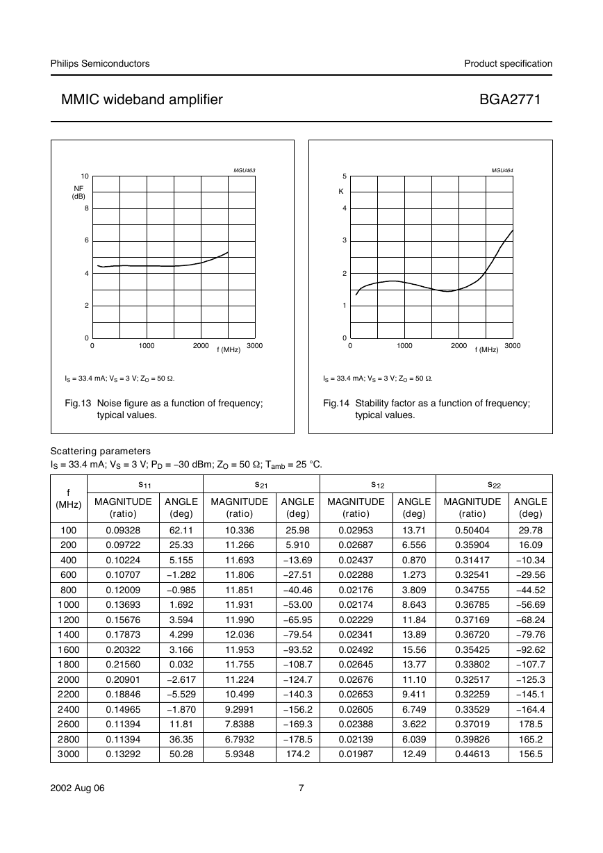
IS = 33.4 mA; VS = 3 V; ZO = 50 W.
IS = 33.4 mA; VS = 3 V; ZO = 50 W.
Fig.13 Noise figure as a function of frequency;
Fig.14 Stability factor as a function of frequency;
typical values.
typical values.
Scattering parameters
IS = 33.4 mA; VS = 3 V; PD = - 30 dBm; ZO = 50 W
; Tamb = 25 C.
s21
MAGNITUDE
f
(MHz)
100
200
400
600
800
1000
1200
1400
1600
1800
2000
2200
2400
2600
2800
3000
s11
MAGNITUDE
(ratio)
0.09328
0.09722
0.10224
0.10707
0.12009
0.13693
0.15676
0.17873
0.20322
0.21560
0.20901
0.18846
0.14965
0.11394
0.11394
0.13292
ANGLE
(deg)
62.11
25.33
5.155
- 1.282
- 0.985
1.692
3.594
4.299
3.166
0.032
- 2.617
- 5.529
- 1.870
11.81
36.35
50.28
s12
MAGNITUDE
(ratio)
0.02953
0.02687
0.02437
0.02288
0.02176
0.02174
0.02229
0.02341
0.02492
0.02645
0.02676
0.02653
0.02605
0.02388
0.02139
0.01987
ANGLE
(deg)
13.71
6.556
0.870
1.273
3.809
8.643
11.84
13.89
15.56
13.77
11.10
9.411
6.749
3.622
6.039
12.49
s22
MAGNITUDE
(ratio)
0.50404
0.35904
0.31417
0.32541
0.34755
0.36785
0.37169
0.36720
0.35425
0.33802
0.32517
0.32259
0.33529
0.37019
0.39826
0.44613
ANGLE
(deg)
29.78
16.09
- 10.34
- 29.56
- 44.52
- 56.69
- 68.24
- 79.76
- 92.62
- 107.7
- 125.3
- 145.1
- 164.4
178.5
165.2
156.5
ANGLE
(deg)
25.98
5.910
- 13.69
- 27.51
- 40.46
- 53.00
- 65.95
- 79.54
- 93.52
- 108.7
- 124.7
- 140.3
- 156.2
- 169.3
- 178.5
174.2
(ratio)
10.336
11.266
11.693
11.806
11.851
11.931
11.990
12.036
11.953
11.755
11.224
10.499
9.2991
7.8388
6.7932
5.9348
2002 Aug 06
7
�
Philips Semiconductors
MMIC wideband amplifier
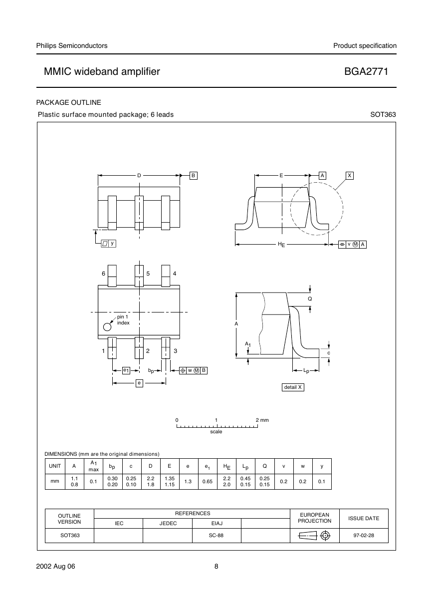
PACKAGE OUTLINE
Plastic surface mounted package; 6 leads
Product specification
BGA2771
SOT363
D
B
E
A
X
y
6
1
5
4
pin 1
index
2
bp
e1
e
w
BM
3
0
HE
v M A
A
A1
Q
c
Lp
detail X
1
scale
2 mm
DIMENSIONS (mm are the original dimensions)
UNIT
mm
A
1.1
0.8
A1
max
0.1
bp
0.30
0.20
c
0.25
0.10
D
2.2
1.8
E
e
e1
1.35
1.15
1.3
0.65
HE
2.2
2.0
Lp
0.45
0.15
Q
v
w
y
0.25
0.15
0.2
0.2
0.1
OUTLINE
VERSION
SOT363
2002 Aug 06
REFERENCES
IEC
JEDEC
EIAJ
SC-88
8
EUROPEAN
PROJECTION
ISSUE DATE
97-02-28
�



 2023年江西萍乡中考道德与法治真题及答案.doc
 2012年重庆南川中考生物真题及答案.doc
 2013年江西师范大学地理学综合及文艺理论基础考研真题.doc
 2020年四川甘孜小升初语文真题及答案I卷.doc
 2020年注册岩土工程师专业基础考试真题及答案.doc
 2023-2024学年福建省厦门市九年级上学期数学月考试题及答案.doc
 2021-2022学年辽宁省沈阳市大东区九年级上学期语文期末试题及答案.doc
 2022-2023学年北京东城区初三第一学期物理期末试卷及答案.doc
 2018上半年江西教师资格初中地理学科知识与教学能力真题及答案.doc
 2012年河北国家公务员申论考试真题及答案-省级.doc
 2020-2021学年江苏省扬州市江都区邵樊片九年级上学期数学第一次质量检测试题及答案.doc
 2022下半年黑龙江教师资格证中学综合素质真题及答案.doc