環天衛星科技股份有限公司
PRODUCT USER MANUAL
GPS ENGINE BOARD
ET-314
GlobalSat Technology Corporation
台北縣中和市建一路 186 號 16 樓(遠東世紀廣場)
16, No.186,Chien 1 Road, 235Chung Ho City,Taipei Hsien, Taiwan ,R.O.C.
Tel: 886-2-8226-3799(Rep.) Fax: 886-2-8226-3899
Web: www.globalsat.com.tw E-mail: service@globalsat.com.tw
�
SiRF StarⅢ
L1, 1575.42 MHz
1.023 MHz chip rate
20 channel all-in-view tracking
-159 dBm
Features:
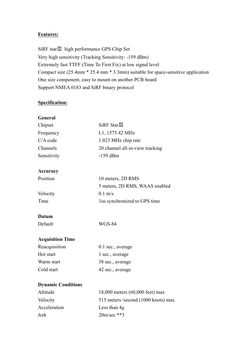
SiRF starⅢ high performance GPS Chip Set
Very high sensitivity (Tracking Sensitivity: -159 dBm)
Extremely fast TTFF (Time To First Fix) at low signal level
Compact size (25.4mm * 25.4 mm * 3.3mm) suitable for space-sensitive application
One size component, easy to mount on another PCB board
Support NMEA 0183 and SiRF binary protocol
Specification:
General
Chipset
Frequency
C/A code
Channels
Sensitivity
Accuracy
Position
Velocity
Time
Datum
Default
Acquisition Time
Reacquisition
Hot start
Warm start
Cold start
Dynamic Conditions
Altitude
Velocity
Acceleration
Jerk
18,000 meters (60,000 feet) max
515 meters /second (1000 knots) max
Less than 4g
20m/sec **3
10 meters, 2D RMS
5 meters, 2D RMS, WAAS enabled
0.1 m/s
1us synchronized to GPS time
0.1 sec., average
1 sec., average
38 sec., average
42 sec., average
WGS-84
�
Power
Main power input
Power consumption
Interface
Dimension
Baud rate
Output message
3.3V +- 5% DC input
68mA (Continuous mode)
25.4mm * 25.4 mm * 3.3mm
4,800 to 57,600 bps adjustable
SiRF binary or
NMEA 0183 GGA, GSA, GSV, RMC, VTG, GLL
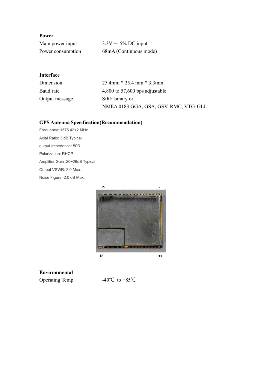
GPS Antenna Specification(Recommendation)
Frequency: 1575.42+2 MHz
Axial Ratio: 3 dB Typical
output Impedance: 50Ω
Polarization: RHCP
Amplifier Gain :20~26dB Typical
Output VSWR: 2.0 Max.
Noise Figure: 2.0 dB Max.
Environmental
Operating Temp
-40℃ to +85℃
�
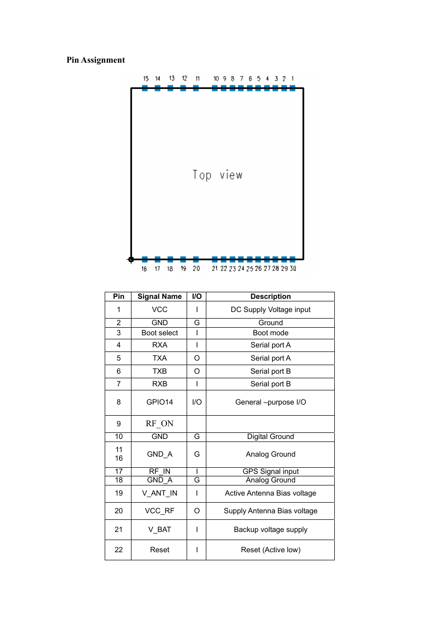
Pin Assignment
Pin
1
2
3
4
5
6
7
8
9
10
11
16
17
18
19
20
21
22
Signal Name
VCC
GND
Boot select
RXA
TXA
TXB
RXB
GPIO14
RF_ON
GND
GND_A
RF_IN
GND_A
V_ANT_IN
VCC_RF
V_BAT
Reset
I/O
I
G
I
I
O
O
I
I/O
G
G
I
G
I
O
I
I
Description
DC Supply Voltage input
Ground
Boot mode
Serial port A
Serial port A
Serial port B
Serial port B
General –purpose I/O
Digital Ground
Analog Ground
GPS Signal input
Analog Ground
Active Antenna Bias voltage
Supply Antenna Bias voltage
Backup voltage supply
Reset (Active low)
�
23
24
25
26
27
28
29
30
GPIO10
GPIO1
GPIO5
GPIO0
GPIO13
GPIO15
PPS
GND
I/O
I/O
I/O
I/O
I/O
I/O
O
G
General purpose I/O
General purpose I/O
General purpose I/O
General purpose I/O
(support continuous power mode only)
General purpose I/O
General purpose I/O
One pulse per second
Digital Ground
Definition of Pin assignment
VCC
This is the main DC supply for a 3.3V +- 5% DC input power module board.
GND
GND provides the ground for digital part.
Boot select
Set this pin to high for programming flash.
RXA
This is the main receiver channel and is used to receive software commands to
the board from SIRFdemo software or from user written software.
PS: Pull up if not used.
RXB
This is the auxiliary receiving channel and is used to input differential
corrections to the board to enable DGPS navigation.
PS: Pull up if not used.
TXA
This is the main transmitting channel and is used to output
navigation and measurement data to SiRFdemo or user written software.
�
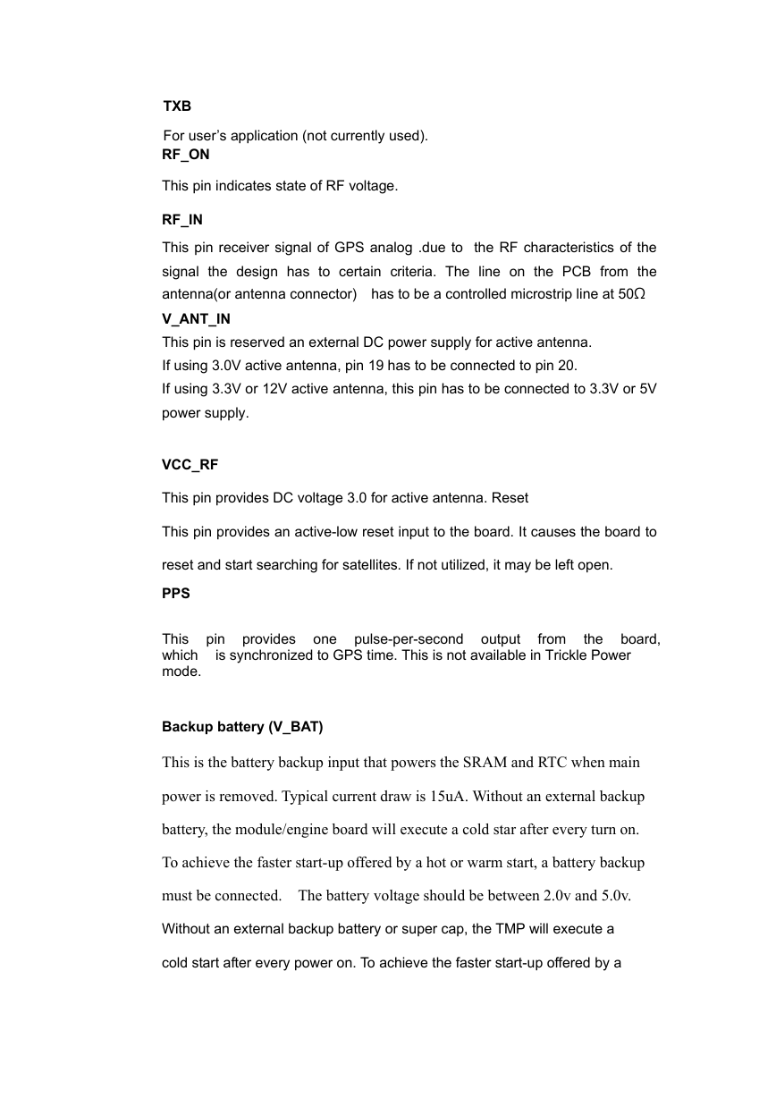
TXB
For user’s application (not currently used).
RF_ON
This pin indicates state of RF voltage.
RF_IN
This pin receiver signal of GPS analog .due to the RF characteristics of the
signal the design has to certain criteria. The line on the PCB from the
antenna(or antenna connector) has to be a controlled microstrip line at 50Ω
V_ANT_IN
This pin is reserved an external DC power supply for active antenna.
If using 3.0V active antenna, pin 19 has to be connected to pin 20.
If using 3.3V or 12V active antenna, this pin has to be connected to 3.3V or 5V
power supply.
VCC_RF
This pin provides DC voltage 3.0 for active antenna. Reset
This pin provides an active-low reset input to the board. It causes the board to
reset and start searching for satellites. If not utilized, it may be left open.
PPS
This pin provides one pulse-per-second output from the board,
which is synchronized to GPS time. This is not available in Trickle Power
mode.
Backup battery (V_BAT)
This is the battery backup input that powers the SRAM and RTC when main
power is removed. Typical current draw is 15uA. Without an external backup
battery, the module/engine board will execute a cold star after every turn on.
To achieve the faster start-up offered by a hot or warm start, a battery backup
must be connected. The battery voltage should be between 2.0v and 5.0v.
Without an external backup battery or super cap, the TMP will execute a
cold start after every power on. To achieve the faster start-up offered by a
�
hot or warm start, either a battery backup must be connected or a super
cap installed.
To maximize battery lifetime, the battery voltage should not exceed the
supply voltage and should be between 2.5V and 3.6V.
With the super cap (B1) installed, and after at least ten minutes of
continuous operation, the data retention is about seven hours.
Note that even though all other components are rated at –30 to +85 deg C, a
typical super cap is specified over a temperature range of –25 to +70 deg C
and a typical rechargeable Lithium battery is over –20 to +70 deg C.
GPIO Functions
Several I/Os are connected to the digital interface connector
for custom applications.
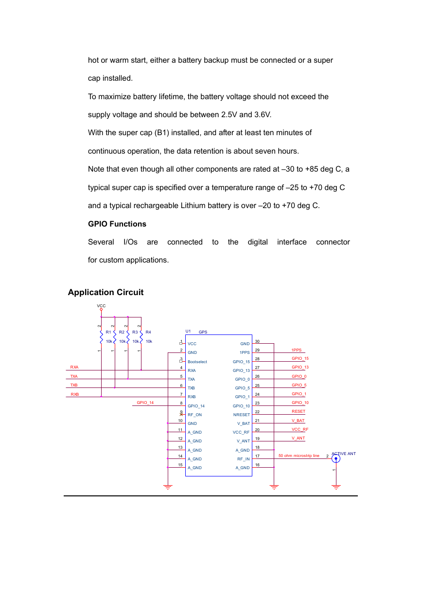
Application Circuit
VCC
2
2
2
2
R1
10k
R2
10k
R3
10k
R4
10k
1
1
1
1
GPIO_14
U1
GPS
VCC
GND
Bootselect
RXA
TXA
TXB
RXB
GPIO_14
RF_ON
GND
A_GND
A_GND
A_GND
A_GND
A_GND
1
2
3
4
5
6
7
8
9
10
11
12
13
14
15
GND
1PPS
GPIO_15
GPIO_13
GPIO_0
GPIO_5
GPIO_1
GPIO_10
NRESET
V_BAT
VCC_RF
V_ANT
A_GND
RF_IN
A_GND
30
29
28
27
26
25
24
23
22
21
20
19
18
17
16
1PPS
GPIO_15
GPIO_13
GPIO_0
GPIO_5
GPIO_1
GPIO_10
RESET
V_BAT
VCC_RF
V_ANT
50 ohm microstrip line
2
ACTIVE ANT
1
RXA
TXA
TXB
RXB
�
(1) Ground Planes:
ET-314 GPS receiver needs two different ground planes. The GND_A pin(11、
12、13、14、15、16、18) shall be connect to analog ground.
The GND pin(2、10、30) connect to digital ground.
(2) Serial Interface:
The Serial interface pin(RXA、TX1、TXB、RXB) is recommended to pull up(10KΩ).
It can increase the stability of serial data.
(3) Backup Battery:
It’s recommended to connect a backup battery to V_BAT.
In order to enable the warm and hot start features of the GPS receiver. If you
don’t intend to use a backup battery, connect this pin to GND or open.
If you use backup battery, shall need to add a bypassing capacitor (10uF) at
V_bat trace. It can reduce noise and increase the stability.
(4) Antenna:
Connecting to the antenna has to be routed on the PCB. The transmission line
must to controlled impedance to connect RF_IN to the antenna or antenna
connector of your choice.
(5) Active antenna bias voltage:
The Vcc_RF pin (pin 20) is providing voltage 3.3V. If you use active antenna,
you can connect this pin to V_ANT_IN pin (pin 19) to provide bias voltage of
active
�




 2023年江西萍乡中考道德与法治真题及答案.doc
 2012年重庆南川中考生物真题及答案.doc
 2013年江西师范大学地理学综合及文艺理论基础考研真题.doc
 2020年四川甘孜小升初语文真题及答案I卷.doc
 2020年注册岩土工程师专业基础考试真题及答案.doc
 2023-2024学年福建省厦门市九年级上学期数学月考试题及答案.doc
 2021-2022学年辽宁省沈阳市大东区九年级上学期语文期末试题及答案.doc
 2022-2023学年北京东城区初三第一学期物理期末试卷及答案.doc
 2018上半年江西教师资格初中地理学科知识与教学能力真题及答案.doc
 2012年河北国家公务员申论考试真题及答案-省级.doc
 2020-2021学年江苏省扬州市江都区邵樊片九年级上学期数学第一次质量检测试题及答案.doc
 2022下半年黑龙江教师资格证中学综合素质真题及答案.doc