U
s
e
r
’
s
M
a
n
u
a
l
RL78 Family
User’s Manual: Software
Single-Chip Microcontrollers
All information contained in these materials, including products and product specifications,
represents information on the product at the time of publication and is subject to change by
Renesas Electronics Corp. without notice. Please review the latest information published by
Renesas Electronics Corp. through various means, including the Renesas Electronics Corp.
website (http://www.renesas.com).
www.renesas.com
Rev.2.10 Jan 2014
�
Notice
1. Descriptions of circuits, software and other related information in this document are provided only to illustrate the operation of
semiconductor products and application examples. You are fully responsible for the incorporation of these circuits, software,
and information in the design of your equipment. Renesas Electronics assumes no responsibility for any losses incurred by you
or third parties arising from the use of these circuits, software, or information.
2. Renesas Electronics has used reasonable care in preparing the information included in this document, but Renesas Electronics
does not warrant that such information is error free. Renesas Electronics assumes no liability whatsoever for any damages
incurred by you resulting from errors in or omissions from the information included herein.
3. Renesas Electronics does not assume any liability for infringement of patents, copyrights, or other intellectual property rights of
third parties by or arising from the use of Renesas Electronics products or technical information described in this document. No
license, express, implied or otherwise, is granted hereby under any patents, copyrights or other intellectual property rights of
Renesas Electronics or others.
4. You should not alter, modify, copy, or otherwise misappropriate any Renesas Electronics product, whether in whole or in part.
Renesas Electronics assumes no responsibility for any losses incurred by you or third parties arising from such alteration,
modification, copy or otherwise misappropriation of Renesas Electronics product.
5. Renesas Electronics products are classified according to the following two quality grades: “Standard” and “High Quality”. The
recommended applications for each Renesas Electronics product depends on the product’s quality grade, as indicated below.
Computers; office equipment; communications equipment; test and measurement equipment; audio and visual
“Standard”:
equipment; home electronic appliances; machine tools; personal electronic equipment; and industrial robots etc.
“High Quality”: Transportation equipment (automobiles, trains, ships, etc.); traffic control systems; anti-disaster systems; anti-
crime systems; and safety equipment etc.
Renesas Electronics products are neither intended nor authorized for use in products or systems that may pose a direct threat to
human life or bodily injury (artificial life support devices or systems, surgical implantations etc.), or may cause serious property
damages (nuclear reactor control systems, military equipment etc.). You must check the quality grade of each Renesas
Electronics product before using it in a particular application. You may not use any Renesas Electronics product for any
application for which it is not intended. Renesas Electronics shall not be in any way liable for any damages or losses incurred
by you or third parties arising from the use of any Renesas Electronics product for which the product is not intended by Renesas
Electronics.
6. You should use the Renesas Electronics products described in this document within the range specified by Renesas Electronics,
especially with respect to the maximum rating, operating supply voltage range, movement power voltage range, heat radiation
characteristics, installation and other product characteristics. Renesas Electronics shall have no liability for malfunctions or
damages arising out of the use of Renesas Electronics products beyond such specified ranges.
7. Although Renesas Electronics endeavors to improve the quality and reliability of its products, semiconductor products have
specific characteristics such as the occurrence of failure at a certain rate and malfunctions under certain use conditions. Further,
Renesas Electronics products are not subject to radiation resistance design. Please be sure to implement safety measures to
guard them against the possibility of physical injury, and injury or damage caused by fire in the event of the failure of a Renesas
Electronics product, such as safety design for hardware and software including but not limited to redundancy, fire control and
malfunction prevention, appropriate treatment for aging degradation or any other appropriate measures. Because the evaluation
of microcomputer software alone is very difficult, please evaluate the safety of the final products or systems manufactured by
you.
8. Please contact a Renesas Electronics sales office for details as to environmental matters such as the environmental compatibility
of each Renesas Electronics product. Please use Renesas Electronics products in compliance with all applicable laws and
regulations that regulate the inclusion or use of controlled substances, including without limitation, the EU RoHS Directive.
Renesas Electronics assumes no liability for damages or losses occurring as a result of your noncompliance with applicable laws
and regulations.
9. Renesas Electronics products and technology may not be used for or incorporated into any products or systems whose
manufacture, use, or sale is prohibited under any applicable domestic or foreign laws or regulations. You should not use
Renesas Electronics products or technology described in this document for any purpose relating to military applications or use
by the military, including but not limited to the development of weapons of mass destruction. When exporting the Renesas
Electronics products or technology described in this document, you should comply with the applicable export control laws and
regulations and follow the procedures required by such laws and regulations.
10. It is the responsibility of the buyer or distributor of Renesas Electronics products, who distributes, disposes of, or otherwise
places the product with a third party, to notify such third party in advance of the contents and conditions set forth in this
document, Renesas Electronics assumes no responsibility for any losses incurred by you or third parties as a result of
unauthorized use of Renesas Electronics products.
11. This document may not be reproduced or duplicated in any form, in whole or in part, without prior written consent of Renesas
Electronics.
12. Please contact a Renesas Electronics sales office if you have any questions regarding the information contained in this document
or Renesas Electronics products, or if you have any other inquiries.
(Note 1) “Renesas Electronics” as used in this document means Renesas Electronics Corporation and also includes its majority-
owned subsidiaries.
(Note 2) “Renesas Electronics product(s)” means any product developed or manufactured by or for Renesas Electronics.
(2012.4)
�
NOTES FOR CMOS DEVICES
(1) VOLTAGE APPLICATION WAVEFORM AT INPUT PIN: Waveform distortion due to input noise or a
reflected wave may cause malfunction. If the input of the CMOS device stays in the area between VIL
(MAX) and VIH (MIN) due to noise, etc., the device may malfunction. Take care to prevent chattering noise
from entering the device when the input level is fixed, and also in the transition period when the input level
passes through the area between VIL (MAX) and VIH (MIN).
(2) HANDLING OF UNUSED INPUT PINS: Unconnected CMOS device inputs can be cause of malfunction. If
an input pin is unconnected, it is possible that an internal input level may be generated due to noise, etc.,
causing malfunction. CMOS devices behave differently than Bipolar or NMOS devices. Input levels of
CMOS devices must be fixed high or low by using pull-up or pull-down circuitry. Each unused pin should be
connected to VDD or GND via a resistor if there is a possibility that it will be an output pin. All handling
related to unused pins must be judged separately for each device and according to related specifications
governing the device.
(3) PRECAUTION AGAINST ESD: A strong electric field, when exposed to a MOS device, can cause
destruction of the gate oxide and ultimately degrade the device operation. Steps must be taken to stop
generation of static electricity as much as possible, and quickly dissipate it when it has occurred.
Environmental control must be adequate. When it is dry, a humidifier should be used. It is recommended
to avoid using insulators that easily build up static electricity. Semiconductor devices must be stored and
transported in an anti-static container, static shielding bag or conductive material. All test and measurement
tools including work benches and floors should be grounded. The operator should be grounded using a wrist
strap. Semiconductor devices must not be touched with bare hands. Similar precautions need to be taken
for PW boards with mounted semiconductor devices.
(4) STATUS BEFORE INITIALIZATION: Power-on does not necessarily define the initial status of a MOS
device. Immediately after the power source is turned ON, devices with reset functions have not yet been
initialized. Hence, power-on does not guarantee output pin levels, I/O settings or contents of registers. A
device is not initialized until the reset signal is received. A reset operation must be executed immediately
after power-on for devices with reset functions.
(5) POWER ON/OFF SEQUENCE: In the case of a device that uses different power supplies for the internal
operation and external interface, as a rule, switch on the external power supply after switching on the internal
power supply. When switching the power supply off, as a rule, switch off the external power supply and then
the internal power supply. Use of the reverse power on/off sequences may result in the application of an
overvoltage to the internal elements of the device, causing malfunction and degradation of internal elements
due to the passage of an abnormal current. The correct power on/off sequence must be judged separately
for each device and according to related specifications governing the device.
(6) INPUT OF SIGNAL DURING POWER OFF STATE : Do not input signals or an I/O pull-up power supply
while the device is not powered. The current injection that results from input of such a signal or I/O pull-up
power supply may cause malfunction and the abnormal current that passes in the device at this time may
cause degradation of internal elements. Input of signals during the power off state must be judged
separately for each device and according to related specifications governing the device.
�
Target Readers
Purpose
Organization
How to Read This Manual
Conventions
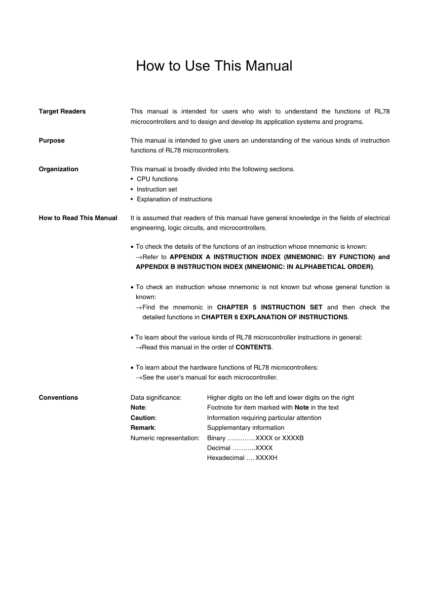
How to Use This Manual
This manual is intended for users who wish to understand the functions of RL78
microcontrollers and to design and develop its application systems and programs.
This manual is intended to give users an understanding of the various kinds of instruction
functions of RL78 microcontrollers.
This manual is broadly divided into the following sections.
• CPU functions
Instruction set
Explanation of instructions
It is assumed that readers of this manual have general knowledge in the fields of electrical
engineering, logic circuits, and microcontrollers.
• To check the details of the functions of an instruction whose mnemonic is known:
→ Refer to APPENDIX A INSTRUCTION INDEX (MNEMONIC: BY FUNCTION) and
APPENDIX B INSTRUCTION INDEX (MNEMONIC: IN ALPHABETICAL ORDER).
• To check an instruction whose mnemonic is not known but whose general function is
known:
→ Find the mnemonic in CHAPTER 5 INSTRUCTION SET and then check the
detailed functions in CHAPTER 6 EXPLANATION OF INSTRUCTIONS.
• To learn about the various kinds of RL78 microcontroller instructions in general:
→Read this manual in the order of CONTENTS.
• To learn about the hardware functions of RL78 microcontrollers:
→ See the user’s manual for each microcontroller.
Data significance:
Note:
Caution:
Remark:
Numeric representation: Binary …………. XXXX or XXXXB
Higher digits on the left and lower digits on the right
Footnote for item marked with Note in the text
Information requiring particular attention
Supplementary information
Decimal ……….. XXXX
Hexadecimal …. XXXXH
�
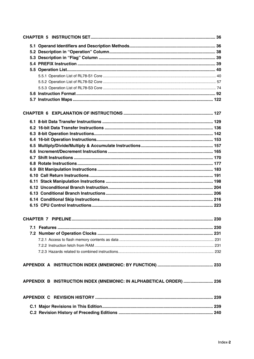
CONTENTS
CHAPTER 1 OVERVIEW......................................................................................................................... 1
1.1 Features ........................................................................................................................................ 1
1.2 Functional Differences between Three CPU Cores .................................................................. 2
CHAPTER 2 MEMORY SPACE............................................................................................................... 3
2.1 Memory Space.............................................................................................................................. 3
2.2 Internal Program Memory Space................................................................................................ 5
2.2.1 Mirror area............................................................................................................................................ 5
2.2.2 Vector table area .................................................................................................................................. 7
2.2.3 CALLT instruction table area ................................................................................................................ 7
2.2.4 Option byte area ................................................................................................................................... 7
2.2.5 On-chip debug security ID setting area ................................................................................................ 7
2.3 Internal Data Memory (Internal RAM) Space ............................................................................. 8
2.4 Special Function Register (SFR) Area ....................................................................................... 9
2.5 Extended SFR (Second SFR) Area ............................................................................................. 9
CHAPTER 3 REGISTERS ..................................................................................................................... 10
3.1 Control Registers ....................................................................................................................... 10
3.1.1 Program counter (PC) ........................................................................................................................ 10
3.1.2 Program status word (PSW)............................................................................................................... 10
3.1.3 Stack pointer (SP) .............................................................................................................................. 11
3.2 General-Purpose Registers....................................................................................................... 13
3.2.1 General-purpose registers of RL78-S1 core....................................................................................... 13
3.2.2 General-purpose registers of RL78-S2 core and RL78-S3 core......................................................... 13
3.3 ES and CS Registers.................................................................................................................. 16
3.4 Special Function Registers (SFRs) .......................................................................................... 17
3.4.1 Processor mode control register (PMC) ............................................................................................. 17
CHAPTER 4 ADDRESSING .................................................................................................................. 19
4.1 Instruction Address Addressing .............................................................................................. 19
4.1.1 Relative addressing ............................................................................................................................ 19
4.1.2 Immediate addressing ........................................................................................................................ 20
4.1.3 Table indirect addressing ................................................................................................................... 20
4.1.4 Register direct addressing.................................................................................................................. 21
4.2 Addressing for Processing Data Addresses........................................................................... 22
4.2.1 Implied addressing ............................................................................................................................. 22
4.2.2 Register addressing............................................................................................................................ 22
4.2.3 Direct addressing................................................................................................................................ 23
4.2.4 Short direct addressing....................................................................................................................... 24
4.2.5 SFR addressing.................................................................................................................................. 25
4.2.6 Register indirect addressing ............................................................................................................... 26
4.2.7 Based addressing............................................................................................................................... 27
4.2.8 Based indexed addressing ................................................................................................................. 31
4.2.9 Stack addressing ................................................................................................................................ 32
Index-1
�
CHAPTER 5 INSTRUCTION SET.......................................................................................................... 36
5.1 Operand Identifiers and Description Methods......................................................................... 36
5.2 Description in “Operation” Column.......................................................................................... 38
5.3 Description in “Flag” Column ................................................................................................... 39
5.4 PREFIX Instruction ..................................................................................................................... 39
5.5 Operation List.............................................................................................................................. 40
5.5.1 Operation List of RL78-S1 Core ......................................................................................................... 40
5.5.2 Operation List of RL78-S2 Core ......................................................................................................... 57
5.5.3 Operation List of RL78-S3 Core ......................................................................................................... 74
5.6 Instruction Format ...................................................................................................................... 92
5.7 Instruction Maps ....................................................................................................................... 122
CHAPTER 6 EXPLANATION OF INSTRUCTIONS ............................................................................ 127
6.1 8-bit Data Transfer Instructions .............................................................................................. 129
6.2 16-bit Data Transfer Instructions ............................................................................................ 136
6.3 8-bit Operation Instructions..................................................................................................... 142
6.4 16-bit Operation Instructions................................................................................................... 153
6.5 Multiply/Divide/Multiply & Accumulate Instructions............................................................. 157
6.6 Increment/Decrement Instructions ......................................................................................... 165
6.7 Shift Instructions ...................................................................................................................... 170
6.8 Rotate Instructions ................................................................................................................... 177
6.9 Bit Manipulation Instructions .................................................................................................. 183
6.10 Call Return Instructions ......................................................................................................... 191
6.11 Stack Manipulation Instructions ........................................................................................... 198
6.12 Unconditional Branch Instruction......................................................................................... 204
6.13 Conditional Branch Instructions........................................................................................... 206
6.14 Conditional Skip Instructions................................................................................................ 216
6.15 CPU Control Instructions....................................................................................................... 223
CHAPTER 7 PIPELINE........................................................................................................................ 230
7.1 Features .................................................................................................................................... 230
7.2 Number of Operation Clocks .................................................................................................. 231
7.2.1 Access to flash memory contents as data ........................................................................................ 231
7.2.2 Instruction fetch from RAM ............................................................................................................... 231
7.2.3 Hazards related to combined instructions......................................................................................... 232
APPENDIX A INSTRUCTION INDEX (MNEMONIC: BY FUNCTION) ............................................... 233
APPENDIX B INSTRUCTION INDEX (MNEMONIC: IN ALPHABETICAL ORDER) ......................... 236
APPENDIX C REVISION HISTORY .................................................................................................... 239
C.1 Major Revisions in This Edition.............................................................................................. 239
C.2 Revision History of Preceding Editions ................................................................................ 240
Index-2
�
RL78 Family
RENESAS MCU
R01US0015EJ0210
Rev.2.10
Jan 27, 2014
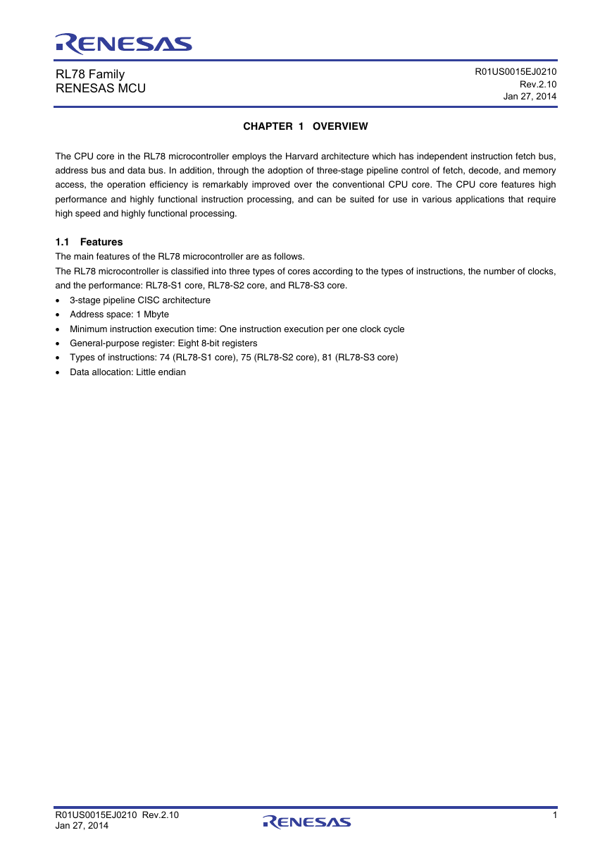
CHAPTER 1 OVERVIEW
The CPU core in the RL78 microcontroller employs the Harvard architecture which has independent instruction fetch bus,
address bus and data bus. In addition, through the adoption of three-stage pipeline control of fetch, decode, and memory
access, the operation efficiency is remarkably improved over the conventional CPU core. The CPU core features high
performance and highly functional instruction processing, and can be suited for use in various applications that require
high speed and highly functional processing.
1.1 Features
The main features of the RL78 microcontroller are as follows.
The RL78 microcontroller is classified into three types of cores according to the types of instructions, the number of clocks,
and the performance: RL78-S1 core, RL78-S2 core, and RL78-S3 core.
3-stage pipeline CISC architecture
Address space: 1 Mbyte
Minimum instruction execution time: One instruction execution per one clock cycle
General-purpose register: Eight 8-bit registers
Types of instructions: 74 (RL78-S1 core), 75 (RL78-S2 core), 81 (RL78-S3 core)
Data allocation: Little endian
R01US0015EJ0210 Rev.2.10
Jan 27, 2014
1
�
RL78 Family
CHAPTER 1 OUTLINE
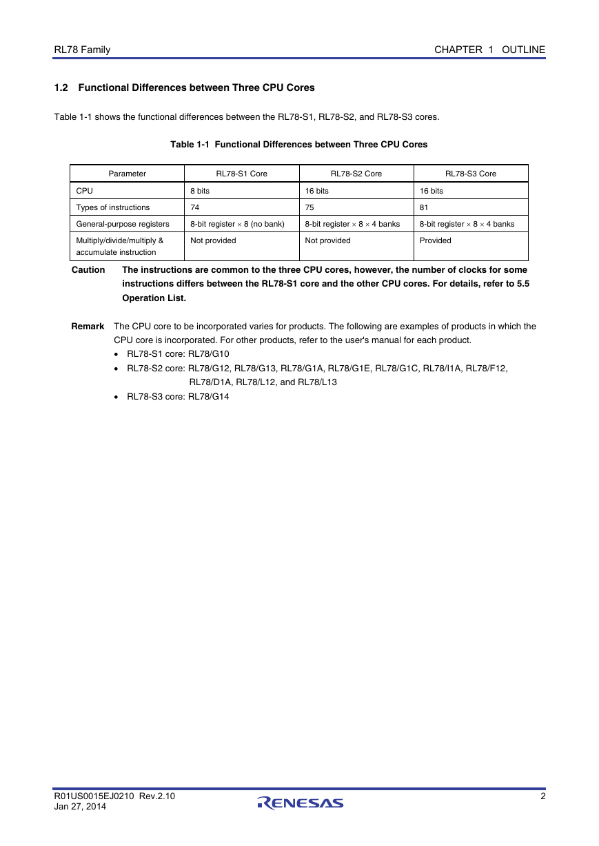
1.2 Functional Differences between Three CPU Cores
Table 1-1 shows the functional differences between the RL78-S1, RL78-S2, and RL78-S3 cores.
Table 1-1 Functional Differences between Three CPU Cores
Parameter
RL78-S1 Core
RL78-S2 Core
RL78-S3 Core
CPU
Types of instructions
8 bits
74
16 bits
75
16 bits
81
General-purpose registers
8-bit register 8 (no bank)
8-bit register 8 4 banks
8-bit register 8 4 banks
Multiply/divide/multiply &
accumulate instruction
Not provided
Not provided
Provided
Caution
The instructions are common to the three CPU cores, however, the number of clocks for some
instructions differs between the RL78-S1 core and the other CPU cores. For details, refer to 5.5
Operation List.
Remark The CPU core to be incorporated varies for products. The following are examples of products in which the
CPU core is incorporated. For other products, refer to the user's manual for each product.
RL78-S1 core: RL78/G10
RL78-S2 core: RL78/G12, RL78/G13, RL78/G1A, RL78/G1E, RL78/G1C, RL78/I1A, RL78/F12,
RL78-S3 core: RL78/G14
RL78/D1A, RL78/L12, and RL78/L13
R01US0015EJ0210 Rev.2.10
Jan 27, 2014
2
�



 2023年江西萍乡中考道德与法治真题及答案.doc
 2012年重庆南川中考生物真题及答案.doc
 2013年江西师范大学地理学综合及文艺理论基础考研真题.doc
 2020年四川甘孜小升初语文真题及答案I卷.doc
 2020年注册岩土工程师专业基础考试真题及答案.doc
 2023-2024学年福建省厦门市九年级上学期数学月考试题及答案.doc
 2021-2022学年辽宁省沈阳市大东区九年级上学期语文期末试题及答案.doc
 2022-2023学年北京东城区初三第一学期物理期末试卷及答案.doc
 2018上半年江西教师资格初中地理学科知识与教学能力真题及答案.doc
 2012年河北国家公务员申论考试真题及答案-省级.doc
 2020-2021学年江苏省扬州市江都区邵樊片九年级上学期数学第一次质量检测试题及答案.doc
 2022下半年黑龙江教师资格证中学综合素质真题及答案.doc