1 Scope
2 DDR4 SDRAM Package Pinout and Addressing
2.1 DDR4 SDRAM Row for X4, X8 and X16
2.2 DDR4 SDRAM Ball Pitch
2.3 .DDR4 SDRAM Columns for X4,X8 and X16
2.4 DDR4 SDRAM X4/8 Ballout using MO-207
2.5 DDR4 SDRAM X16 Ballout using MO-207
2.6 Pinout Description
2.7 DDR4 SDRAM Addressing
3 Functional Description
3.1 Simplified State Diagram
3.2 Basic Functionality
3.3 RESET and Initialization Procedure
3.3.1 Power-up Initialization Sequence
3.3.2 Reset Initialization with Stable Power
3.4 Register Definition
3.4.1 Programming the mode registers
3.5 Mode Register
4 DDR4 SDRAM Command Description and Operation
4.1 Command Truth Table
4.2 CKE Truth Table
4.3 Burst Length, Type and Order
4.3.1 BL8 Burst order with CRC Enabled
4.4 DLL-off Mode & DLL on/off Switching procedure
4.4.1 DLL on/off switching procedure
4.4.2 DLL “on” to DLL “off” Procedure
4.4.3 DLL “off” to DLL “on” Procedure
4.5 DLL-off Mode
4.6 Input Clock Frequency Change
4.7 Write Leveling
4.7.1 RAM setting for write leveling & DRAM termination function in that mode
4.7.2 Procedure Description
4.7.3 Write Leveling Mode Exit
1. After the last rising strobe edge (see ~T0), stop driving the strobe signals (see ~Tc0). Note: From now on, DQ pins are in undefined driving mode, and will remain undefined, until tMOD after the respective MRS command (Te1).
2. Drive ODT pin low (tIS must be satisfied) and continue registering low. (see Tb0).
3. After the RTT is switched off, disable Write Level Mode via MRS command (see Tc2).
4. After tMOD is satisfied (Te1), any valid command may be registered. (MRS commands may be issued after tMRD (Td1).
4.8 Temperature controlled Refresh modes
4.8.1 Normal temperature mode
4.8.2 Extended temperature mode
4.9 Fine Granularity Refresh Mode
4.9.1 Mode Register and Command Truth Table
4.9.2 tREFI and tRFC parameters
4.9.3 Changing Refresh Rate
4.9.4 Usage with Temperature Controlled Refresh mode
4.9.5 Self Refresh entry and exit
4.10 Multi Purpose Register
4.10.1 DQ Training with MPR
4.10.2 MR3 definition
4.10.3 MPR Reads
4.10.4 MPR Writes
4.10.5 MPR Read Data format
4.11 Data Mask(DM), Data Bus Inversion (DBI) and TDQS
4.12 ZQ Calibration Commands
4.12.1 ZQ Calibration Description
4.13 DQ Vref Training
4.14 Per DRAM Addressability
4.15 CAL Mode (CS_n to Command Address Latency)
4.15.1 CAL Mode Description
4.16 CRC
4.16.1 CRC Polynomial and logic equation
4.16.2 CRC data bit mapping for x8 devices
4.16.3 CRC data bit mapping for x4 devices
4.16.4 CRC data bit mapping for x16 devices
4.16.5 Write CRC for x4, x8 and x16 devices
4.16.6 RC Error Handling
4.16.7 CRC Frame format with BC4
4.16.8 Simultaneous DM and CRC Functionality
4.17 Command Address Parity( CA Parity )
4.17.1 CA Parity Error Log Readout
4.18 Control Gear Down Mode
4.19 DDR4 Key Core Timing
4.20 Programmable Preamble
4.20.1 Write Preamble
4.20.2 Read Preamble
4.20.3 Read Preamble Training
4.21 Postamble
4.21.1 Read Postamble
4.21.2 Write Postamble
4.22 ACTIVATE Command
4.23 Precharge Command
4.24 Read Operation
4.24.1 READ Timing Definitions
4.24.1.1 READ Timing; Clock to Data Strobe relationship
4.24.1.2 READ Timing; Data Strobe to Data relationship
4.24.1.3 tLZ(DQS), tLZ(DQ), tHZ(DQS), tHZ(DQ) Calculation
4.24.1.4 tRPRE Calculation
4.24.1.5 tRPST Calculation
4.24.2 READ Burst Operation
4.24.3 Burst Read Operation followed by a Precharge
4.24.4 Burst Read Operation with Read DBI (Data Bus Inversion)
4.24.5 Burst Read Operation with Command/Address Parity
4.24.6 Read to Write with Write CRC
4.24.7 Read to Read with CS to CA Latency
4.25 Write Operation
4.25.1 Write Burst Operation
4.26 Refresh Command
4.27 Self refresh Operation
4.27.1 Low Power Auto Self Refresh
4.28 Power down Mode
4.28.1 Power-Down Entry and Exit
4.28.2 Power-Down clarifications
4.29 Maximum Power Saving Mode
4.29.1 Maximum power saving mode
4.29.2 Mode entry
4.29.3 CKE transition during the mode
4.29.4 Mode exit
4.29.5 Timing parameter bin of Maximum Power Saving Mode for DDR4-1600/1866/2133/ 2400/2666/3200
4.30 Connectivity Test Mode
4.30.1 Introduction
4.30.2 Pin Mapping
4.30.3 Logic Equations
4.30.3.1 Min Term Equations
4.30.3.2 Output equations for x16 devices
4.30.3.3 Output equations for x8 devices
4.30.3.4 Output equations for x4 devices
4.30.4 Timing Requirement
4.31 CLK to Read DQS timing parameters
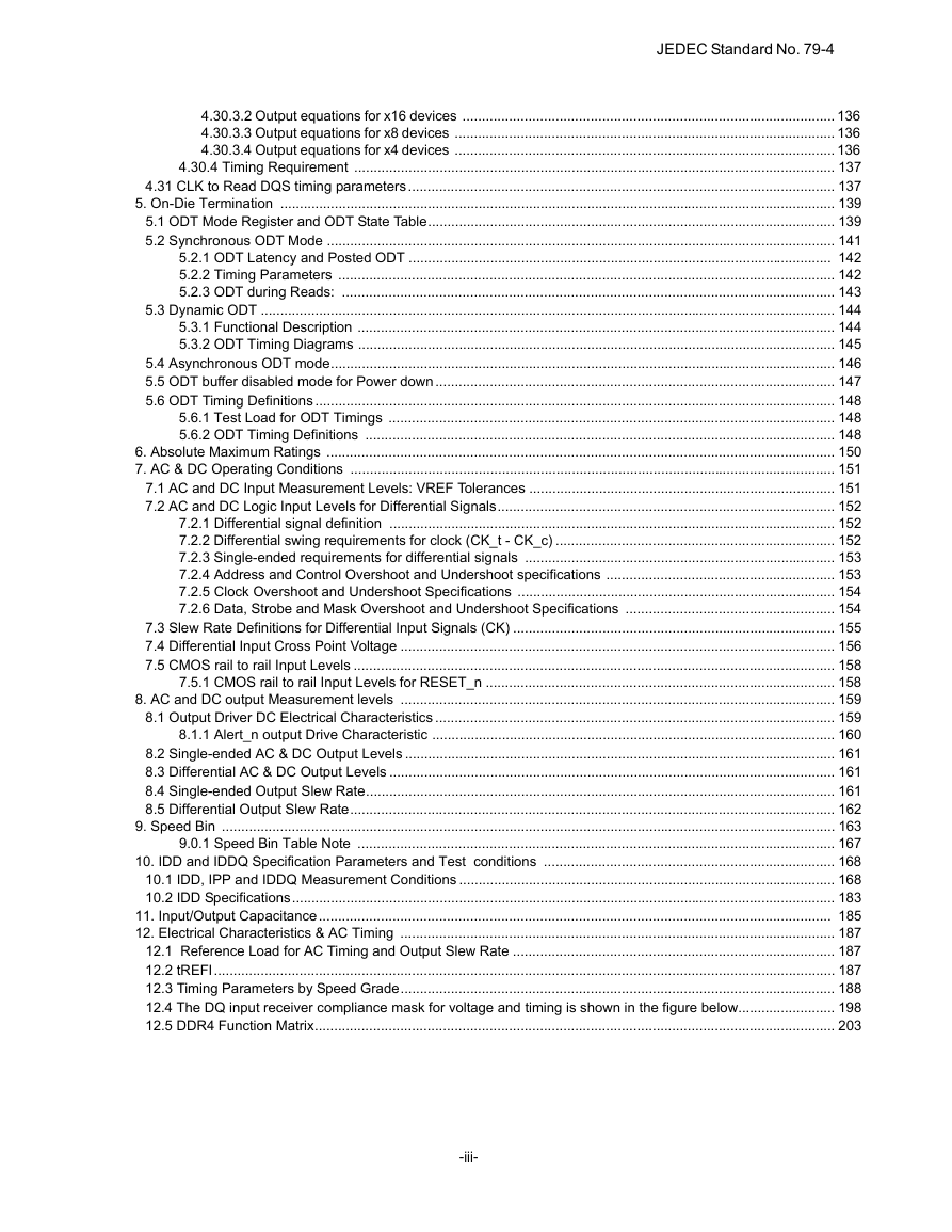
5 On-Die Termination
5.1 ODT Mode Register and ODT State Table
5.2 Synchronous ODT Mode
5.2.1 ODT Latency and Posted ODT
5.2.2 Timing Parameters
5.2.3 ODT during Reads:
5.3 Dynamic ODT
5.3.1 Functional Description
5.3.2 ODT Timing Diagrams
5.4 Asynchronous ODT mode
5.5 ODT buffer disabled mode for Power down
5.6 ODT Timing Definitions
5.6.1 Test Load for ODT Timings
5.6.2 ODT Timing Definitions
6 Absolute Maximum Ratings
7 AC & DC Operating Conditions
7.1 AC and DC Input Measurement Levels: VREF Tolerances
7.2 AC and DC Logic Input Levels for Differential Signals
7.2.1 Differential signal definition
7.2.2 Differential swing requirements for clock (CK_t - CK_c)
7.2.3 Single-ended requirements for differential signals
7.2.4 Address and Control Overshoot and Undershoot specifications
7.2.5 Clock Overshoot and Undershoot Specifications
7.2.6 Data, Strobe and Mask Overshoot and Undershoot Specifications
7.3 Slew Rate Definitions for Differential Input Signals (CK)
7.4 Differential Input Cross Point Voltage
7.5 CMOS rail to rail Input Levels
7.5.1 CMOS rail to rail Input Levels for RESET_n
8 AC and DC output Measurement levels
8.1 Output Driver DC Electrical Characteristics
8.1.1 Alert_n output Drive Characteristic
8.2 Single-ended AC & DC Output Levels
8.3 Differential AC & DC Output Levels
8.4 Single-ended Output Slew Rate
8.5 Differential Output Slew Rate
9 Speed Bin
9.1 Speed Bin Table Note
10 IDD and IDDQ Specification Parameters and Test conditions
10.1 IDD, IPP and IDDQ Measurement Conditions
10.2 IDD Specifications
11 Input/Output Capacitance
12 Electrical Characteristics & AC Timing
12.1 Reference Load for AC Timing and Output Slew Rate
12.2 tREFI
12.3 Timing Parameters by Speed Grade
12.4 The DQ input receiver compliance mask for voltage and timing (see figure)
12.5 DDR4 Function Matrix




 2023年江西萍乡中考道德与法治真题及答案.doc
 2012年重庆南川中考生物真题及答案.doc
 2013年江西师范大学地理学综合及文艺理论基础考研真题.doc
 2020年四川甘孜小升初语文真题及答案I卷.doc
 2020年注册岩土工程师专业基础考试真题及答案.doc
 2023-2024学年福建省厦门市九年级上学期数学月考试题及答案.doc
 2021-2022学年辽宁省沈阳市大东区九年级上学期语文期末试题及答案.doc
 2022-2023学年北京东城区初三第一学期物理期末试卷及答案.doc
 2018上半年江西教师资格初中地理学科知识与教学能力真题及答案.doc
 2012年河北国家公务员申论考试真题及答案-省级.doc
 2020-2021学年江苏省扬州市江都区邵樊片九年级上学期数学第一次质量检测试题及答案.doc
 2022下半年黑龙江教师资格证中学综合素质真题及答案.doc