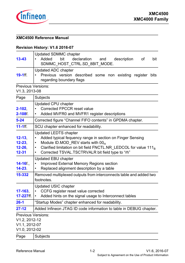
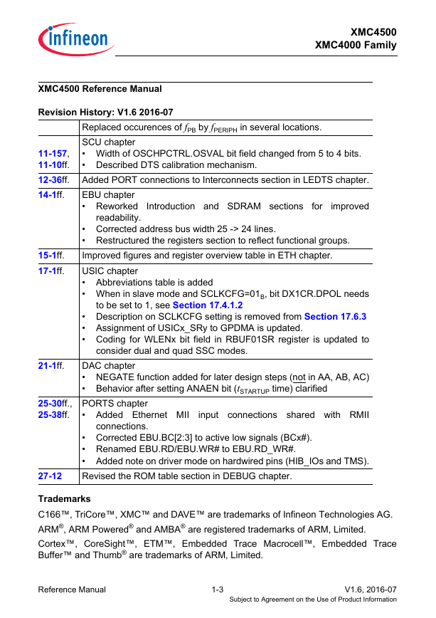
Revision History
About this Document
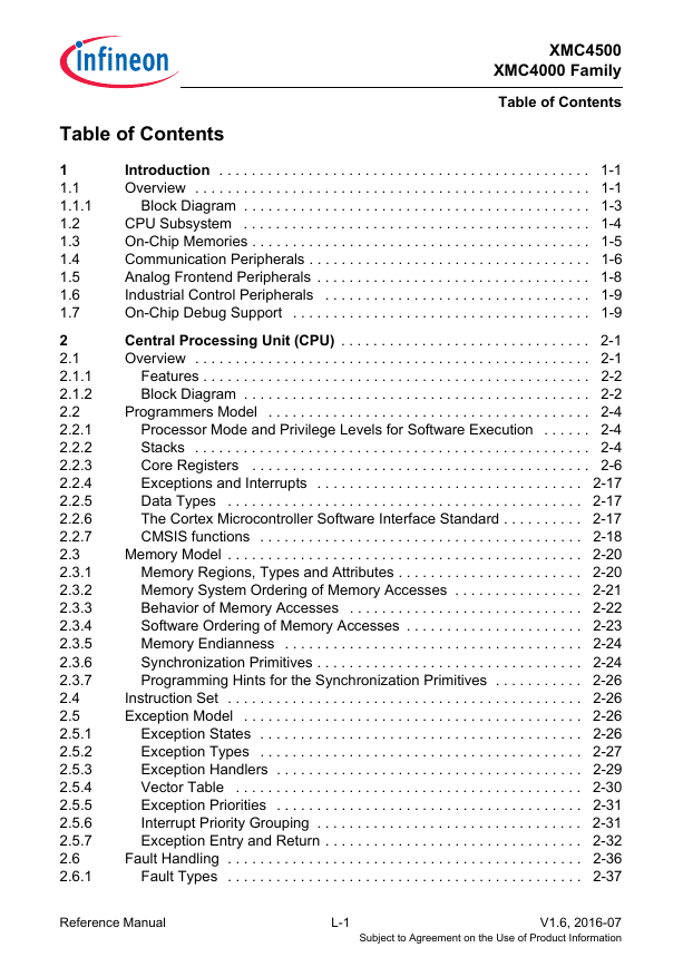
Introduction
1 Introduction
1.1 Overview
1.1.1 Block Diagram
1.2 CPU Subsystem
1.3 On-Chip Memories
1.4 Communication Peripherals
1.5 Analog Frontend Peripherals
1.6 Industrial Control Peripherals
1.7 On-Chip Debug Support
CPU Subsystem
2 Central Processing Unit (CPU)
2.1 Overview
2.1.1 Features
2.1.2 Block Diagram
2.2 Programmers Model
2.2.1 Processor Mode and Privilege Levels for Software Execution
2.2.2 Stacks
2.2.3 Core Registers
2.2.4 Exceptions and Interrupts
2.2.5 Data Types
2.2.6 The Cortex Microcontroller Software Interface Standard
2.2.7 CMSIS functions
2.3 Memory Model
2.3.1 Memory Regions, Types and Attributes
2.3.2 Memory System Ordering of Memory Accesses
2.3.3 Behavior of Memory Accesses
2.3.4 Software Ordering of Memory Accesses
2.3.5 Memory Endianness
2.3.6 Synchronization Primitives
2.3.7 Programming Hints for the Synchronization Primitives
2.4 Instruction Set
2.5 Exception Model
2.5.1 Exception States
2.5.2 Exception Types
2.5.3 Exception Handlers
2.5.4 Vector Table
2.5.5 Exception Priorities
2.5.6 Interrupt Priority Grouping
2.5.7 Exception Entry and Return
2.6 Fault Handling
2.6.1 Fault Types
2.6.2 Fault Escalation and Hard Faults
2.6.3 Fault Status Registers and Fault Address Registers
2.6.4 Lockup
2.7 Power Management
2.7.1 Entering Sleep Mode
2.7.2 Wakeup from Sleep Mode
2.7.3 The External Event Input
2.7.4 Power Management Programming Hints
2.8 Private Peripherals
2.8.1 About the Private Peripherals
2.8.2 System control block
2.8.2.1 System control block design hints and tips
2.8.3 System timer, SysTick
2.8.3.1 SysTick design hints and tips
2.8.4 Nested Vectored Interrupt Controller (NVIC)
2.8.4.1 Level-sensitive and pulse interrupts
2.8.4.2 NVIC design hints and tips
2.8.4.3 Using CMSIS functions to access NVIC
2.8.5 Memory Protection Unit (MPU)
2.8.5.1 MPU Access Permission Attributes
2.8.5.2 MPU Mismatch
2.8.5.3 Updating an MPU Region
2.8.5.4 MPU Design Hints and Tips
2.8.6 Floating Point Unit (FPU)
2.8.6.1 Enabling the FPU
2.9 PPB Registers
2.9.1 SCS Registers
2.9.2 SysTick Registers
2.9.3 NVIC Registers
2.9.4 MPU Registers
2.9.5 FPU Registers
3 Bus System
3.1 Bus Interfaces
3.2 Bus Matrix
4 Service Request Processing
4.1 Overview
4.1.1 Features
4.1.2 Block Diagram
4.2 Service Request Distribution
4.3 Interrupt Service Requests
4.4 DMA Line Router (DLR)
4.4.1 Functional Description
4.4.2 DMA Service Request Source Selection
4.6 Service Request Generation
4.7 Debug Behavior
4.8 Power, Reset and Clock
4.9 Initialization and System Dependencies
4.10 Registers
4.10.1 DLR Registers
4.10.2 ERU Registers
4.11 Interconnects
4.11.1 ERU0 Connections
4.11.2 ERU1 Connections
5 General Purpose DMA (GPDMA)
5.1 Overview
5.1.1 Features
5.1.2 Block Diagram
5.2 Functional Description
5.2.1 Terminology
5.2.2 Variable Definitions
5.2.3 Flow Controller and Transfer Type
5.2.4 Handshaking Interface
5.2.4.1 Hardware Handshaking
5.2.4.2 Software Handshaking
5.2.4.3 Handshaking with GPDMA as Flow Controller
5.2.4.4 Handshaking with Peripheral as Flow Controller
5.2.5 FIFO Usage
5.2.6 Bus and Channel Locking
5.2.7 Scatter/Gather
5.2.8 Abnormal Transfer Termination
5.3 Basic Transfers
5.3.1 Block transfer with GPDMA as the flow controller
5.3.2 Effect of maximum AMBA burst length on a block transfer
5.4 Multi Block Transfers
5.4.1 Block Chaining Using Linked Lists
5.4.2 Auto-Reloading of Channel Registers
5.4.3 Contiguous Address Between Blocks
5.4.4 Suspension of Transfers Between Blocks
5.4.5 Ending Multi-Block Transfers
5.4.6 Programing Examples
5.4.6.1 Single-block Transfer
5.4.6.2 Multi-Block Transfer with Source Address Auto-Reloaded and Contiguous Destination Address
5.4.6.3 Multi-Block Transfer with Source and Destination Address Auto-Reloaded
5.4.6.4 Multi-Block Transfer with Source Address Auto-Reloaded and Linked List Destination Address
5.4.6.5 Multi-Block DMA Transfer with Linked List for Source and Contiguous Destination Address
5.4.6.6 Multi-Block Transfer with Linked List for Source and Destination
5.5 Service Request Generation
5.6 Power, Reset and Clock
5.7 Initialization and System Dependencies
5.8 Registers
5.8.1 Configuration and Channel Enable Registers
5.8.2 Channel Registers
5.8.3 Interrupt Registers
5.8.4 Software Handshaking Registers
5.8.5 Miscellaneous GPDMA Registers
6 Flexible CRC Engine (FCE)
6.1 Overview
6.1.1 Features
6.1.2 Application Mapping
6.1.3 Block Diagram
6.2 Functional Description
6.2.1 Basic Operation
6.2.2 Automatic Signature Check
6.2.3 Register protection and monitoring methods
6.3 Service Request Generation
6.4 Debug Behavior
6.5 Power, Reset and Clock
6.6 Initialization and System Dependencies
6.7 Registers
6.7.1 System Registers description
6.7.2 CRC Kernel Control/Status Registers
6.8 Interconnects
6.9 Properties of CRC code
On-Chip Memories
7 Memory Organization
7.1 Overview
7.1.1 Features
7.1.2 Cortex-M4 Address Space
7.2 Memory Regions
7.3 Memory Map
7.4 Service Request Generation
7.5 Debug Behavior
7.6 Power, Reset and Clock
7.7 Initialization and System Dependencies
7.8 Registers
8 Flash and Program Memory Unit (PMU)
8.1 Overview
8.1.1 Block Diagram
8.2 Boot ROM (BROM)
8.2.1 BROM Addressing
8.3 Prefetch Unit
8.3.1 Overview
8.3.2 Operation
8.3.2.1 Instruction Buffer
8.3.2.2 Data Buffer
8.3.2.3 PMU Interface
8.4 Program Flash (PFLASH)
8.4.1 Overview
8.4.1.1 Features
8.4.2 Definition of Terms
8.4.3 Flash Structure
8.4.4 Flash Read Access
8.4.5 Flash Write and Erase Operations
8.4.6 Modes of Operation
8.4.7 Command Sequences
8.4.7.1 Command Sequence Definitions
8.4.7.2 Flash Page Programming Example
8.4.8 Flash Protection
8.4.8.1 Configuring Flash Protection in the UCB
8.4.8.2 Flash Read Protection
8.4.8.3 Flash Write and OTP Protection
8.4.8.4 System Wide Effects of Flash Protection
8.4.9 Data Integrity and Safety
8.4.9.1 Error-Correcting Code (ECC)
8.4.9.2 Margin Checks
8.5 Service Request Generation
8.5.1 Interrupt Control
8.5.2 Trap Control
8.5.3 Handling Errors During Operation
8.5.3.1 SQER “Sequence Error”
8.5.3.2 PFOPER “Operation Error”
8.5.3.3 PROER “Protection Error”
8.5.3.4 VER “Verification Error”
8.5.3.5 PFSBER/DFSBER “Single-Bit Error”
8.5.3.6 Handling Flash Errors During Startup
8.6 Power, Reset and Clock
8.6.1 Power Supply
8.6.2 Power Reduction
8.6.3 Reset Control
8.6.3.1 Resets During Flash Operation
8.6.4 Clock
8.7 Registers
8.7.1 PMU Registers
8.7.1.1 PMU ID Register
8.7.2 Prefetch Registers
8.7.2.1 Prefetch Configuration Register
8.7.3 Flash Registers
8.7.3.1 Flash Status Definition
8.7.3.2 Flash Configuration Control
8.7.3.3 Flash Identification Register
8.7.3.4 Margin Check Control Register
8.7.3.5 Protection Configuration Indication
System Control
9 Window Watchdog Timer (WDT)
9.1 Overview
9.1.1 Features
9.1.2 Block Diagram
9.2 Time-Out Mode
9.3 Pre-warning Mode
9.4 Bad Service Operation
9.5 Service Request Processing
9.6 Debug Behavior
9.7 Power, Reset and Clock
9.8 Initialization and Control Sequence
9.8.1 Initialization & Start of Operation
9.8.2 Reconfiguration & Restart of Operation
9.8.3 Software Stop & Resume Operation
9.8.4 Enter Sleep/Deep Sleep & Resume Operation
9.8.5 Prewarning Alarm Handling
9.9 Registers
9.9.1 Registers Description
9.10 Interconnects
10 Real Time Clock (RTC)
10.1 Overview
10.1.1 Features
10.1.2 Block Diagram
10.2 RTC Operation
10.3 Register Access Operations
10.4 Service Request Processing
10.4.1 Periodic Service Request
10.4.2 Timer Alarm Service Request
10.5 Wake-up From Hibernation Trigger
10.5.1 Periodic Wake-up Trigger Generation
10.5.2 Timer Alarm Wake-up Trigger Generation
10.6 Debug behavior
10.7 Power, Reset and Clock
10.8 Initialization and Control Sequence
10.8.1 Initialization & Start of Operation
10.8.2 Re-configuration & Re-start of Operation
10.8.3 Configure and Enable Periodic Event
10.8.4 Configure and Enable Timer Event
10.9 Registers
10.9.1 Registers Description
10.10 Interconnects
11 System Control Unit (SCU)
11.1 Overview
11.1.1 Features
11.1.2 Block Diagram
11.2 Miscellaneous Control Functions
11.2.1 Startup Software Support
11.2.2 Service Requests
11.2.2.1 Service Request Sources
11.2.3 Memory Parity Protection
11.2.3.1 Parity Error Handling
11.2.4 Trap Generation
11.2.4.1 Trap Sources
11.2.5 Die Temperature Measurement
11.2.5.1 Temperature Measurement
11.2.5.2 Offset Adjustment
11.2.5.3 Gain Adjustment
11.2.6 Retention Memory
11.2.7 Out of Range Comparator Control
11.3 Power Management
11.3.1 Functional Description
11.3.2 System States
11.3.3 Hibernate Domain Operating Modes
11.3.4 Embedded Voltage Regulator (EVR)
11.3.5 Power-on Reset
11.3.6 Supply Watchdog (SWD)
11.3.7 Power Validation
11.3.8 Supply Voltage Brown-out Detection
11.3.9 Hibernate Domain Power Management
11.3.10 Flash Power Control
11.4 Hibernate Control
11.4.1 Hibernate Mode
11.4.2 Hibernate Domain Pin Functions
11.4.3 System Level Integration
11.5 Reset Control
11.5.1 Supported Reset types
11.5.2 Peripheral Reset Control
11.5.3 Reset Status
11.6 Clock Control
11.6.1 Block Diagram
11.6.2 Clock Sources
11.6.3 Clock System Overview
11.6.3.1 Clock System Architecture
11.6.4 High Precision Oscillator Circuit (OSC_HP)
11.6.5 Backup Clock Source
11.6.6 Main PLL
11.6.6.1 Features
11.6.6.2 System PLL Functional Description
11.6.6.3 Configuration and Operation of the Prescaler Mode
11.6.6.4 Bypass Mode
11.6.6.5 System Oscillator Watchdog (OSC_WDG)
11.6.6.6 VCO Power Down Mode
11.6.6.7 PLL Power Down Mode
11.6.7 Internally Generated System Clock Calibration
11.6.7.1 Factory Calibration
11.6.7.2 Automatic Calibration
11.6.7.3 Alternative Internal Clock Calibration
11.6.8 USB PLL
11.6.9 Ultra Low Power Oscillator
11.6.9.1 OSC_ULP Oscillator Watchdog (ULPWDG)
11.6.10 Internal Slow Clock Source
11.6.11 Clock Gating Control
11.7 Debug Behavior
11.8 Power, Reset and Clock
11.9 Initialization and System Dependencies
11.9.1 Power-Up
11.9.2 Power-on Reset Release
11.9.3 System Reset Release
11.9.4 Clock System Setup
11.9.5 Configuration of Special System Functions
11.9.6 Configuration of Miscellaneous Functions
11.10 Registers
11.10.1 GCU Registers
11.10.2 PCU Registers
11.10.3 HCU Registers
11.10.4 RCU Registers
11.10.5 CCU Registers
Communication Peripherals
12 LED and Touch-Sense (LEDTS)
12.1 Overview
12.1.1 Features
12.1.2 Block Diagram
12.2 Functional Overview
12.3 LED Drive Mode
12.3.1 LED Pin Assignment and Current Capability
12.4 Touch-Sense Mode
12.4.1 Finger Sensing
12.5 Operating both LED Drive and Touch-Sense Modes
12.6 Service Request Processing
12.7 Debug Behavior
12.8 Power, Reset and Clock
12.9 Initialisation and System Dependencies
12.9.1 Function Enabling
12.9.2 Interpretation of Bit Field FNCOL
12.9.3 LEDTS Timing Calculations
12.9.4 Time-Multiplexed LED and Touch-Sense Functions on Pin
12.9.5 LEDTS Pin Control
12.9.6 Software Hints
12.9.7 Hardware Design Hints
12.10 Registers
12.10.1 Registers Description
12.11 Interconnects
13 SD/MMC Interface (SDMMC)
13.1 Overview
13.1.1 Features
13.1.2 Block Diagram
13.2 Functional Description
13.3 Card Detection
13.4 Data Transfer Modes
13.5 Read/ Write Operation
13.5.1 Write Operation
13.5.2 Read Operation
13.5.3 Abort Transaction
13.6 Special Command Types
13.7 Error Detection
13.8 Service Request Generation
13.9 Debug Behavior
13.10 Power, Reset and Clocks
13.11 Initialisation and System Dependencies
13.11.1 Setup SDMMC Data Transfer
13.11.2 Read Operation
13.11.3 Write Operation
13.11.4 Abort Transaction
13.12 Registers
13.12.1 Registers Description
13.13 Interconnects
14 External Bus Unit (EBU)
14.1 Overview
14.1.1 Features
14.1.2 Block Diagram
14.2 Interface Signals
14.2.1 Allocation of Unused Signals as GPIO
14.2.2 Signal States when EBU is inactive
14.3 Memory Controller Structure
14.4 Memory Controller AHBIF Bridge
14.4.1 AHB Error Generation
14.4.2 Read Data Buffering
14.4.3 Write Data Buffering
14.5 Clocking Strategy and Local Clock Generation
14.5.1 Clocking Modes
14.5.1.1 Clock Requirements
14.5.2 Standby Mode
14.6 External Bus Operation
14.6.1 External Memory Regions
14.6.2 Chip Select Control
14.6.3 Programmable Device Types
14.6.4 Support for Multiplexed Device Configurations
14.6.5 Support for Non-Multiplexed Device Configurations
14.6.6 AHB Bus Width Translation
14.6.7 Address Alignment During Bus Accesses
14.7 External Bus Arbitration
14.7.1 External Bus Modes
14.7.2 Arbitration Signals and Parameters
14.7.3 Arbitration Modes
14.7.3.1 No Bus Mode
14.7.3.2 Sole Master Mode
14.7.3.3 Arbiter Mode
14.7.3.4 Participant Mode
14.7.4 Arbitration Input Signal Sampling
14.7.5 Locking the External Bus
14.7.6 Reaction to an AHB Access to the External Bus
14.7.7 Pending Access Time-Out
14.7.8 Arbitrating SDRAM control signals
14.8 Start-Up/Boot Process
14.9 Standard Access Phases
14.9.1 Address Phase (AP)
14.9.2 Address Hold Phase (AH)
14.9.3 Command Delay Phase (CD)
14.9.4 Command Phase (CP)
14.9.5 Data Hold Phase (DH)
14.9.6 Burst Phase (BP)
14.9.7 Recovery Phase (RP)
14.10 Asynchronous Read/Write Accesses
14.10.1 Signal List
14.10.2 Standard Asynchronous Access Phases
14.10.3 Control of ADV & CS Delays During Asynchronous Accesses
14.10.4 Programmable Parameters
14.10.5 Accesses to Multiplexed Devices
14.10.6 Dynamic Command Delay and Wait State Insertion
14.10.6.1 External Extension of the Command Phase by WAIT
14.10.7 Interfacing to Nand Flash Devices
14.10.7.1 NAND flash page mode
14.11 Synchronous Read/Write Accesses
14.11.1 Signals
14.11.2 Support for four Burst FLASH device types
14.11.3 Typical Burst Flash Connection
14.11.4 Burst Flash Clock
14.11.5 Standard Access Phases
14.11.6 Burst Length Control
14.11.7 Control of ADV & CS Delays During Burst FLASH Access
14.11.8 Burst Flash Clock Feedback
14.11.9 Asynchronous Address Phase
14.11.10 Page Mode Support
14.11.11 Critical Word First Read Accesses
14.11.12 Example Burst Flash Access Cycle
14.11.13 External Cycle Control via the WAIT Input
14.11.14 Flash Non-Array Access Support
14.11.15 Termination of a Burst Access
14.11.16 Burst Flash Device Programming Sequences
14.11.17 Cellular RAM
14.11.18 Programmable Parameters
14.12 SDRAM Interface
14.12.1 Features
14.12.2 Signal List
14.12.3 External Interface
14.12.4 External Bus Clock Generation
14.12.5 SDRAM Characteristics
14.12.6 Supported SDRAM commands
14.12.7 SDRAM device size
14.12.8 Power Up Sequence
14.12.9 Initialization sequence
14.12.10 Mobile SDRAM Support
14.12.11 Burst Accesses
14.12.12 Short Burst Accesses
14.12.13 Multibanking Operation
14.12.14 Bank Mask
14.12.15 Row Mask
14.12.16 Banks Precharge
14.12.17 Refresh Cycles
14.12.18 Self-Refresh Mode
14.12.19 SDRAM Addressing Scheme
14.12.20 Power Down Mode
14.12.21 SDRAM Recovery Phases
14.12.22 Programmable Parameters
14.13 Debug Behavior
14.14 Power, Reset and Clock
14.14.1 Clocks
14.14.2 Module Reset
14.14.3 Power
14.15 System Dependencies
14.16 Registers
14.16.1 General Control Registers
14.16.2 Region Control Registers
14.16.3 SDRAM Control Registers
15 Ethernet MAC (ETH)
15.1 Overview
15.1.1 ETH Core Features
15.1.2 DMA Block Features
15.1.3 Transaction Layer (MTL) Features
15.1.4 Monitoring, Test, and Debugging Support Features
15.1.5 Block Diagram
15.2 Functional Description
15.2.1 ETH Core
15.2.1.1 Transmission
15.2.1.2 MAC Transmit Interface Protocol
15.2.1.3 Reception
15.2.2 MAC Transaction Layer (MTL)
15.2.2.1 Transmit Path
15.2.2.2 Receive Path
15.2.3 DMA Controller
15.2.3.1 Initialization
15.2.3.2 Transmission
15.2.3.3 Reception
15.2.3.4 Interrupts
15.2.4 DMA Descriptors
15.2.4.1 Descriptor Formats
15.2.5 MAC Management Counters
15.2.6 Power Management Block
15.2.6.1 PMT Block Description
15.2.6.2 Remote Wake-Up Frame Detection
15.2.6.3 Magic Packet Detection
15.2.6.4 System Considerations During Power-Down
15.2.7 PHY Interconnect
15.2.7.1 PHY Interconnect selection
15.2.8 Station Management Interface
15.2.8.1 Station Management Functions
15.2.8.2 Station Management Write Operation
15.2.8.3 Station Management Read Operation
15.2.9 Media Independent interface
15.2.10 Reduced Media Independent Interface
15.2.10.1 RMII Block Diagram
15.2.10.2 RMII Block Overview
15.2.10.3 Transmit Bit Ordering
15.2.10.4 RMII Transmit Timing Diagrams
15.2.11 IEEE 1588-2002 Overview
15.2.11.1 Reference Timing Source
15.2.11.2 Transmit Path Functions
15.2.11.3 Receive Path Functions
15.2.11.4 Time Stamp Error Margin
15.2.11.5 Frequency Range of Reference Timing Clock
15.2.11.6 Advanced Time Stamp Feature Support
15.2.11.7 Peer-to-Peer PTP (Pdelay) Transparent Clock (P2P TC) Message Support
15.2.11.8 Clock Types
15.2.11.9 PTP Processing and Control
15.2.11.10 Reference Timing Source (for Advance Timestamp Feature)
15.2.11.11 Transmit Path Functions
15.2.11.12 Receive Path Functions
15.2.12 System Time Register Module
15.2.13 Application BUS Interface
15.3 Service Request Generation
15.3.1 DMA Service Requests
15.3.2 Power Management Service Requests
15.3.3 System Time Module
15.3.4 MAC Management Counter Service Requests
15.4 Debug
15.5 Power Reset and Clock
15.6 ETH Registers
15.6.1 Register Description
15.6.2 Registers Overview
15.6.2.1 Registers Description
15.7 Interconnects
15.7.1 ETH Pins
16 Universal Serial Bus (USB)
16.1 Overview
16.1.1 Features
16.1.2 Block Diagram
16.2 Functional Description
16.2.1 OTG Dual-Role Device (DRD)
16.2.2 USB Host
16.2.3 USB Device
16.2.4 FIFO Architecture
16.2.4.1 Host FIFO Architecture
16.2.4.2 Device FIFO Architecture
16.3 Programming Overview
16.3.1 Programming Options on DMA
16.3.1.1 DMA Mode
16.3.1.2 Slave Mode
16.3.2 Core Initialization
16.4 Host Programming Overview
16.4.1 Host Initialization
16.4.2 Host Connection
16.4.3 Host Disconnection
16.4.4 Channel Initialization in Buffer DMA or Slave Mode
16.4.5 Halting a Channel
16.4.6 Selecting the Queue Depth
16.4.7 Handling Special Conditions
16.4.7.1 Handling Babble Conditions
16.4.7.2 Handling Disconnects
16.4.8 Host HFIR Functionality
16.4.8.1 HFIR Behaviour when HFIR.HFIRRldCtrl = 0B
16.4.8.2 HFIR Behaviour when HFIR.HFIRRldCtrl = 1B
16.4.9 Host Programming for Various USB Transactions
16.5 Host Programming in Slave mode
16.5.1 Writing the Transmit FIFO in Slave Mode
16.5.2 Reading the Receive FIFO in Slave Mode
16.5.3 Control Transactions in Slave Mode
16.5.4 Bulk and Control IN Transactions in Slave Mode
16.5.4.1 Normal Bulk and Control IN Operations
16.5.4.2 Handling Interrupts
16.5.5 Bulk and Control OUT/SETUP Transactions in Slave Mode
16.5.5.1 Normal Bulk and Control OUT/SETUP Operations
16.5.5.2 Handling Interrupts
16.5.6 Interrupt IN Transactions in Slave Mode
16.5.6.1 Normal Interrupt IN Operation
16.5.6.2 Handling Interrupts
16.5.7 Interrupt OUT Transactions in Slave Mode
16.5.7.1 Normal Interrupt OUT Operation
16.5.7.2 Handling Interrupts
16.5.8 Isochronous IN Transactions in Slave Mode
16.5.8.1 Normal Isochronous IN Operation
16.5.8.2 Handling Interrupts
16.5.9 Isochronous OUT Transactions in Slave Mode
16.5.9.1 Normal Isochronous OUT Operation
16.5.9.2 Handling Interrupts
16.6 Host Programming in Buffer DMA Mode
16.6.1 Control Transactions in Buffer DMA Mode
16.6.2 Bulk and Control IN Transactions in Buffer DMA Mode
16.6.2.1 Normal Bulk and Control IN Operations
16.6.2.2 Handling Interrupts
16.6.3 Bulk and Control OUT/SETUP Transactions in Buffer DMA Mode
16.6.3.1 Overview
16.6.3.2 Normal Bulk and Control OUT/SETUP Operations
16.6.3.3 NAK and NYET Handling With Internal DMA
16.6.3.4 Handling Interrupts
16.6.4 Interrupt IN Transactions in Buffer DMA Mode
16.6.4.1 Normal Interrupt IN Operation
16.6.4.2 Handling Interrupts
16.6.5 Interrupt OUT Transactions in Buffer DMA Mode
16.6.5.1 Normal Interrupt OUT Operation
16.6.5.2 Handling Interrupts
16.6.6 Isochronous IN Transactions in Buffer DMA Mode
16.6.6.1 Normal Isochronous IN Operation
16.6.6.2 Handling Interrupts
16.6.7 Isochronous OUT Transactions in Buffer DMA Mode
16.6.7.1 Normal Isochronous OUT Operation
16.6.7.2 Handling Interrupts
16.7 Host Programming in Scatter-Gather DMA Mode
16.7.1 Programming Requirements
16.7.2 SPRAM Requirements
16.7.2.1 Descriptor Memory Structures
16.7.2.2 IN Memory Structure
16.7.2.3 OUT Memory Structure
16.7.3 Channel Initialization in Scatter-Gather DMA Mode
16.7.4 Asynchronous Transfers
16.7.4.1 Asynchronous Transfer Descriptor
16.7.5 Periodic Transfers
16.7.5.1 Isochronous Transactions
16.7.5.2 Interrupt Transactions
16.8 Device Programming Overview
16.8.1 Device Initialization
16.8.2 Device Connection
16.8.3 Device Disconnection
16.8.3.1 Device Soft Disconnection
16.8.4 Endpoint Initialization
16.8.4.1 Initialization on USB Reset
16.8.4.2 Initialization on Enumeration Completion
16.8.4.3 Initialization on SetAddress Command
16.8.4.4 Initialization on SetConfiguration/SetInterface Command
16.8.4.5 Endpoint Activation
16.8.4.6 Endpoint Deactivation
16.8.5 Programming OUT Endpoint Features
16.8.5.1 Disabling an OUT Endpoint
16.8.5.2 Stalling a Non-Isochronous OUT Endpoint
16.8.5.3 Setting the Global OUT NAK
16.8.5.4 Transfer Stop Programming for OUT Endpoints
16.8.6 Programming IN Endpoint Features
16.8.6.1 Setting IN Endpoint NAK
16.8.6.2 IN Endpoint Disable
16.8.6.3 Timeout for Control IN Endpoints
16.8.6.4 Stalling Non-Isochronous IN Endpoints
16.8.6.5 Transfer Stop Programming for IN Endpoints
16.8.6.6 Non-Periodic IN Endpoint Sequencing
16.8.7 Worst-Case Response Time
16.8.8 Choosing the Value of GUSBCFG.USBTrdTim
16.8.9 Handling Babble Conditions
16.8.10 Device Programming Operations in Buffer DMA or Slave Mode
16.9 Device Programming in Slave Mode
16.9.1 Control Transfers
16.9.1.1 Control Write Transfers (SETUP, Data OUT, Status IN)
16.9.1.2 Control Read Transfers (SETUP, Data IN, Status OUT)
16.9.1.3 Two-Stage Control Transfers (SETUP/Status IN)
16.9.1.4 Packet Read from FIFO
16.9.2 IN Data Transfers
16.9.2.1 Packet Write
16.9.3 OUT Data Transfers
16.9.3.1 Control Setup Transactions
16.9.3.2 Handling More Than Three Back-to-Back SETUP Packets
16.9.4 Non-Periodic (Bulk and Control) IN Data Transfers
16.9.4.1 Examples
16.9.5 Non-Isochronous OUT Data Transfers
16.9.6 Isochronous OUT Data Transfers
16.9.7 Isochronous OUT Data Transfers Using Periodic Transfer Interrupt
16.9.8 Incomplete Isochronous OUT Data Transfers
16.9.9 Incomplete Isochronous IN Data Transfers
16.9.10 Periodic IN (Interrupt and Isochronous) Data Transfers
16.9.11 Periodic IN Data Transfers Using the Periodic Transfer Interrupt
16.9.12 Interrupt OUT Data Transfers Using Periodic Transfer Interrupt
16.10 Device Programming in Buffer DMA Mode
16.10.1 Control Transfers
16.10.1.1 Control Write Transfers (SETUP, Data OUT, Status IN)
16.10.1.2 Control Read Transfers (SETUP, Data IN, Status OUT)
16.10.1.3 Two-Stage Control Transfers (SETUP/Status IN)
16.10.2 OUT Data Transfers
16.10.2.1 Control Setup Transactions
16.10.3 Non-Periodic (Bulk and Control) IN Data Transfers
16.10.4 Non-Isochronous OUT Data Transfers
16.10.5 Incomplete Isochronous OUT Data Transfers
16.10.6 Periodic IN (Interrupt and Isochronous) Data Transfers
16.10.7 Periodic IN Data Transfers Using the Periodic Transfer Interrupt
16.10.8 Interrupt OUT Data Transfers Using Periodic Transfer Interrupt
16.11 Device Programming in Scatter-Gather DMA Mode
16.11.1 Programming Overview
16.11.2 SPRAM Requirements
16.11.3 Descriptor Memory Structures
16.11.3.1 OUT Data Memory Structure
16.11.3.2 Isochronous OUT
16.11.3.3 Non-Isochronous OUT
16.11.3.4 IN Data Memory Structure
16.11.3.5 Descriptor Update Interrupt Enable Modes
16.11.3.6 DMA Arbitration in Scatter/Gather DMA Mode
16.11.3.7 Buffer Data Access on AHB in Scatter/Gather DMA Mode
16.11.4 Control Transfer Handling
16.11.5 Interrupt Usage for Control Transfers
16.11.6 Application Programming Sequence
16.11.7 Internal Data Flow
16.11.7.1 Three-Stage Control Write
16.11.7.2 Three-Stage Control Read
16.11.7.3 Two-Stage Control Transfer
16.11.7.4 Back to Back SETUP During Control Write
16.11.7.5 Back-to-Back SETUPs During Control Read
16.11.7.6 Extra Tokens During Control Write Data Phase
16.11.7.7 Extra Tokens During Control Read Data Phase
16.11.7.8 Premature SETUP During Control Write Data Phase
16.11.7.9 Premature SETUP During Control Read Data Phase
16.11.7.10 Premature Status During Control Write
16.11.7.11 Premature Status During Control Read
16.11.7.12 Lost ACK During Last Packet of Control Read
16.11.8 Bulk Transfer Handling in Scatter/Gather DMA Mode
16.11.8.1 Bulk IN Transfer in Scatter-Gather DMA Mode
16.11.8.2 Bulk OUT Transfer in Scatter-Gather DMA Mode
16.11.9 Interrupt Transfer Handling in Scatter/Gather DMA Mode
16.11.9.1 Interrupt IN Transfer in Scatter/Gather DMA Mode
16.11.9.2 Interrupt OUT Transfer in Scatter/Gather DMA Mode
16.11.10 Isochronous Transfer Handling in Scatter/Gather DMA Mode
16.11.10.1 Isochronous IN Transfer in Scatter/Gather DMA Mode
16.11.10.2 Isochronous OUT Transfer in Scatter/Gather DMA Mode
16.12 OTG Revision 1.3 Programming Model
16.12.1 A-Device Session Request Protocol
16.12.2 B-Device Session Request Protocol
16.12.3 A-Device Host Negotiation Protocol
16.12.4 B-Device Host Negotiation Protocol
16.13 Clock Gating Programming Model
16.13.1 Host Mode Suspend and Resume With Clock Gating
16.13.2 Host Mode Suspend and Remote Wakeup With Clock Gating
16.13.3 Host Mode Session End and Start With Clock Gating
16.13.4 Host Mode Session End and SRP With Clock Gating
16.13.5 Device Mode Suspend and Resume With Clock Gating
16.13.6 Device Mode Suspend and Remote Wakeup With Clock Gating
16.13.7 Device Mode Session End and Start With Clock Gating
16.13.8 Device Mode Session End and SRP With Clock Gating
16.14 FIFO RAM Allocation
16.14.1 Data FIFO RAM Allocation
16.14.1.1 Device Mode RAM Allocation
16.14.1.2 Host Mode RAM Allocation
16.14.2 Dynamic FIFO Allocation
16.14.2.1 Dynamic FIFO Reallocation in Host Mode
16.14.2.2 Dynamic FIFO Reallocation in Device Mode
16.14.2.3 Flushing TxFIFOs in the Core
16.15 Service Request Generation
16.16 Debug Behaviour
16.17 Power, Reset and Clock
16.18 Initialization and System Dependencies
16.19 Registers
16.19.1 Register Description
16.20 Interconnects
17 Universal Serial Interface Channel (USIC)
17.1 Overview
17.1.1 Features
17.2 Operating the USIC
17.2.1 USIC Structure Overview
17.2.1.1 Channel Structure
17.2.1.2 Input Stages
17.2.1.3 Output Signals
17.2.1.4 Baud Rate Generator
17.2.1.5 Channel Events and Interrupts
17.2.1.6 Data Shifting and Handling
17.2.2 Operating the USIC Communication Channel
17.2.2.1 Protocol Control and Status
17.2.2.2 Mode Control
17.2.2.3 General Channel Events and Interrupts
17.2.2.4 Data Transfer Events and Interrupts
17.2.2.5 Baud Rate Generator Event and Interrupt
17.2.2.6 Protocol-specific Events and Interrupts
17.2.3 Operating the Input Stages
17.2.3.1 General Input Structure
17.2.3.2 Digital Filter
17.2.3.3 Edge Detection
17.2.3.4 Selected Input Monitoring
17.2.3.5 Loop Back Mode
17.2.4 Operating the Baud Rate Generator
17.2.4.1 Fractional Divider
17.2.4.2 External Frequency Input
17.2.4.3 Divider Mode Counter
17.2.4.4 Capture Mode Timer
17.2.4.5 Time Quanta Counter
17.2.4.6 Master and Shift Clock Output Configuration
17.2.5 Operating the Transmit Data Path
17.2.5.1 Transmit Buffering
17.2.5.2 Transmit Data Shift Mode
17.2.5.3 Transmit Control Information
17.2.5.4 Transmit Data Validation
17.2.6 Operating the Receive Data Path
17.2.6.1 Receive Buffering
17.2.6.2 Receive Data Shift Mode
17.2.6.3 Baud Rate Constraints
17.2.7 Hardware Port Control
17.2.8 Operating the FIFO Data Buffer
17.2.8.1 FIFO Buffer Partitioning
17.2.8.2 Transmit Buffer Events and Interrupts
17.2.8.3 Receive Buffer Events and Interrupts
17.2.8.4 FIFO Buffer Bypass
17.2.8.5 FIFO Access Constraints
17.2.8.6 Handling of FIFO Transmit Control Information
17.3 Asynchronous Serial Channel (ASC = UART)
17.3.1 Signal Description
17.3.2 Frame Format
17.3.2.1 Idle Time
17.3.2.2 Start Bit Detection
17.3.2.3 Data Field
17.3.2.4 Parity Bit
17.3.2.5 Stop Bit(s)
17.3.3 Operating the ASC
17.3.3.1 Bit Timing
17.3.3.2 Baud Rate Generation
17.3.3.3 Noise Detection
17.3.3.4 Collision Detection
17.3.3.5 Pulse Shaping
17.3.3.6 Automatic Shadow Mechanism
17.3.3.7 End of Frame Control
17.3.3.8 Mode Control Behavior
17.3.3.9 Disabling ASC Mode
17.3.3.10 Protocol Interrupt Events
17.3.3.11 Data Transfer Interrupt Handling
17.3.3.12 Baud Rate Generator Interrupt Handling
17.3.3.13 Protocol-Related Argument and Error
17.3.3.14 Receive Buffer Handling
17.3.3.15 Sync-Break Detection
17.3.3.16 Transfer Status Indication
17.3.4 ASC Protocol Registers
17.3.4.1 ASC Protocol Control Register
17.3.4.2 ASC Protocol Status Register
17.3.5 Hardware LIN Support
17.4 Synchronous Serial Channel (SSC)
17.4.1 Signal Description
17.4.1.1 Transmit and Receive Data Signals
17.4.1.2 Shift Clock Signals
17.4.1.3 Slave Select Signals
17.4.2 Operating the SSC
17.4.2.1 Automatic Shadow Mechanism
17.4.2.2 Mode Control Behavior
17.4.2.3 Disabling SSC Mode
17.4.2.4 Data Frame Control
17.4.2.5 Parity Mode
17.4.2.6 Transfer Mode
17.4.2.7 Data Transfer Interrupt Handling
17.4.2.8 Baud Rate Generator Interrupt Handling
17.4.2.9 Protocol-Related Argument and Error
17.4.2.10 Receive Buffer Handling
17.4.2.11 Multi-IO SSC Protocols
17.4.3 Operating the SSC in Master Mode
17.4.3.1 Baud Rate Generation
17.4.3.2 MSLS Generation
17.4.3.3 Automatic Slave Select Update
17.4.3.4 Slave Select Delay Generation
17.4.3.5 Protocol Interrupt Events
17.4.3.6 End-of-Frame Control
17.4.4 Operating the SSC in Slave Mode
17.4.4.1 Protocol Interrupts
17.4.4.2 End-of-Frame Control
17.4.5 SSC Protocol Registers
17.4.5.1 SSC Protocol Control Registers
17.4.5.2 SSC Protocol Status Register
17.4.6 SSC Timing Considerations
17.4.6.1 Closed-loop Delay
17.4.6.2 Delay Compensation in Master Mode
17.4.6.3 Complete Closed-loop Delay Compensation
17.5 Inter-IC Bus Protocol (IIC)
17.5.1 Introduction
17.5.1.1 Signal Description
17.5.1.2 Symbols
17.5.1.3 Frame Format
17.5.2 Operating the IIC
17.5.2.1 Transmission Chain
17.5.2.2 Byte Stretching
17.5.2.3 Master Arbitration
17.5.2.4 Non-Acknowledge and Error Conditions
17.5.2.5 Mode Control Behavior
17.5.2.6 Data Transfer Interrupt Handling
17.5.2.7 IIC Protocol Interrupt Events
17.5.2.8 Baud Rate Generator Interrupt Handling
17.5.2.9 Receiver Address Acknowledge
17.5.2.10 Receiver Handling
17.5.2.11 Receiver Status Information
17.5.3 Symbol Timing
17.5.3.1 Start Symbol
17.5.3.2 Repeated Start Symbol
17.5.3.3 Stop Symbol
17.5.3.4 Data Bit Symbol
17.5.4 Data Flow Handling
17.5.4.1 Transmit Data Formats
17.5.4.2 Valid Master Transmit Data Formats
17.5.4.3 Master Transmit/Receive Modes
17.5.4.4 Slave Transmit/Receive Modes
17.5.5 IIC Protocol Registers
17.5.5.1 IIC Protocol Control Registers
17.5.5.2 IIC Protocol Status Register
17.6 Inter-IC Sound Bus Protocol (IIS)
17.6.1 Introduction
17.6.1.1 Signal Description
17.6.1.2 Protocol Overview
17.6.1.3 Transfer Delay
17.6.1.4 Connection of External Audio Components
17.6.2 Operating the IIS
17.6.2.1 Frame Length and Word Length Configuration
17.6.2.2 Automatic Shadow Mechanism
17.6.2.3 Mode Control Behavior
17.6.2.4 Transfer Delay
17.6.2.5 Parity Mode
17.6.2.6 Transfer Mode
17.6.2.7 Data Transfer Interrupt Handling
17.6.2.8 Baud Rate Generator Interrupt Handling
17.6.2.9 Protocol-Related Argument and Error
17.6.2.10 Transmit Data Handling
17.6.2.11 Receive Buffer Handling
17.6.2.12 Loop-Delay Compensation
17.6.3 Operating the IIS in Master Mode
17.6.3.1 Baud Rate Generation
17.6.3.2 WA Generation
17.6.3.3 Master Clock Output
17.6.3.4 Protocol Interrupt Events
17.6.4 Operating the IIS in Slave Mode
17.6.4.1 Protocol Events and Interrupts
17.6.5 IIS Protocol Registers
17.6.5.1 IIS Protocol Control Registers
17.6.5.2 IIS Protocol Status Register
17.7 Service Request Generation
17.8 Debug Behaviour
17.9 Power, Reset and Clock
17.10 Initialization and System Dependencies
17.11 Registers
17.11.1 Address Map
17.11.2 Module Identification Registers
17.11.3 Channel Control and Configuration Registers
17.11.3.1 Channel Control Register
17.11.3.2 Channel Configuration Register
17.11.3.3 Kernel State Configuration Register
17.11.3.4 Interrupt Node Pointer Register
17.11.4 Protocol Related Registers
17.11.4.1 Protocol Control Registers
17.11.4.2 Protocol Status Register
17.11.4.3 Protocol Status Clear Register
17.11.5 Input Stage Register
17.11.5.1 Input Control Registers
17.11.6 Baud Rate Generator Registers
17.11.6.1 Fractional Divider Register
17.11.6.2 Baud Rate Generator Register
17.11.6.3 Capture Mode Timer Register
17.11.7 Transfer Control and Status Registers
17.11.7.1 Shift Control Register
17.11.7.2 Transmission Control and Status Register
17.11.7.3 Flag Modification Registers
17.11.8 Data Buffer Registers
17.11.8.1 Transmit Buffer Locations
17.11.8.2 Receive Buffer Registers RBUF0, RBUF1
17.11.8.3 Receive Buffer Registers RBUF, RBUFD, RBUFSR
17.11.9 FIFO Buffer and Bypass Registers
17.11.9.1 Bypass Registers
17.11.9.2 General FIFO Buffer Control Registers
17.11.9.3 Transmit FIFO Buffer Control Registers
17.11.9.4 Receive FIFO Buffer Control Registers
17.11.9.5 FIFO Buffer Data Registers
17.11.9.6 FIFO Buffer Pointer Registers
17.12 Interconnects
17.12.1 USIC Module 0 Interconnects
17.12.2 USIC Module 1 Interconnects
17.12.3 USIC Module 2 Interconnects
18 Controller Area Network Controller (MultiCAN)
18.1 Overview
18.1.1 Features
18.1.2 Block Diagram
18.2 CAN Basics
18.2.1 Addressing and Bus Arbitration
18.2.2 CAN Frame Formats
18.2.2.1 Data Frames
18.2.2.2 Remote Frames
18.2.2.3 Error Frames
18.2.3 The Nominal Bit Time
18.2.4 Error Detection and Error Handling
18.3 MultiCAN Kernel Functional Description
18.3.1 Module Structure
18.3.2 Port Input Control
18.3.3 CAN Node Control
18.3.3.1 Bit Timing Unit
18.3.3.2 Bitstream Processor
18.3.3.3 Error Handling Unit
18.3.3.4 CAN Frame Counter
18.3.3.5 CAN Node Interrupts
18.3.4 Message Object List Structure
18.3.4.1 Basics
18.3.4.2 List of Unallocated Elements
18.3.4.3 Connection to the CAN Nodes
18.3.4.4 List Command Panel
18.3.5 CAN Node Analysis Features
18.3.5.1 Analyzer Mode
18.3.5.2 Loop-Back Mode
18.3.5.3 Bit Timing Analysis
18.3.6 Message Acceptance Filtering
18.3.6.1 Receive Acceptance Filtering
18.3.6.2 Transmit Acceptance Filtering
18.3.7 Message Postprocessing
18.3.7.1 Message Object Interrupts
18.3.7.2 Pending Messages
18.3.8 Message Object Data Handling
18.3.8.1 Frame Reception
18.3.8.2 Frame Transmission
18.3.9 Message Object Functionality
18.3.9.1 Standard Message Object
18.3.9.2 Single Data Transfer Mode
18.3.9.3 Single Transmit Trial
18.3.9.4 Message Object FIFO Structure
18.3.9.5 Receive FIFO
18.3.9.6 Transmit FIFO
18.3.9.7 Gateway Mode
18.3.9.8 Foreign Remote Requests
18.4 Service Request Generation
18.5 Debug behavior
18.6 Power, Reset and Clock
18.6.1 Clock Control
18.6.2 Module Clock Generation
18.7 Register Description
18.7.1 Global Module Registers
18.7.2 CAN Node Registers
18.7.3 Message Object Registers
18.7.4 MultiCAN Module External Registers
18.8 Interconnects
18.8.1 Interfaces of the MultiCAN Module
18.8.2 Port and I/O Line Control
18.8.2.1 Input/Output Function Selection in Ports
18.8.2.2 MultiCAN Interrupt Output Connections
18.8.2.3 Connections to USIC Inputs
Analog Frontend Peripherals
19 Versatile Analog-to-Digital Converter (VADC)
19.1 Overview
19.2 Introduction and Basic Structure
19.3 Configuration of General Functions
19.3.1 General Clocking Scheme and Control
19.3.2 Priority Channel Assignment
19.4 Module Activation and Power Saving
19.5 Conversion Request Generation
19.5.1 Queued Request Source Handling
19.5.2 Channel Scan Request Source Handling
19.6 Request Source Arbitration
19.6.1 Arbiter Operation and Configuration
19.6.2 Conversion Start Mode
19.7 Analog Input Channel Configuration
19.7.1 Channel Parameters
19.7.2 Conversion Timing
19.7.3 Alias Feature
19.7.4 Conversion Modes
19.7.5 Compare with Standard Conversions (Limit Checking)
19.7.6 Utilizing Fast Compare Mode
19.7.7 Boundary Flag Control
19.8 Conversion Result Handling
19.8.1 Storage of Conversion Results
19.8.2 Data Alignment
19.8.3 Wait-for-Read Mode
19.8.4 Result FIFO Buffer
19.8.5 Result Event Generation
19.8.6 Data Modification
19.9 Synchronization of Conversions
19.9.1 Synchronized Conversions for Parallel Sampling
19.9.2 Equidistant Sampling
19.10 Safety Features
19.10.1 Broken Wire Detection
19.10.2 Signal Path Test Modes
19.10.3 Configuration of Test Functions
19.11 External Multiplexer Control
19.12 Service Request Generation
19.13 Registers
19.13.1 Module Identification
19.13.2 System Registers
19.13.3 General Registers
19.13.4 Arbitration and Source Registers
19.13.5 Channel Control Registers
19.13.6 Result Registers
19.13.7 Miscellaneous Registers
19.13.8 Service Request Registers
G0RESy
19.14 Interconnects
19.14.1 Product-Specific Configuration
19.14.2 Analog Module Connections in the XMC4500
19.14.3 Digital Module Connections in the XMC4500
20 Delta-Sigma Demodulator (DSD)
20.1 Overview
20.2 Introduction and Basic Structure
20.3 Configuration of General Functions
20.4 Input Channel Configuration
20.4.1 Modulator Clock Selection and Generation
20.4.2 Input Data Selection
20.4.3 External Modulator
20.4.4 Input Path Control
20.5 Main Filter Chain
20.5.1 CIC Filter
20.5.2 Integrator Stage
20.6 Auxiliary Filter
20.7 Conversion Result Handling
20.8 Service Request Generation
20.9 Resolver Support
20.9.1 Carrier Signal Generation
20.9.2 Return Signal Synchronization
20.10 Time-Stamp Support
20.11 Registers
20.11.1 Module Identification
20.11.2 System Registers
20.11.3 General Registers
20.11.4 Input Path Control
20.11.5 Filter Configuration
20.11.6 Conversion Result Handling
20.11.7 Service Request Registers
20.11.8 Miscellaneous Registers
20.12 Interconnects
20.12.1 Product-Specific Configuration
20.12.2 Digital Module Connections in the XMC4500
21 Digital to Analog Converter (DAC)
21.1 Overview
21.1.1 Features
21.1.2 Block Diagram
21.2 Operating Modes
21.2.1 Hardware features
21.2.1.1 Trigger Generators (TG)
21.2.1.2 Data FIFO buffer (FIFO)
21.2.1.3 Data output stage
21.2.1.4 Pattern Generators (PG) - Waveform Generator
21.2.1.5 Noise Generators (NG) - Pseudo Random Number Generator
21.2.1.6 Ramp Generators (RG)
21.2.2 Entering any Operating Mode
21.2.3 Single Value Mode
21.2.4 Data Processing Mode
21.2.4.1 FIFO Data Handling
21.2.5 Pattern Generation Mode
21.2.6 Noise Generation Mode
21.2.7 Ramp Generation Mode
21.3 Service Request Generation
21.4 Power, Reset and Clock
21.5 Initialization
21.6 Registers
21.6.1 Address Map
21.6.2 Register Overview
21.6.3 Register Description
21.6.3.1 DAC_ID Register
21.6.3.2 DAC Configuration Registers
21.6.3.3 DAC Data Registers
21.6.3.4 DAC Pattern Registers
21.7 Interconnects
21.7.1 Analog Connections
21.7.2 Digital Connections
21.7.2.1 Service Request Connections
21.7.2.2 Trigger Connections
21.7.2.3 Synchronization Interface of the Pattern Generator
Industrial Control Peripherals
22 Capture/Compare Unit 4 (CCU4)
22.1 Overview
22.1.1 Features
22.1.2 Block Diagram
22.2 Functional Description
22.2.1 CC4y Overview
22.2.2 Input Selector
22.2.3 Connection Matrix
22.2.4 Starting/Stopping the Timer
22.2.5 Counting Modes
22.2.5.1 Calculating the PWM Period and Duty Cycle
22.2.5.2 Updating the Period and Duty Cycle
22.2.5.3 Edge Aligned Mode
22.2.5.4 Center Aligned Mode
22.2.5.5 Single Shot Mode
22.2.6 Active/Passive Rules
22.2.7 External Events Control
22.2.7.1 External Start/Stop
22.2.7.2 External Counting Direction
22.2.7.3 External Gating Signal
22.2.7.4 External Count Signal
22.2.7.5 External Load
22.2.7.6 External Capture
22.2.7.7 External Modulation
22.2.7.8 TRAP Function
22.2.7.9 Status Bit Override
22.2.8 Multi-Channel Control
22.2.9 Timer Concatenation
22.2.10 PWM Dithering
22.2.11 Prescaler
22.2.11.1 Normal Prescaler Mode
22.2.11.2 Floating Prescaler Mode
22.2.12 CCU4 Usage
22.2.12.1 PWM Signal Generation
22.2.12.2 Prescaler Usage
22.2.12.3 PWM Dither
22.2.12.4 Capture Mode Usage
22.3 Service Request Generation
22.4 Debug Behavior
22.5 Power, Reset and Clock
22.5.1 Clocks
22.5.2 Module Reset
22.5.3 Power
22.6 Initialization and System Dependencies
22.6.1 Initialization Sequence
22.6.2 System Dependencies
22.7 Registers
22.7.1 Global Registers
22.7.2 Slice (CC4y) Registers
22.8 Interconnects
22.8.1 CCU40 Pins
22.8.2 CCU41 Pins
22.8.3 CCU42 pins
22.8.4 CCU43 pins
23 Capture/Compare Unit 8 (CCU8)
23.1 Overview
23.1.1 Features
23.1.2 Block Diagram
23.2 Functional Description
23.2.1 Overview
23.2.2 Input Selector
23.2.3 Connection Matrix
23.2.4 Start/Stop Control
23.2.5 Counting Modes
23.2.5.1 Calculating the PWM Period and Duty Cycle
23.2.5.2 Updating the Period and Duty Cycle
23.2.5.3 Edge Aligned Mode
23.2.5.4 Center Aligned Mode
23.2.5.5 Single Shot Mode
23.2.6 Active/Passive Rules
23.2.7 Compare Modes
23.2.7.1 Edge Aligned Compare Modes
23.2.7.2 Center Aligned Compare Modes
23.2.8 External Events Control
23.2.8.1 External Start/Stop
23.2.8.2 External Counting Direction
23.2.8.3 External Gating Signal
23.2.8.4 External Count Signal
23.2.8.5 External Load
23.2.8.6 External Capture
23.2.8.7 External Modulation
23.2.8.8 Trap Function
23.2.8.9 Status Bit Override
23.2.9 Multi-Channel Support
23.2.10 Timer Concatenation
23.2.11 Output Parity Checker
23.2.12 PWM Dithering
23.2.13 Prescaler
23.2.13.1 Normal Prescaler Mode
23.2.13.2 Floating Prescaler Mode
23.2.14 CCU8 Usage
23.2.14.1 PWM Signal Generation
23.2.14.2 Prescaler Usage
23.2.14.3 PWM Dither
23.2.14.4 Capture Mode Usage
23.2.14.5 Parity Checker Usage
23.3 Service Request Generation
23.4 Debug Behavior
23.5 Power, Reset and Clock
23.5.1 Clocks
23.5.2 Module Reset
23.5.3 Power
23.6 Initialization and System Dependencies
23.6.1 Initialization Sequence
23.6.2 System Dependencies
23.7 Registers
23.7.1 Global Registers
23.7.2 Slice (CC8y) Registers
23.8 Interconnects
23.8.1 CCU80 Pins
23.8.2 CCU81 Pins
24 Position Interface Unit (POSIF)
24.1 Overview
24.1.1 Features
24.1.2 Block Diagram
24.2 Functional Description
24.2.1 Overview
24.2.2 Function Selector
24.2.3 Hall Sensor Control
24.2.4 Quadrature Decoder Control
24.2.4.1 Quadrature Clock and Direction decoding
24.2.4.2 Index Control
24.2.5 Stand-Alone Multi-Channel Mode
24.2.6 Synchronous Start
24.2.7 Using the POSIF
24.2.7.1 Hall Sensor Mode Usage
24.2.7.2 Quadrature Decoder Mode usage
24.2.7.3 Stand-alone Multi-Channel Mode
24.3 Service Request Generation
24.3.1 Hall Sensor Mode flags
24.3.2 Quadrature Decoder Flags
24.4 Debug Behavior
24.5 Power, Reset and Clock
24.5.1 Clocks
24.5.2 Module Reset
24.5.3 Power
24.6 Initialization and System Dependencies
24.6.1 Initialization
24.6.2 System Dependencies
24.7 Registers
24.7.1 Global registers
24.7.2 Hall Sensor Mode Registers
24.7.3 Multi-Channel Mode Registers
24.7.4 Quadrature Decoder Registers
24.7.5 Interrupt Registers
24.8 Interconnects
24.8.1 POSIF0 Pins
24.8.2 POSIF1 Pins
General Purpose I/O Ports
25 General Purpose I/O Ports (PORTS)
25.1 Overview
25.1.1 Features
25.1.2 Block Diagram
25.1.3 Definition of Terms
25.2 GPIO and Alternate Function
25.2.1 Input Operation
25.2.2 Output Operation
25.3 Hardware Controlled I/Os
25.4 Power Saving Mode Operation
25.5 Analog Ports
25.6 Power, Reset and Clock
25.7 Initialization and System Dependencies
25.8 Registers
25.8.1 Port Input/Output Control Registers
25.8.2 Pad Driver Mode Register
25.8.3 Pin Function Decision Control Register
25.8.4 Port Output Register
25.8.5 Port Output Modification Register
25.8.6 Port Input Register
25.8.7 Port Pin Power Save Register
25.8.8 Port Pin Hardware Select Register
25.9 Package Pin Summary
25.10 Port I/O Functions
25.10.1 Port I/O Function Table
Startup Modes
26 Startup Modes
26.1 Overview
26.1.1 Features
26.2 Startup Modes
26.2.1 Reset Types and Corresponding Boot Modes
26.2.2 Initial Boot Sequence
26.2.3 Boot Mode Selection
26.2.4 Normal Boot Mode
26.2.5 Boot from PSRAM
26.2.6 Alternative Boot Mode - Address0 (ABM-0)
26.2.7 Alternative Boot Mode - Address1 (ABM-1)
26.2.8 Fallback ABM
26.2.9 ASC BSL Mode
26.2.10 CAN BSL Mode
26.2.11 Boot Mode Index (BMI)
26.3 Debug Behavior
26.3.1 Boot Modes and Hardware Debugger Support
26.3.2 Failures and Handling
26.4 Power, Reset and Clock
26.4.1 Clocking
26.4.2 Registers Modified by SSW
Debug and Trace System
27 Debug and Trace System (DBG)
27.1 Overview
27.2 Debug System Operation
27.2.1 Flash Patch Breakpoint (FPB)
27.2.2 Data Watchpoint and Trace (DWT)
27.2.3 Instrumentation Trace Macrocell (ITM)
27.2.4 Embedded Trace Macrocell (ETM)
27.2.5 Trace Port Interface Unit (TPIU)
27.3 Power, Reset and Clock
27.3.1 Reset
27.3.1.1 CoreSightTM resets
27.3.1.2 Serial Wire interface driven system reset
27.4 Initialization and System Dependencies
27.4.1 Debug accesses and Flash protection
27.4.2 Halt after reset
27.4.3 Halting Debug and Peripheral Suspend
27.4.4 Timestamping
27.4.5 Debug tool interface access (SWJ-DP)
27.4.5.1 Switch from JTAG to SWD
27.4.5.2 Switch from SWD to JTAG
27.4.6 ID Codes
27.4.7 ROM Table
27.4.8 JTAG debug port
27.5 Debug System Registers
27.6 Debug and Trace Signals
27.6.1 Internal pull-up and pull-down on JTAG pins
27.6.2 Debug Connector
Lists of Figures and Tables
List of Figures
List of Tables


 2023年江西萍乡中考道德与法治真题及答案.doc
 2012年重庆南川中考生物真题及答案.doc
 2013年江西师范大学地理学综合及文艺理论基础考研真题.doc
 2020年四川甘孜小升初语文真题及答案I卷.doc
 2020年注册岩土工程师专业基础考试真题及答案.doc
 2023-2024学年福建省厦门市九年级上学期数学月考试题及答案.doc
 2021-2022学年辽宁省沈阳市大东区九年级上学期语文期末试题及答案.doc
 2022-2023学年北京东城区初三第一学期物理期末试卷及答案.doc
 2018上半年江西教师资格初中地理学科知识与教学能力真题及答案.doc
 2012年河北国家公务员申论考试真题及答案-省级.doc
 2020-2021学年江苏省扬州市江都区邵樊片九年级上学期数学第一次质量检测试题及答案.doc
 2022下半年黑龙江教师资格证中学综合素质真题及答案.doc