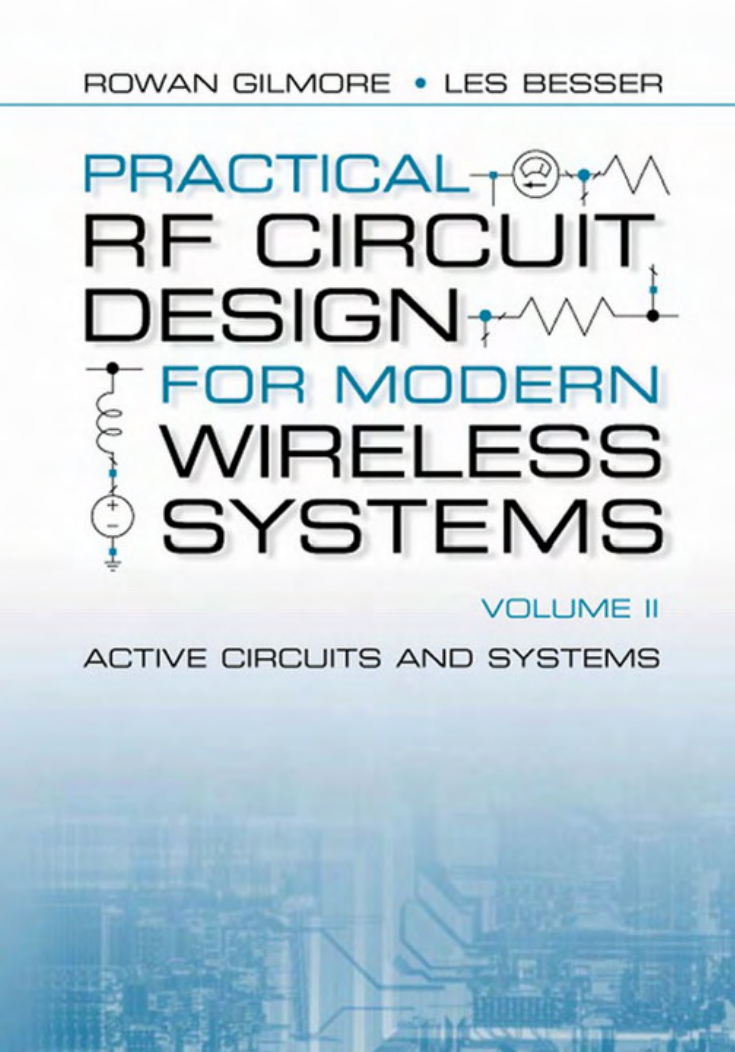
Practical RF Circuit Design for
Modern Wireless Systems
Practical RF Circuit Design for
Modern Wireless Systems
Copyright
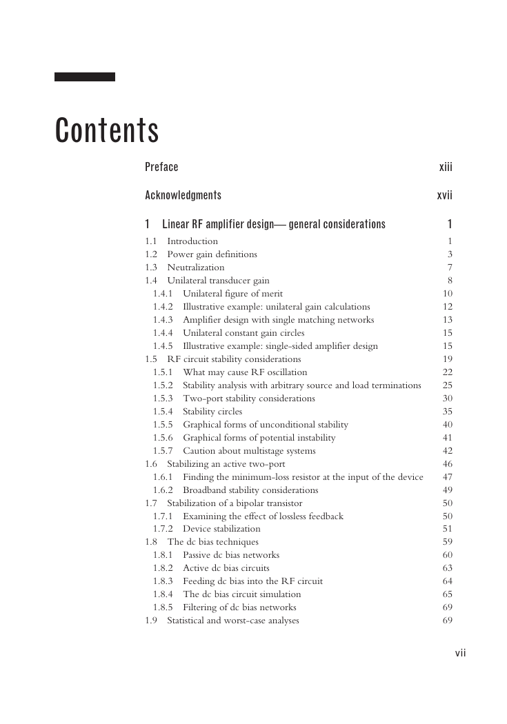
Contents
Preface
Acknowledgments
1 Linear RF amplifier design— general considerations
1.1 Introduction
1.2 Power gain definitions
1.3 Neutralization
1.4 Unilateral transducer gain
1.4.1 Unilateral figure of merit
1.4.2 Illustrative example: unilateral gain calculations
1.4.3 Amplifier design with single matching networks
1.4.4 Unilateral constant gain circles
1.4.5 Illustrative example: single- sided amplifier design
1.5 RF circuit stability considerations
1.5.1 What may cause RF oscillation
1.5.2 Stability analysis with arbitrary source and load terminations
1.5.3 Two- port stability considerations
1.5.4 Stability circles
1.5.5 Graphical forms of unconditional stability
1.5.6 Graphical forms of potential instability
1.5.7 Caution about multistage systems
1.6 Stabilizing an active two- port
1.6.1 Finding the minimum- loss resistor at the input of the device
1.6.2 Broadband stability considerations
1.7 Stabilization of a bipolar transistor
1.7.1 Examining the effect of lossless feedback
1.7.2 Device stabilization
1.8 The dc bias techniques
1.8.1 Passive dc bias networks
1.8.2 Active dc bias circuits
1.8.3 Feeding dc bias into the RF circuit
1.8.4 The dc bias circuit simulation
1.8.5 Filtering of dc bias networks
1.9 Statistical and worst- case analyses
1.10 Circuit layout considerations
1.11 Summary
1.12 Problems
2 Linear and low-noise RF amplifiers
2.1 Introduction
2.2 Bilateral RF amplifier design for maximum small- signal gain
2.2.1 Illustrative exercise: amplifier design for maximum gain, G
2.3 Multistage amplifiers
2.3.1 Cascading impedance- matched stages
2.3.2 Cascading amplifiers by direct impedance matching
2.3.3 Output power and impedance match considerations of cascaded amplifiers
2.4 Operating gain design for maximum linear output power
2.4.1 Operating gain design outline
2.4.2 G versus P trade- offs
2.4.3 Stability considerations
2.4.4 Illustrative example: operating gain design for maximum linear power output
2.4.5 Output match considerations
2.5 Noise in RF circuits
2.5.1 Review of noise sources in RF systems
2.5.2 Two- port noise parameter definitions
2.6 Available gain design technique
2.6.1 Available gain design outline
2.6.2 Low- noise amplifier design considerations
2.6.3 Illustrative example: design of a single- ended 1.9- GHz LNA
2.6.4 Balanced amplifiers
2.6.5 Illustrative example: design of a balanced LNA for the 1.7- to 2.3- GHz frequency range
2.7 Comparison of the various amplifier designs and Smith chart ¨C based graphical design aids
2.8 Broadband amplifiers
2.8.1 Reactive match/ mismatch approach
2.8.2 Dissipative mismatch at input and/ or output ports
2.8.3 Amplifier- equalizer combinations
2.8.4 Feedback amplifiers
2.8.5 Distributed amplifiers
2.9 Summary
2.10 Problems
3 Active RF devices and their modeling
3.1 The diode model
3.2 Two- port device models
3.2.2 The bipolar transistor
3.2.3 The heterojunction bipolar transistor
3.2.4 The GaAs MESFET
3.2.5 The high- electron mobility transistor
3.2.6 Silicon LDMOS and CMOS technologies
3.3 Problems
4 Nonlinear circuit simulation techniques
4.1 Classification of nonlinear circuit simulators
4.1.1 Analytical methods
4.1.2 Time- domain methods
4.1.3 Hybrid time- and frequency- domain techniques ¡ª harmonic balance
4.1.4 Frequency- domain techniques
4.2 The harmonic balance method
4.3 Harmonic balance analysis of oscillators
4.3.1 Oscillator analysis using probes
4.3.2 Oscillator analysis using reflection coefficients of the device and resonant load
4.3.3 Oscillator analysis using a directional coupler to measure open- loop gain
5 High-power RF transistor amplifier design
5.1 Nonlinear concepts
5.1.1 Some nonlinear phenomena
5.2 Quasi- linear power amplifier design
5.2.1 The amplifier load line
5.2.2 Load pull methods
5.3 Categories of amplifiers
5.3.1 Class- A amplifier
5.3.2 Class- B amplifier
5.3.3 Class- F amplifier
5.3.4 Comparison of class- A, class- B, class- F, and other operational modes
5.3.5 Switching- mode amplifiers
5.3.6 Cascaded power amplifier design
5.4 Power amplifier design example
5.4.1 Transistor selection
5.4.2 Transistor characterization
5.4.3 Matching the input and output of the device
5.4.4 Harmonic tuning example
5.5 Bias considerations
5.5.1 Bias changes at the input
5.5.2 Bias changes at the output
5.5.3 Bias considerations with power devices
5.6 Distortion reduction
5.6.1 The importance of amplifier linearity
5.6.2 Operating the amplifier backed off
5.6.3 Predistortion
5.6.4 Feedforward cancellation
5.6.5 Device modification
5.6.6 System- level reduction of distortion
5.7 Problems
6 Oscillators
6.1 Principles of oscillator design
6.1.1 Two- port oscillator design approach
6.1.2 One- port oscillator design approach
6.1.3 Transistor oscillator configurations
6.1.4 Characterizing oscillator phase noise
6.2 Oscillator design examples
6.2.1 45.455- MHz Colpitts crystal oscillator design
6.2.2 Design of a 3.7- to 4.2- GHz voltage- controlled oscillator
6.3 Problems
7 Mixers and frequency multipliers
7.1 Mixer overview and their applications in systems
7.2 Diode mixers and their topologies
7.2.1 Single- ended mixer
7.2.2 Single- balanced mixer
7.2.3 Double- balanced mixer
7.2.4 The image problem in mixers
7.2.5 Harmonic components in mixers
7.3 Transistor mixer design
7.3.1 Active transistor mixers
7.3.2 Resistive FET mixers
7.3.3 Dual- gate FET mixers
7.3.4 Comparison of mixers
7.4 Frequency multipliers ¡ª an overview
7.4.1 Frequency doublers
7.4.2 Arbitrary frequency multiplication
7.5 Problems
8 Circuits in systems—radio system applications
8.1 Mobile telephony systems
8.1.1 Second generation mobile systems
8.1.2 Third generation mobile systems
8.2 Software- defined radio
8.2.1 RF digital processing
8.2.2 Digital processing of a wideband IF
8.2.3 Digital processing at baseband ( direct conversion)
8.2.4 Transceiver issues associated with software- defined radio
8.3 A 1.9- GHz radio chip set: design overview
8.3.1 The air interface specification for PHS
8.3.2 Component specification
8.3.3 Component design
8.4 Integrated system chips: an overview
8.4.1 RF receiver front ends
8.4.2 RF upconverters and transmitter driver amplifiers
8.4.3 Transceiver and complete radio solutions
8.4.4 Power amplifier modules
8.5 Conclusion
Appendix
Summary of Basic Formulas ¨C 1
Summary of Basic Formulas ¨C 2
About the Authors
Index






 2023年江西萍乡中考道德与法治真题及答案.doc
 2012年重庆南川中考生物真题及答案.doc
 2013年江西师范大学地理学综合及文艺理论基础考研真题.doc
 2020年四川甘孜小升初语文真题及答案I卷.doc
 2020年注册岩土工程师专业基础考试真题及答案.doc
 2023-2024学年福建省厦门市九年级上学期数学月考试题及答案.doc
 2021-2022学年辽宁省沈阳市大东区九年级上学期语文期末试题及答案.doc
 2022-2023学年北京东城区初三第一学期物理期末试卷及答案.doc
 2018上半年江西教师资格初中地理学科知识与教学能力真题及答案.doc
 2012年河北国家公务员申论考试真题及答案-省级.doc
 2020-2021学年江苏省扬州市江都区邵樊片九年级上学期数学第一次质量检测试题及答案.doc
 2022下半年黑龙江教师资格证中学综合素质真题及答案.doc