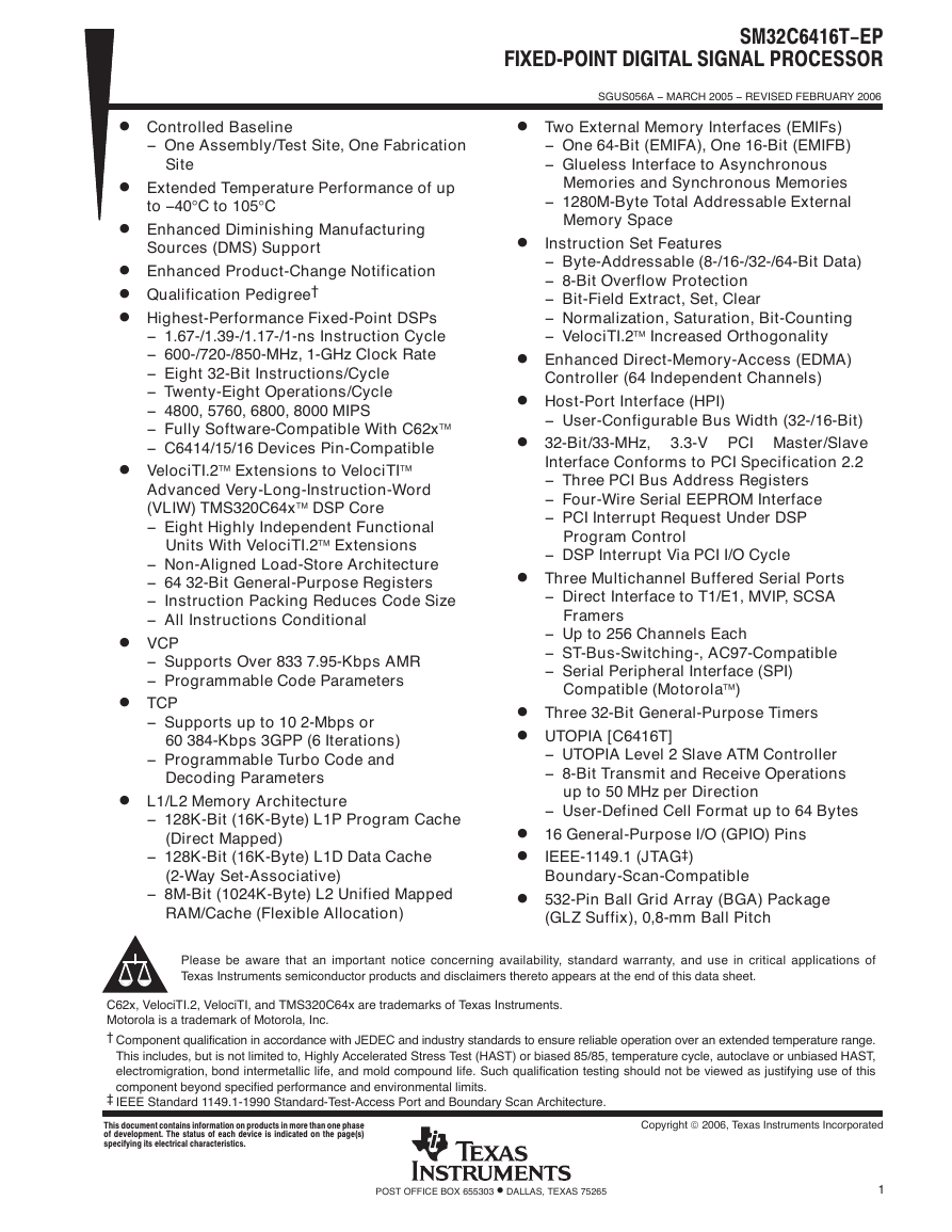
D Controlled Baseline
− One Assembly/Test Site, One Fabrication
Site
D Extended Temperature Performance of up
to −40°C to 105°C
D Enhanced Diminishing Manufacturing
Sources (DMS) Support
D Enhanced Product-Change Notification
D Qualification Pedigree†
D Highest-Performance Fixed-Point DSPs
− 1.67-/1.39-/1.17-/1-ns Instruction Cycle
− 600-/720-/850-MHz, 1-GHz Clock Rate
− Eight 32-Bit Instructions/Cycle
− Twenty-Eight Operations/Cycle
− 4800, 5760, 6800, 8000 MIPS
− Fully Software-Compatible With C62x
− C6414/15/16 Devices Pin-Compatible
D VelociTI.2 Extensions to VelociTI
Advanced Very-Long-Instruction-Word
(VLIW) TMS320C64x DSP Core
− Eight Highly Independent Functional
Units With VelociTI.2 Extensions
− Non-Aligned Load-Store Architecture
− 64 32-Bit General-Purpose Registers
− Instruction Packing Reduces Code Size
− All Instructions Conditional
D VCP
− Supports Over 833 7.95-Kbps AMR
− Programmable Code Parameters
D TCP
− Supports up to 10 2-Mbps or
60 384-Kbps 3GPP (6 Iterations)
− Programmable Turbo Code and
Decoding Parameters
D L1/L2 Memory Architecture
− 128K-Bit (16K-Byte) L1P Program Cache
(Direct Mapped)
− 128K-Bit (16K-Byte) L1D Data Cache
(2-Way Set-Associative)
− 8M-Bit (1024K-Byte) L2 Unified Mapped
RAM/Cache (Flexible Allocation)
SM32C6416T-EP
FIXEDĆPOINT DIGITAL SIGNAL PROCESSOR
SGUS056A − MARCH 2005 − REVISED FEBRUARY 2006
D Two External Memory Interfaces (EMIFs)
− One 64-Bit (EMIFA), One 16-Bit (EMIFB)
− Glueless Interface to Asynchronous
Memories and Synchronous Memories
− 1280M-Byte Total Addressable External
Memory Space
D Instruction Set Features
− Byte-Addressable (8-/16-/32-/64-Bit Data)
− 8-Bit Overflow Protection
− Bit-Field Extract, Set, Clear
− Normalization, Saturation, Bit-Counting
− VelociTI.2 Increased Orthogonality
D Enhanced Direct-Memory-Access (EDMA)
Controller (64 Independent Channels)
D Host-Port Interface (HPI)
− User-Configurable Bus Width (32-/16-Bit)
D 32-Bit/33-MHz, 3.3-V PCI Master/Slave
Interface Conforms to PCI Specification 2.2
− Three PCI Bus Address Registers
− Four-Wire Serial EEPROM Interface
− PCI Interrupt Request Under DSP
Program Control
− DSP Interrupt Via PCI I/O Cycle
D Three Multichannel Buffered Serial Ports
− Direct Interface to T1/E1, MVIP, SCSA
Framers
− Up to 256 Channels Each
− ST-Bus-Switching-, AC97-Compatible
− Serial Peripheral Interface (SPI)
Compatible (Motorola)
D Three 32-Bit General-Purpose Timers
D UTOPIA [C6416T]
− UTOPIA Level 2 Slave ATM Controller
− 8-Bit Transmit and Receive Operations
up to 50 MHz per Direction
− User-Defined Cell Format up to 64 Bytes
D 16 General-Purpose I/O (GPIO) Pins
D IEEE-1149.1 (JTAG‡)
Boundary-Scan-Compatible
D 532-Pin Ball Grid Array (BGA) Package
(GLZ Suffix), 0,8-mm Ball Pitch
Please be aware that an important notice concerning availability, standard warranty, and use in critical applications of
Texas Instruments semiconductor products and disclaimers thereto appears at the end of this data sheet.
C62x, VelociTI.2, VelociTI, and TMS320C64x are trademarks of Texas Instruments.
Motorola is a trademark of Motorola, Inc.
† Component qualification in accordance with JEDEC and industry standards to ensure reliable operation over an extended temperature range.
This includes, but is not limited to, Highly Accelerated Stress Test (HAST) or biased 85/85, temperature cycle, autoclave or unbiased HAST,
electromigration, bond intermetallic life, and mold compound life. Such qualification testing should not be viewed as justifying use of this
component beyond specified performance and environmental limits.
‡ IEEE Standard 1149.1-1990 Standard-Test-Access Port and Boundary Scan Architecture.
This document contains information on products in more than one phase
of development. The status of each device is indicated on the page(s)
specifying its electrical characteristics.
Copyright 2006, Texas Instruments Incorporated
POST OFFICE BOX 655303 • DALLAS, TEXAS 75265
1
�
SM32C6416T-EP
FIXEDĆPOINT DIGITAL SIGNAL PROCESSOR
SGUS056A − MARCH 2005 − REVISED FEBRUARY 2006
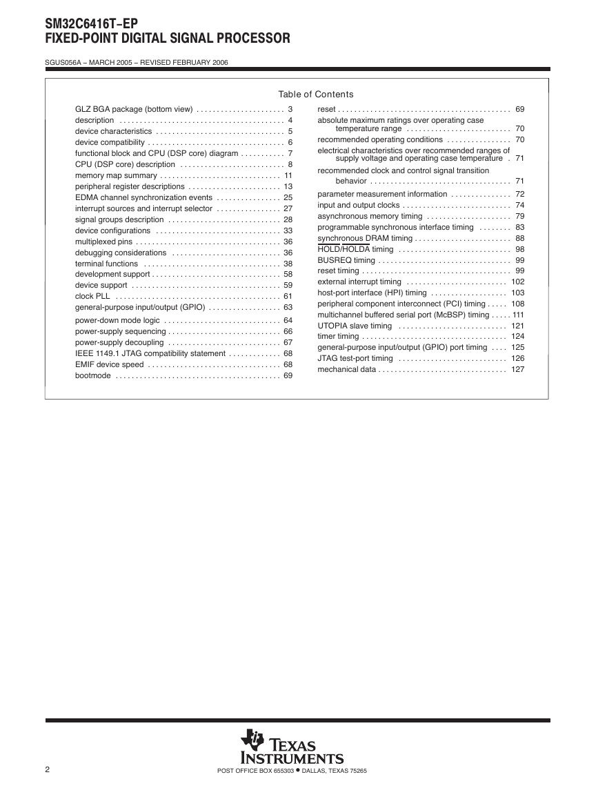
Table of Contents
GLZ BGA package (bottom view)
description
device characteristics
device compatibility
functional block and CPU (DSP core) diagram
CPU (DSP core) description
memory map summary
peripheral register descriptions
EDMA channel synchronization events
interrupt sources and interrupt selector
signal groups description
device configurations
multiplexed pins
debugging considerations
terminal functions
development support
device support
clock PLL
general-purpose input/output (GPIO)
power-down mode logic
power-supply sequencing
power-supply decoupling
IEEE 1149.1 JTAG compatibility statement
EMIF device speed
bootmode
. . . . . . . . . . . . . . . . . . . . . .
. . . . . . . . . . . . . . . . . . . . . . . . . . . . . . . . . . . . . . . . .
. . . . . . . . . . . . . . . . . . . . . . . . . . . . . . . .
. . . . . . . . . . . . . . . . . . . . . . . . . . . . . . . . . .
. . . . . . . . . . .
. . . . . . . . . . . . . . . . . . . . . . . . . .
. . . . . . . . . . . . . . . . . . . . . . . . . . . . . .
. . . . . . . . . . . . . . . . . . . . . . .
. . . . . . . . . . . . . . . .
. . . . . . . . . . . . . . . .
. . . . . . . . . . . . . . . . . . . . . . . . . . . .
. . . . . . . . . . . . . . . . . . . . . . . . . . . . . . .
. . . . . . . . . . . . . . . . . . . . . . . . . . . . . . . . . . . .
. . . . . . . . . . . . . . . . . . . . . . . . . . .
. . . . . . . . . . . . . . . . . . . . . . . . . . . . . . . . . .
. . . . . . . . . . . . . . . . . . . . . . . . . . . . . . . .
. . . . . . . . . . . . . . . . . . . . . . . . . . . . . . . . . . . . .
. . . . . . . . . . . . . . . . . . . . . . . . . . . . . . . . . . . . . . . . .
. . . . . . . . . . . . . . . . . .
. . . . . . . . . . . . . . . . . . . . . . . . . . . . .
. . . . . . . . . . . . . . . . . . . . . . . . . . . .
. . . . . . . . . . . . . . . . . . . . . . . . . . . .
. . . . . . . . . . . . .
. . . . . . . . . . . . . . . . . . . . . . . . . . . . . . . . .
. . . . . . . . . . . . . . . . . . . . . . . . . . . . . . . . . . . . . . . . .
3
4
5
6
7
8
11
13
25
27
28
33
36
36
38
58
59
61
63
64
66
67
68
68
69
. . . . . . . . . . . . . . . . . . . . . . . . . . . . . . . . . . . . . . . . . . .
reset
absolute maximum ratings over operating case
temperature range
. . . . . . . . . . . . . . . . . . . . . . . . . .
recommended operating conditions
. . . . . . . . . . . . . . . .
electrical characteristics over recommended ranges of
.
supply voltage and operating case temperature
69
70
70
71
recommended clock and control signal transition
behavior
parameter measurement information
input and output clocks
asynchronous memory timing
programmable synchronous interface timing
synchronous DRAM timing
HOLD/HOLDA timing
BUSREQ timing
reset timing
external interrupt timing
host-port interface (HPI) timing
peripheral component interconnect (PCI) timing
multichannel buffered serial port (McBSP) timing
UTOPIA slave timing
timer timing
general-purpose input/output (GPIO) port timing
JTAG test-port timing
mechanical data
. . . . . . . . . . . . . . . . . . . . . . . . . . . . . . . . . . .
. . . . . . . . . . . . . . .
. . . . . . . . . . . . . . . . . . . . . . . . . . .
. . . . . . . . . . . . . . . . . . . . .
. . . . . . . .
. . . . . . . . . . . . . . . . . . . . . . . .
. . . . . . . . . . . . . . . . . . . . . . . . . . . .
. . . . . . . . . . . . . . . . . . . . . . . . . . . . . . . . .
. . . . . . . . . . . . . . . . . . . . . . . . . . . . . . . . . . . . .
. . . . . . . . . . . . . . . . . . . . . . . . .
. . . . . . . . . . . . . . . . . . .
. . . . .
. . . . .
. . . . . . . . . . . . . . . . . . . . . . . . . . .
. . . . . . . . . . . . . . . . . . . . . . . . . . . . . . . . . . . .
. . . .
. . . . . . . . . . . . . . . . . . . . . . . . . . .
. . . . . . . . . . . . . . . . . . . . . . . . . . . . . . . .
71
72
74
79
83
88
98
99
99
102
103
108
111
121
124
125
126
127
2
POST OFFICE BOX 655303 • DALLAS, TEXAS 75265
�
SM32C6416T-EP
FIXEDĆPOINT DIGITAL SIGNAL PROCESSOR
SGUS056A − MARCH 2005 − REVISED FEBRUARY 2006
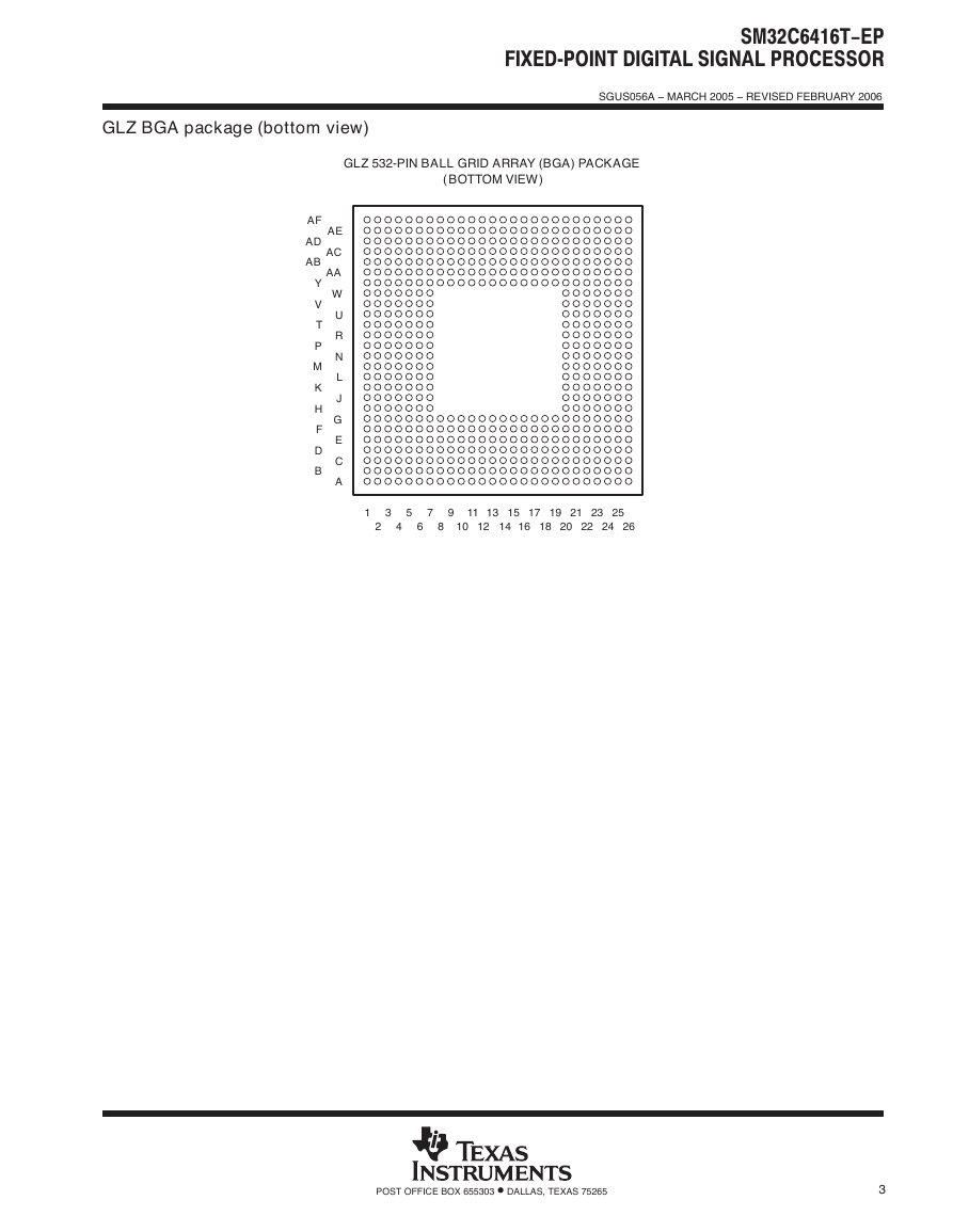
GLZ BGA package (bottom view)
GLZ 532-PIN BALL GRID ARRAY (BGA) PACKAGE
( BOTTOM VIEW )
AF
AD
AB
Y
V
T
P
M
K
H
F
D
B
AE
AC
AA
W
U
R
N
L
J
G
E
C
A
1
3
5
7
9
11
13
15
17
19
21
23
25
2
4
6
8
10
12
14
16
18
20
22
24
26
POST OFFICE BOX 655303 • DALLAS, TEXAS 75265
3
�
SM32C6416T-EP
FIXEDĆPOINT DIGITAL SIGNAL PROCESSOR
SGUS056A − MARCH 2005 − REVISED FEBRUARY 2006
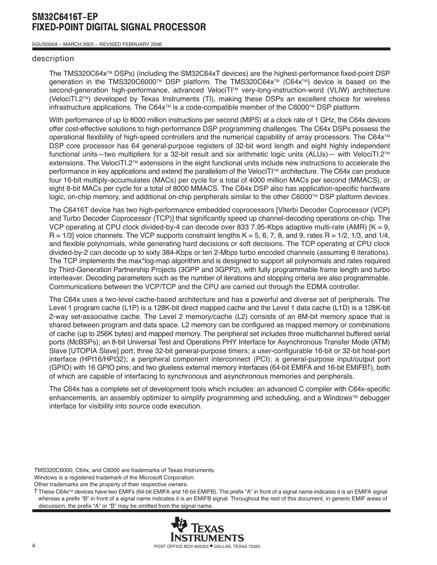
description
The TMS320C64x DSPs) (including the SM32C64xT devices) are the highest-performance fixed-point DSP
generation in the TMS320C6000 DSP platform. The TMS320C64x (C64x) device is based on the
second-generation high-performance, advanced VelociTI very-long-instruction-word (VLIW) architecture
(VelociTI.2) developed by Texas Instruments (TI), making these DSPs an excellent choice for wireless
infrastructure applications. The C64x is a code-compatible member of the C6000 DSP platform.
With performance of up to 8000 million instructions per second (MIPS) at a clock rate of 1 GHz, the C64x devices
offer cost-effective solutions to high-performance DSP programming challenges. The C64x DSPs possess the
operational flexibility of high-speed controllers and the numerical capability of array processors. The C64x
DSP core processor has 64 general-purpose registers of 32-bit word length and eight highly independent
functional units—two multipliers for a 32-bit result and six arithmetic logic units (ALUs)— with VelociTI.2
extensions. The VelociTI.2 extensions in the eight functional units include new instructions to accelerate the
performance in key applications and extend the parallelism of the VelociTI architecture. The C64x can produce
four 16-bit multiply-accumulates (MACs) per cycle for a total of 4000 million MACs per second (MMACS), or
eight 8-bit MACs per cycle for a total of 8000 MMACS. The C64x DSP also has application-specific hardware
logic, on-chip memory, and additional on-chip peripherals similar to the other C6000 DSP platform devices.
The C6416T device has two high-performance embedded coprocessors [Viterbi Decoder Coprocessor (VCP)
and Turbo Decoder Coprocessor (TCP)] that significantly speed up channel-decoding operations on-chip. The
VCP operating at CPU clock divided-by-4 can decode over 833 7.95-Kbps adaptive multi-rate (AMR) [K = 9,
R = 1/3] voice channels. The VCP supports constraint lengths K = 5, 6, 7, 8, and 9, rates R = 1/2, 1/3, and 1/4,
and flexible polynomials, while generating hard decisions or soft decisions. The TCP operating at CPU clock
divided-by-2 can decode up to sixty 384-Kbps or ten 2-Mbps turbo encoded channels (assuming 6 iterations).
The TCP implements the max*log-map algorithm and is designed to support all polynomials and rates required
by Third-Generation Partnership Projects (3GPP and 3GPP2), with fully programmable frame length and turbo
interleaver. Decoding parameters such as the number of iterations and stopping criteria are also programmable.
Communications between the VCP/TCP and the CPU are carried out through the EDMA controller.
The C64x uses a two-level cache-based architecture and has a powerful and diverse set of peripherals. The
Level 1 program cache (L1P) is a 128K-bit direct mapped cache and the Level 1 data cache (L1D) is a 128K-bit
2-way set-associative cache. The Level 2 memory/cache (L2) consists of an 8M-bit memory space that is
shared between program and data space. L2 memory can be configured as mapped memory or combinations
of cache (up to 256K bytes) and mapped memory. The peripheral set includes three multichannel buffered serial
ports (McBSPs); an 8-bit Universal Test and Operations PHY Interface for Asynchronous Transfer Mode (ATM)
Slave [UTOPIA Slave] port; three 32-bit general-purpose timers; a user-configurable 16-bit or 32-bit host-port
interface (HPI16/HPI32); a peripheral component interconnect (PCI); a general-purpose input/output port
(GPIO) with 16 GPIO pins; and two glueless external memory interfaces (64-bit EMIFA and 16-bit EMIFB†), both
of which are capable of interfacing to synchronous and asynchronous memories and peripherals.
The C64x has a complete set of development tools which includes: an advanced C compiler with C64x-specific
enhancements, an assembly optimizer to simplify programming and scheduling, and a Windows debugger
interface for visibility into source code execution.
TMS320C6000, C64x, and C6000 are trademarks of Texas Instruments.
Windows is a registered trademark of the Microsoft Corporation.
Other trademarks are the property of their respective owners.
† These C64x devices have two EMIFs (64-bit EMIFA and 16-bit EMIFB). The prefix “A” in front of a signal name indicates it is an EMIFA signal
whereas a prefix “B” in front of a signal name indicates it is an EMIFB signal. Throughout the rest of this document, in generic EMIF areas of
discussion, the prefix “A” or “B” may be omitted from the signal name.
4
POST OFFICE BOX 655303 • DALLAS, TEXAS 75265
�
SM32C6416T-EP
FIXEDĆPOINT DIGITAL SIGNAL PROCESSOR
SGUS056A − MARCH 2005 − REVISED FEBRUARY 2006
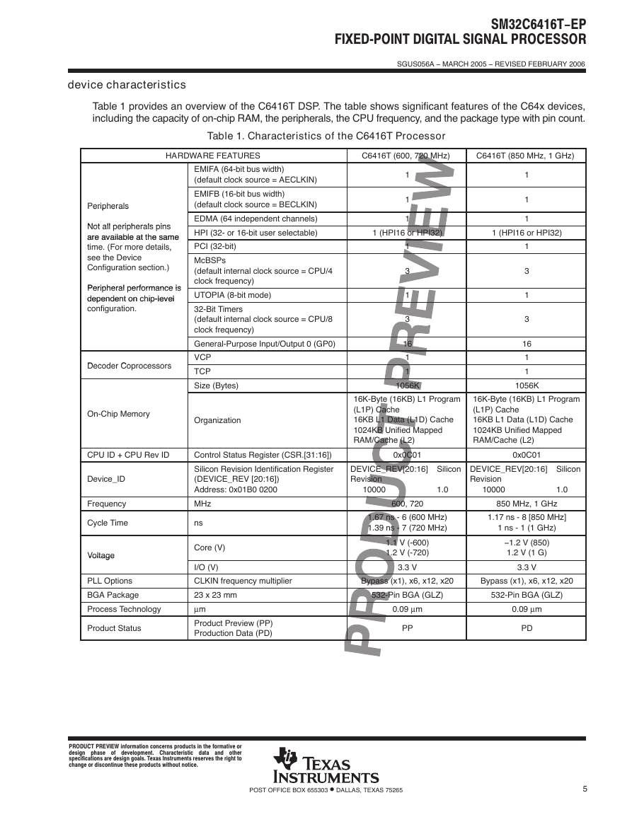
device characteristics
Table 1 provides an overview of the C6416T DSP. The table shows significant features of the C64x devices,
including the capacity of on-chip RAM, the peripherals, the CPU frequency, and the package type with pin count.
Table 1. Characteristics of the C6416T Processor
HARDWARE FEATURES
C6416T (600, 720 MHz)
C6416T (850 MHz, 1 GHz)
Peripherals
Peripherals
Not all peripherals pins
Not all peripherals pins
are available at the same
are available at the same
time. (For more details,
time. (For more details,
see the Device
see the Device
Configuration section.)
Peripheral performance is
Peripheral performance is
dependent on chip-level
dependent on chip-level
configuration.
Decoder Coprocessors
Decoder Coprocessors
EMIFA (64-bit bus width)
(default clock source = AECLKIN)
EMIFB (16-bit bus width)
(default clock source = BECLKIN)
EDMA (64 independent channels)
HPI (32- or 16-bit user selectable)
PCI (32-bit)
McBSPs
(default internal clock source = CPU/4
clock frequency)
UTOPIA (8-bit mode)
32-Bit Timers
(default internal clock source = CPU/8
clock frequency)
General-Purpose Input/Output 0 (GP0)
VCP
TCP
Size (Bytes)
On-Chip Memory
Organization
CPU ID + CPU Rev ID
Device_ID
Frequency
Cycle Time
Voltage
Voltage
PLL Options
BGA Package
Process Technology
Product Status
Control Status Register (CSR.[31:16])
Silicon Revision Identification Register
(DEVICE_REV [20:16])
Address: 0x01B0 0200
MHz
ns
Core (V)
I/O (V)
CLKIN frequency multiplier
23 x 23 mm
µm
Product Preview (PP)
Production Data (PD)
1
1
1
1
1
1
1 (HPI16 or HPI32)
1 (HPI16 or HPI32)
1
3
1
3
16
1
1
1
3
1
3
16
1
1
1056K
1056K
16K-Byte (16KB) L1 Program
(L1P) Cache
16KB L1 Data (L1D) Cache
1024KB Unified Mapped
RAM/Cache (L2)
16K-Byte (16KB) L1 Program
(L1P) Cache
16KB L1 Data (L1D) Cache
1024KB Unified Mapped
RAM/Cache (L2)
0x0C01
0x0C01
DEVICE_REV[20:16] Silicon
Revision
10000
1.0
DEVICE_REV[20:16] Silicon
Revision
10000
1.0
600, 720
1.67 ns - 6 (600 MHz)
1.39 ns - 7 (720 MHz)
850 MHz, 1 GHz
1.17 ns - 8 [850 MHz]
1 ns - 1 (1 GHz)
1.1 V (-600)
1.2 V (-720)
3.3 V
−1.2 V (850)
1.2 V (1 G)
3.3 V
Bypass (x1), x6, x12, x20
Bypass (x1), x6, x12, x20
532-Pin BGA (GLZ)
532-Pin BGA (GLZ)
0.09 µm
PP
0.09 µm
PD
PRODUCT PREVIEW information concerns products in the formative or
design phase of development. Characteristic data and other
specifications are design goals. Texas Instruments reserves the right to
change or discontinue these products without notice.
POST OFFICE BOX 655303 • DALLAS, TEXAS 75265
5
�
SM32C6416T-EP
FIXEDĆPOINT DIGITAL SIGNAL PROCESSOR
SGUS056A − MARCH 2005 − REVISED FEBRUARY 2006
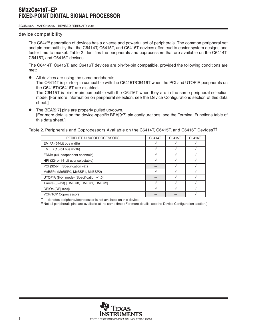
device compatibility
The C64x generation of devices has a diverse and powerful set of peripherals. The common peripheral set
and pin-compatibility that the C6414T, C6415T, and C6416T devices offer lead to easier system designs and
faster time to market. Table 2 identifies the peripherals and coprocessors that are available on the C6414T,
C6415T, and C6416T devices.
The C6414T, C6415T, and C6416T devices are pin-for-pin compatible, provided the following conditions are
met:
D All devices are using the same peripherals.
The C6414T is pin-for-pin compatible with the C6415T/C6416T when the PCI and UTOPIA peripherals on
the C6415T/C6416T are disabled.
The C6415T is pin-for-pin compatible with the C6416T when they are in the same peripheral selection
mode. [For more information on peripheral selection, see the Device Configurations section of this data
sheet.]
D The BEA[9:7] pins are properly pulled up/down.
[For more details on the device-specific BEA[9:7] pin configurations, see the Terminal Functions table of
this data sheet.]
Table 2. Peripherals and Coprocessors Available on the C6414T, C6415T, and C6416T Devices†‡
PERIPHERALS/COPROCESSORS
C6414T
C6415T
C6416T
EMIFA (64-bit bus width)
EMIFB (16-bit bus width)
EDMA (64 independent channels)
HPI (32- or 16-bit user selectable)
PCI (32-bit) [Specification v2.2]
McBSPs (McBSP0, McBSP1, McBSP2)
UTOPIA (8-bit mode) [Specification v1.0]
Timers (32-bit) [TIMER0, TIMER1, TIMER2]
GPIOs (GP[15:0])
VCP/TCP Coprocessors
√
√
√
√
—
√
—
√
√
—
√
√
√
√
√
√
√
√
√
—
√
√
√
√
√
√
√
√
√
√
† — denotes peripheral/coprocessor is not available on this device.
‡ Not all peripherals pins are available at the same time. (For more details, see the Device Configuration section.)
6
POST OFFICE BOX 655303 • DALLAS, TEXAS 75265
�
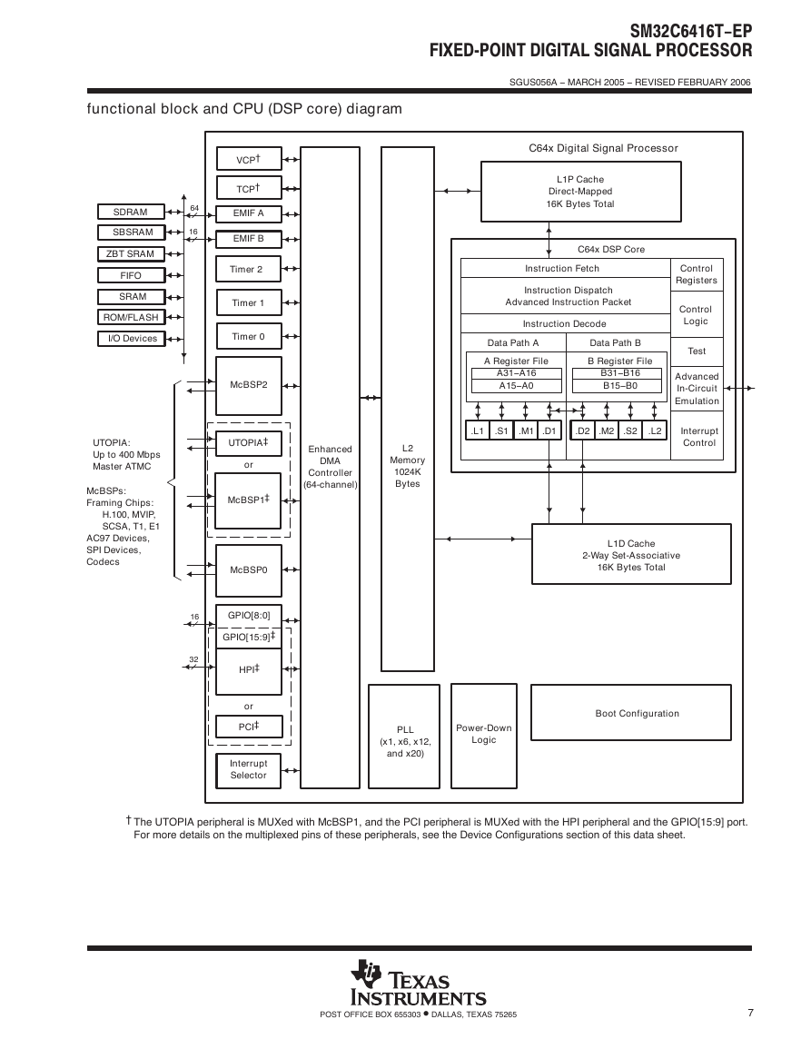
functional block and CPU (DSP core) diagram
SM32C6416T-EP
FIXEDĆPOINT DIGITAL SIGNAL PROCESSOR
SGUS056A − MARCH 2005 − REVISED FEBRUARY 2006
SDRAM
SBSRAM
ZBT SRAM
FIFO
SRAM
ROM/FLASH
I/O Devices
UTOPIA:
Up to 400 Mbps
Master ATMC
McBSPs:
Framing Chips:
H.100, MVIP,
SCSA, T1, E1
AC97 Devices,
SPI Devices,
Codecs
64
16
16
32
VCP†
TCP†
EMIF A
EMIF B
Timer 2
Timer 1
Timer 0
McBSP2
UTOPIA‡
or
McBSP1‡
McBSP0
GPIO[8:0]
GPIO[15:9]‡
HPI‡
or
PCI‡
Interrupt
Selector
C64x Digital Signal Processor
L1P Cache
Direct-Mapped
16K Bytes Total
C64x DSP Core
Instruction Fetch
Instruction Dispatch
Advanced Instruction Packet
Instruction Decode
Data Path A
Data Path B
A Register File
B Register File
A31−A16
A15−A0
B31−B16
B15−B0
.L1
.S1 .M1 .D1
.D2 .M2 .S2
.L2
Control
Registers
Control
Logic
Test
Advanced
In-Circuit
Emulation
Interrupt
Control
L1D Cache
2-Way Set-Associative
16K Bytes Total
Enhanced
DMA
Controller
(64-channel)
L2
Memory
1024K
Bytes
PLL
(x1, x6, x12,
and x20)
Power-Down
Logic
Boot Configuration
† The UTOPIA peripheral is MUXed with McBSP1, and the PCI peripheral is MUXed with the HPI peripheral and the GPIO[15:9] port.
For more details on the multiplexed pins of these peripherals, see the Device Configurations section of this data sheet.
POST OFFICE BOX 655303 • DALLAS, TEXAS 75265
7
�
SM32C6416T-EP
FIXEDĆPOINT DIGITAL SIGNAL PROCESSOR
SGUS056A − MARCH 2005 − REVISED FEBRUARY 2006
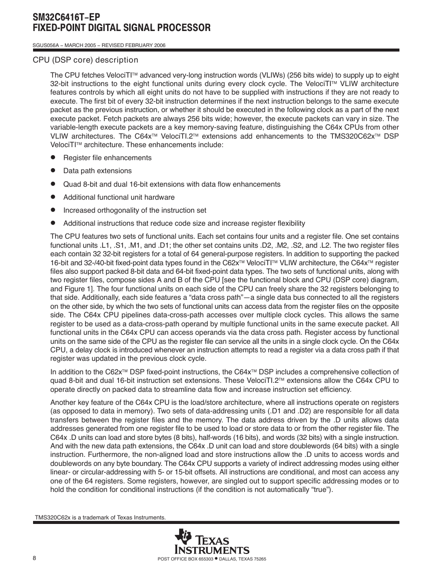
CPU (DSP core) description
The CPU fetches VelociTI advanced very-long instruction words (VLIWs) (256 bits wide) to supply up to eight
32-bit instructions to the eight functional units during every clock cycle. The VelociTI VLIW architecture
features controls by which all eight units do not have to be supplied with instructions if they are not ready to
execute. The first bit of every 32-bit instruction determines if the next instruction belongs to the same execute
packet as the previous instruction, or whether it should be executed in the following clock as a part of the next
execute packet. Fetch packets are always 256 bits wide; however, the execute packets can vary in size. The
variable-length execute packets are a key memory-saving feature, distinguishing the C64x CPUs from other
VLIW architectures. The C64x VelociTI.2 extensions add enhancements to the TMS320C62x DSP
VelociTI architecture. These enhancements include:
D Register file enhancements
D Data path extensions
D Quad 8-bit and dual 16-bit extensions with data flow enhancements
D Additional functional unit hardware
D Increased orthogonality of the instruction set
D Additional instructions that reduce code size and increase register flexibility
The CPU features two sets of functional units. Each set contains four units and a register file. One set contains
functional units .L1, .S1, .M1, and .D1; the other set contains units .D2, .M2, .S2, and .L2. The two register files
each contain 32 32-bit registers for a total of 64 general-purpose registers. In addition to supporting the packed
16-bit and 32-/40-bit fixed-point data types found in the C62x VelociTI VLIW architecture, the C64x register
files also support packed 8-bit data and 64-bit fixed-point data types. The two sets of functional units, along with
two register files, compose sides A and B of the CPU [see the functional block and CPU (DSP core) diagram,
and Figure 1]. The four functional units on each side of the CPU can freely share the 32 registers belonging to
that side. Additionally, each side features a “data cross path”—a single data bus connected to all the registers
on the other side, by which the two sets of functional units can access data from the register files on the opposite
side. The C64x CPU pipelines data-cross-path accesses over multiple clock cycles. This allows the same
register to be used as a data-cross-path operand by multiple functional units in the same execute packet. All
functional units in the C64x CPU can access operands via the data cross path. Register access by functional
units on the same side of the CPU as the register file can service all the units in a single clock cycle. On the C64x
CPU, a delay clock is introduced whenever an instruction attempts to read a register via a data cross path if that
register was updated in the previous clock cycle.
In addition to the C62x DSP fixed-point instructions, the C64x DSP includes a comprehensive collection of
quad 8-bit and dual 16-bit instruction set extensions. These VelociTI.2 extensions allow the C64x CPU to
operate directly on packed data to streamline data flow and increase instruction set efficiency.
Another key feature of the C64x CPU is the load/store architecture, where all instructions operate on registers
(as opposed to data in memory). Two sets of data-addressing units (.D1 and .D2) are responsible for all data
transfers between the register files and the memory. The data address driven by the .D units allows data
addresses generated from one register file to be used to load or store data to or from the other register file. The
C64x .D units can load and store bytes (8 bits), half-words (16 bits), and words (32 bits) with a single instruction.
And with the new data path extensions, the C64x .D unit can load and store doublewords (64 bits) with a single
instruction. Furthermore, the non-aligned load and store instructions allow the .D units to access words and
doublewords on any byte boundary. The C64x CPU supports a variety of indirect addressing modes using either
linear- or circular-addressing with 5- or 15-bit offsets. All instructions are conditional, and most can access any
one of the 64 registers. Some registers, however, are singled out to support specific addressing modes or to
hold the condition for conditional instructions (if the condition is not automatically “true”).
TMS320C62x is a trademark of Texas Instruments.
8
POST OFFICE BOX 655303 • DALLAS, TEXAS 75265
�


 2023年江西萍乡中考道德与法治真题及答案.doc
 2012年重庆南川中考生物真题及答案.doc
 2013年江西师范大学地理学综合及文艺理论基础考研真题.doc
 2020年四川甘孜小升初语文真题及答案I卷.doc
 2020年注册岩土工程师专业基础考试真题及答案.doc
 2023-2024学年福建省厦门市九年级上学期数学月考试题及答案.doc
 2021-2022学年辽宁省沈阳市大东区九年级上学期语文期末试题及答案.doc
 2022-2023学年北京东城区初三第一学期物理期末试卷及答案.doc
 2018上半年江西教师资格初中地理学科知识与教学能力真题及答案.doc
 2012年河北国家公务员申论考试真题及答案-省级.doc
 2020-2021学年江苏省扬州市江都区邵樊片九年级上学期数学第一次质量检测试题及答案.doc
 2022下半年黑龙江教师资格证中学综合素质真题及答案.doc