Application Note 110
Designing a GPIB Device
Using the NAT9914
Andrew Thomson
Introduction
This application note describes how to build a GPIB device using the NAT9914 and a common microcontroller. It
discusses methods to implement GPIB commands and provides a flexible structure to build a GPIB interface into your
instrument. This application note supplements the descriptions in the NAT9914 Reference Manual of hardware and
software considerations of a GPIB device. More information about the NAT9914 and its command set and registers
can be found in the NAT9914 Reference Manual. More help on the GPIB interface itself can be found in the IEEE 488.1
and IEEE 488.2 specifications.
Appendix A contains a comprehensive tutorial on the GPIB, including a historical summary. Appendix B contains soft-
ware listings of the programs described later in this document.
Determining Performance Requirements
Several factors determine how fast a GPIB interface needs to be.
•
Amount of data transferred – a device such as a digital multimeter may transfer only a few bytes every few sec-
onds. A device such as an oscilloscope can transfer several megabytes at a time. A large amount of data requires
a faster GPIB interface.
Typical application of the device – in a production test environment, a slow device can increase testing time, there-
fore increasing testing cost. In a laboratory, an engineer might be willing to sacrifice performance because making
measurements may not be a time-critical task.
Frequency of device access – even a moderate GPIB speed will cost the user time in a test operating continually.
A GPIB device that rarely transmits data can send data slower than one that constantly sends data.
•
•
Choosing a GPIB Interface Chip
NAT9914
The NAT9914 can transmit or receive data at several kbytes/s to several hundred kbytes/s, depending on the
microcontroller. The NAT9914 is relatively easy to program, inexpensive, and versatile. The NAT9914 does need
external GPIB transceivers.
NAT9914 with Supplementary Hardware
Read “Software Considerations” in the NAT9914 Reference Manual for more detailed information on both DMA and
FIFOs. The NAT9914 can also use Direct Memory Access (DMA). A DMA controller transfers data directly between
the NAT9914 and the memory without intervention by the microcontroller.
—————————————————
Product and company names are trademarks or trade names of their respective companies.
341398A-01
© Copyright 1998 National Instruments Corporation. All rights reserved.
January 1998
�
FIFOs are simpler to interface to the NAT9914, but still increase GPIB transfer speed significantly. Using external
FIFOs, the NAT9914 can transfer more than 1 Mbytes/s.
Both a FIFO and a DMA controller, working together with a NAT9914, transfer data even faster. However, for
high-performance applications, you should choose the TNT4882, which transfers data faster and costs less.
TNT4882
The TNT4882 offers a faster interface to the GPIB. The TNT4882 also has the fast HS488 transfer capabilities and
internal FIFOs. You can transfer up to 1.5 Mbytes/s using a 488.1 handshake or up to 8 Mbytes/s using the newer
HS488 GPIB protocol. Even though the TNT4882 also has integrated GPIB transceivers and is useful for large data
transfers where speed is critical, the TNT4882 has a 9914 mode. Code written for the NAT9914 can be ported to the
TNT4882 with few modifications.
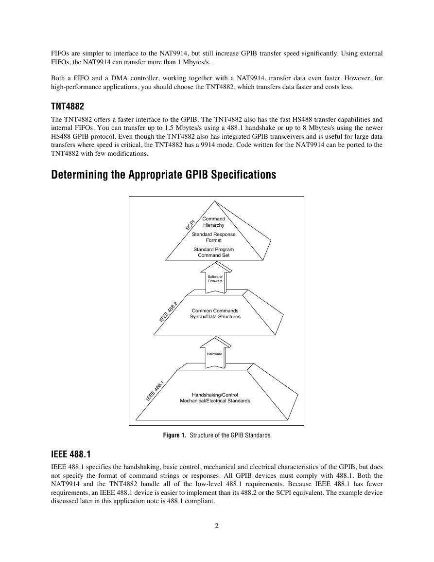
Determining the Appropriate GPIB Specifications
Command
Hierarchy
SCPI
Standard Response
Format
Standard Program
Command Set
Software/
Firmware
IEEE 488.2
Common Commands
Syntax/Data Structures
Hardware
IEEE 488.1
Handshaking/Control
Mechanical/Electrical Standards
Figure 1. Structure of the GPIB Standards
IEEE 488.1
IEEE 488.1 specifies the handshaking, basic control, mechanical and electrical characteristics of the GPIB, but does
not specify the format of command strings or responses. All GPIB devices must comply with 488.1. Both the
NAT9914 and the TNT4882 handle all of the low-level 488.1 requirements. Because IEEE 488.1 has fewer
requirements, an IEEE 488.1 device is easier to implement than its 488.2 or the SCPI equivalent. The example device
discussed later in this application note is 488.1 compliant.
2
�
IEEE 488.2
All IEEE 488.2 devices are also 488.1 devices. In addition to 488.1 requirements, IEEE 488.2 specifies data formats
for commands and responses. The specification also standardizes error handling and status reporting, and it requires
all devices to include certain commands and optionally, several more commands. Designing a 488.2 device requires
more complicated firmware, but some end users find 488.2 devices easier to program. The NAT9914 and TNT4882
both can be used in 488.2 compliant devices. IEEE 488.2 will help a user if he has other 488.2 devices or if he is
comfortable with 488.2.
SCPI
SCPI adds to the 488.2 specifications by defining a single command set for all instruments. Many major instrument
manufacturers make SCPI-compliant devices. For a complete line of oscilloscopes or other instruments with large
command sets, SCPI provides a seamless, coherent interface while standardizing the command set.
Designing a Command Set
Command Set Completeness
Your command set should enable the user to control all functions of the device. Any functionality available through
the front panel should also be available remotely.
ASCII strings
Devices generally use 7-bit ASCII strings. ASCII strings are easy to read when debugging, platform independent, and
almost universally accepted among GPIB instruments. Capital letters are required by IEEE 488.2 and commonly used
in 488.1 instruments. Some devices also send 8-bit binary data in an IEEE specified format.
Commands and Queries
A command tells the device to perform a specific task. A command does not return information. A command might
tell a device to generate voltage or set a configuration option. A query requests information from the device. A query
might request the temperature or a voltage reading.
Command Set for the Example Device
This example device parses the incoming data for an ASCII string beginning with either a “VOLT?” query or “TARE”
command. With an expanded parsing routine, this device could become 488.2 or SCPI compliant.
Designing the Hardware
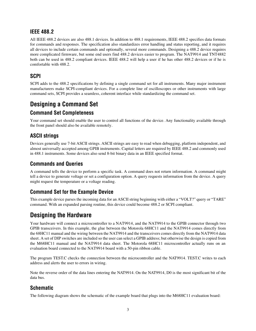
Your hardware will connect a microcontroller to a NAT9914, and the NAT9914 to the GPIB connector through two
GPIB transceivers. In this example, the glue between the Motorola 68HC11 and the NAT9914 comes directly from
the 68HC11 manual and the wiring between the NAT9914 and the transceivers comes directly from the NAT9914 data
sheet. A set of DIP switches are included so the user can select a GPIB address; but otherwise the design is copied from
the M68HC11 manual and the NAT9914 data sheet. The Motorola 68HC11 microcontroller actually runs on an
evaluation board connected to the NAT9914 board with a 50-pin ribbon cable.
The program TEST.C checks the connection between the microcontroller and the NAT9914. TEST.C writes to each
address and alerts the user to errors in wiring.
Note the reverse order of the data lines entering the NAT9914. On the NAT9914, D0 is the most significant bit of the
data bus.
Schematic
The following diagram shows the schematic of the example board that plugs into the M68HC11 evaluation board:
3
�
Figure 2. Schematic of GPIB Device
4
�
The GAL decodes the address and expands the multiplexed address/data bus of the Motorola 68HC11 so the NAT9914
appears at the M68HC11 memory address 0x1080. The following abel code defines the behavior of the GAL:
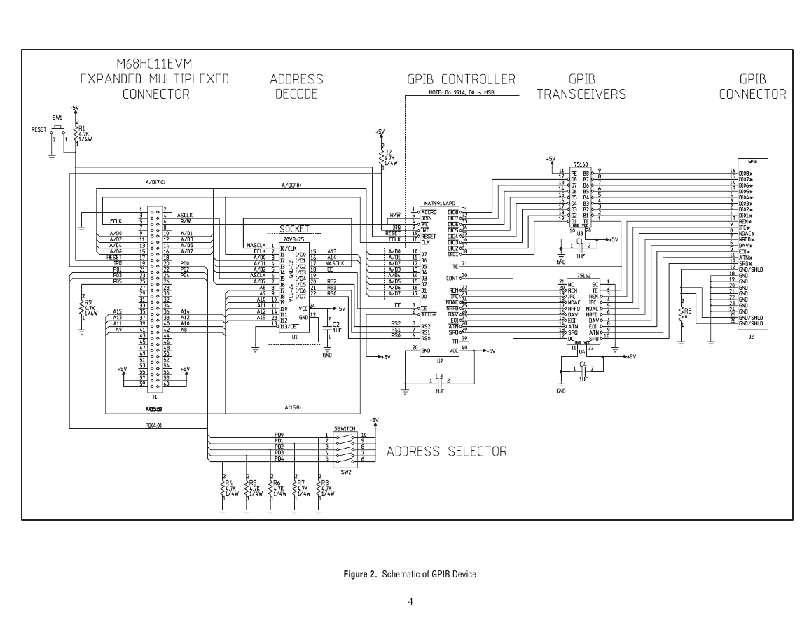
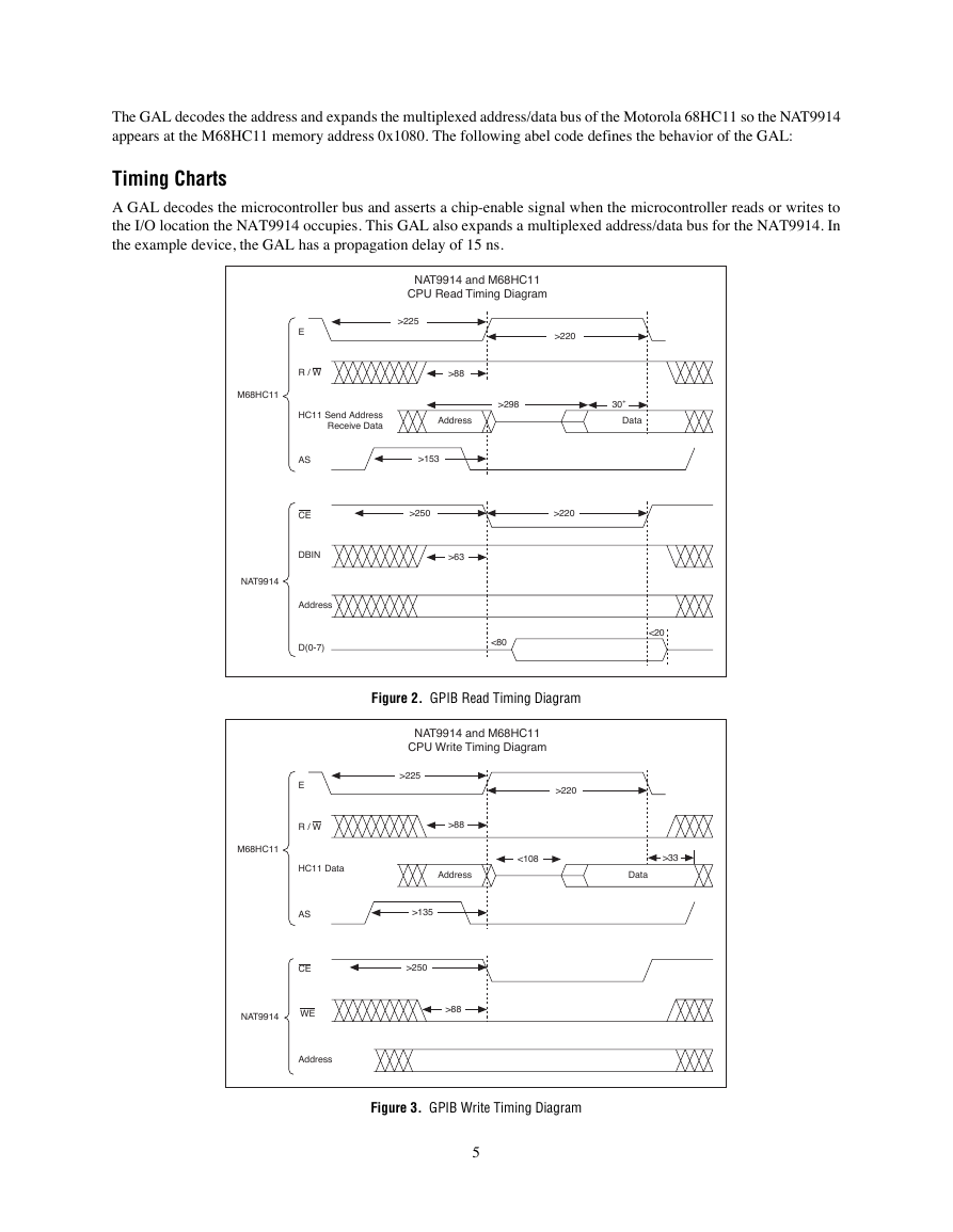
Timing Charts
A GAL decodes the microcontroller bus and asserts a chip-enable signal when the microcontroller reads or writes to
the I/O location the NAT9914 occupies. This GAL also expands a multiplexed address/data bus for the NAT9914. In
the example device, the GAL has a propagation delay of 15 ns.
NAT9914 and M68HC11
CPU Read Timing Diagram
>225
>220
>88
Address
>298
>153
30+
Data
>250
>220
>63
<80
<20
Figure 2. GPIB Read Timing Diagram
NAT9914 and M68HC11
CPU Write Timing Diagram
>225
>220
<108
>33
Data
>88
Address
>135
>250
E
R / W
M68HC11
HC11 Send Address
Receive Data
NAT9914
AS
CE
DBIN
Address
D(0-7)
E
R / W
M68HC11
HC11 Data
AS
CE
NAT9914
WE
>88
Address
Figure 3. GPIB Write Timing Diagram
5
�
Parts List
Part Description
Manufacturer
Part Number
GPIB interface chip
National Instruments
NAT9914APD
Address decoder
Lattice
GAL20V8B-15LP
GPIB transceivers
National Semiconductor
DS75160AN, DS75162AN
GPIB connector
2x30 Jumper block
Microcontroller
AMP
Samtec
Motorola
553121-1
TSW-130-07-S-D
M68HC11EVM
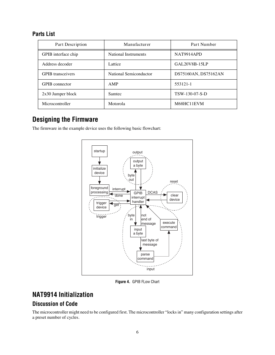
Designing the Firmware
The firmware in the example device uses the following basic flowchart:
startup
initialize
device
foreground
processing
trigger
device
trigger
output
output
a byte
byte
out
interrupt
done
get
DCAS
GPIB
interrupt
handler
reset
clear
device
byte
in
not
end of
message
input
a byte
execute
command
last byte of
message
parse
command
input
Figure 4. GPIB FLow Chart
NAT9914 Initialization
Discussion of Code
The microcontroller might need to be configured first. The microcontroller “locks in” many configuration settings after
a preset number of cycles.
6
�
The software must initialize the variables and interrupt vectors before the NAT9914 leaves the ‘pon’ mode. In the ‘pon’
mode, the NAT9914 logically disconnects from the GPIB and will not be affected by any GPIB activity.
The NAT9914 will become logically connected when the microcontroller sends the ‘~pon’ message to the NAT9914.
From this time on, the device will handle incoming GPIB signals.
The initialization of the microcontroller will depend greatly on the microcontroller you use, so the rest of this section
discusses initialization concerns of the NAT9914.
Clock Frequency
The NAT9914 uses the clock to generate the required IEEE 488.1 T1 delay between reading bytes. A faster clock
makes the delays more precise, but a 20 MHz clock runs the chip only slightly faster than a 5 MHz clock. You should
set the clock speed in the ICR register to indicate the external clock speed.
GPIB Address
The microcontroller must send the GPIB address of the device to the NAT9914 during the start-up initialization. Often
the user sets the GPIB address with DIP switches. Only 0 through decimal 30 are valid addresses. If a user enters 31,
a device usually interprets this as address 30.
End of Message Condition
The four methods of terminating a message are:
•
•
•
•
The listener stops listening after a certain number of bytes
The talker asserts the GPIB EOI signal
The talker sends an EOS byte (usually a newline character, hex 0A)
The talker sends the EOS with the EOI signal asserted
On the NAT9914, the XEOS bit in the ACCRA register configures the NAT9914 to assert EOI whenever the device
sends the character in EOSR to another GPIB device. The REOS bit of the same register sets the END bit of ISR0 if
the GPIB device receives an EOS character.
T1 Delay
The T1 delay is the time allowed for GPIB lines to settle before DAV asserts and gives the listening GPIB device
enough setup time to ensure reliable data transfer. The length of the delay depends on the capabilities of the
transceivers, GPIB cable length, and the number of powered-on GPIB devices. The stdl, ~stdl, vstdl, and ~vstdl
commands to the AUXCR register and the USTD bit in the ACCRI register set the IEEE 488.1 T1 delay. The
NAT9914 automatically shortens the delay after the first byte it sends. Internally, the NAT9914 uses the clock setting
to count out the T1 delay, so set the ICR register to indicate the clock speed.
Holdoff Condition When Listening
A GPIB device can refuse to accept a data byte or command byte until the device has processed the previous incoming
bytes. The device asserts the NDAC or NRFD lines and finishes processing the data before the device unasserts NDAC
or NRFD to continue the handshake. Most GPIB devices hold off the trigger and device-clear commands with an
NDAC holdoff. Some devices also perform a holdoff on the last byte in a message string and parse the message before
releasing the holdoff.
7
�
Detecting GPIB Events
GPIB events affecting the device are recorded in the ISR0, ISR1, and ISR2 registers. They give access to the current
GPIB status of the device and latch GPIB information for the microcontroller. The act of reading one of the ISR
registers also clears it. Firmware can either poll the ISR registers or ignore them until the NAT9914 interrupts.
Polling
One way to detect GPIB activity is to periodically poll the ISR registers. Most bits will not affect your device, but the
device firmware usually polls the BO, BI, END, GET, and DCAS bits. This method is straightforward and does not
have the overhead of interrupt calls.
Interrupts
The NAT9914 can be configured to interrupt when any enabled ISR bit sets. Note that by reading ISR0 bits INT0 and
INT1, your program may be able to handle the interrupt slightly faster. To configure interrupts for use on the
NAT9914, set the IMR bits corresponding to the ISR conditions which will request an interrupt. Then set the global
interrupt bit in IMR2.
In the example device, interrupt vector points to route_nat9914_interrupts() and a Return from Interrupt
instruction (RTI) replaces the Return from Subroutine instruction (RTS) at the end of route_nat9914_interrupts.
route_nat9914_interrupts() now sorts out what caused the interrupt and processes it completely before return-
ing microcontroller control back to the main program.
The NAT9914 INT* pin can be configured for active low or active high by setting or clearing the INV bit of the ACCRB
register. The INT* pin defaults to active low. The NAT9914 drives the INT* pin with an open collector gate, so wire
an external pullup resistor to it.
Parsing
The versatility of your device will specify the complexity of the parsing routine. This example device uses a simple
parsing algorithm. Both the buffer size and the parsing algorithm can easily be altered to accommodate more complex
command sets.
Reporting Device Status
The NAT9914 will return a status byte to the controller when the GPIB controller serial polls your device. The SPMR
register contains the status byte. The act of setting the RSV bit of the SPMR register asserts the SRQ line and requests
a serial poll. IEEE 488.2 defines the MAV bit, but leaves the lower nibble of the status byte device specific. The
NAT9914 handles serial polls without intervention by the microcontroller. This feature makes the status byte an ideal
place to keep status information and error messages.
Configure the SPMR through routines that strip away any writes to the RSV bit and replace writes to that particular bit
with calls to rsv2. In the example device, set_srq_bits() and clear_srq_bits() handle this function.
Some GPIB controllers automatically status poll devices and display the previous poll results instead of retrieving
newer status data. You may wish to disable auto serial polling when testing your device.
You can configure the NAT9914 with STBO IE in IMR2 to interrupt when the GPIB controller serial polls your device
and wait for the microcontroller to write a byte to the SPMR before the NAT9914 responds to the serial poll. For more
information on status reporting, refer to the NAT9914 Reference Manual.
8
�



 2023年江西萍乡中考道德与法治真题及答案.doc
 2012年重庆南川中考生物真题及答案.doc
 2013年江西师范大学地理学综合及文艺理论基础考研真题.doc
 2020年四川甘孜小升初语文真题及答案I卷.doc
 2020年注册岩土工程师专业基础考试真题及答案.doc
 2023-2024学年福建省厦门市九年级上学期数学月考试题及答案.doc
 2021-2022学年辽宁省沈阳市大东区九年级上学期语文期末试题及答案.doc
 2022-2023学年北京东城区初三第一学期物理期末试卷及答案.doc
 2018上半年江西教师资格初中地理学科知识与教学能力真题及答案.doc
 2012年河北国家公务员申论考试真题及答案-省级.doc
 2020-2021学年江苏省扬州市江都区邵樊片九年级上学期数学第一次质量检测试题及答案.doc
 2022下半年黑龙江教师资格证中学综合素质真题及答案.doc