SJA1105
5-port automotive Ethernet switch
Rev. 1 — 7 November 2016
Product data sheet
1. General description
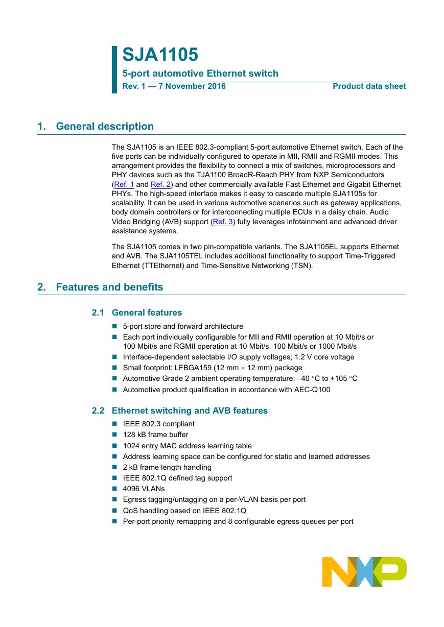
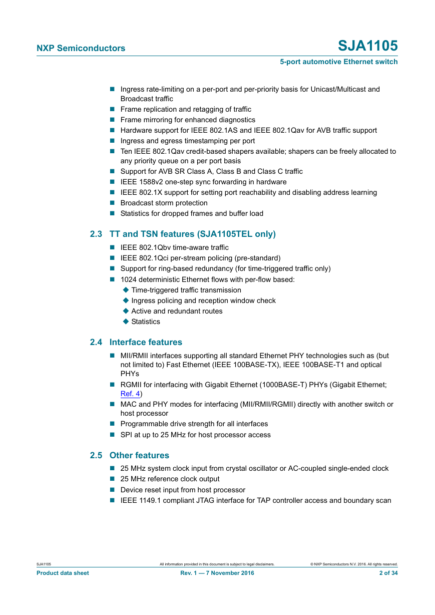
The SJA1105 is an IEEE 802.3-compliant 5-port automotive Ethernet switch. Each of the
five ports can be individually configured to operate in MII, RMII and RGMII modes. This
arrangement provides the flexibility to connect a mix of switches, microprocessors and
PHY devices such as the TJA1100 BroadR-Reach PHY from NXP Semiconductors
(Ref. 1 and Ref. 2) and other commercially available Fast Ethernet and Gigabit Ethernet
PHYs. The high-speed interface makes it easy to cascade multiple SJA1105s for
scalability. It can be used in various automotive scenarios such as gateway applications,
body domain controllers or for interconnecting multiple ECUs in a daisy chain. Audio
Video Bridging (AVB) support (Ref. 3) fully leverages infotainment and advanced driver
assistance systems.
The SJA1105 comes in two pin-compatible variants. The SJA1105EL supports Ethernet
and AVB. The SJA1105TEL includes additional functionality to support Time-Triggered
Ethernet (TTEthernet) and Time-Sensitive Networking (TSN).
2. Features and benefits
2.1 General features
5-port store and forward architecture
Each port individually configurable for MII and RMII operation at 10 Mbit/s or
100 Mbit/s and RGMII operation at 10 Mbit/s, 100 Mbit/s or 1000 Mbit/s
Interface-dependent selectable I/O supply voltages; 1.2 V core voltage
Small footprint: LFBGA159 (12 mm 12 mm) package
Automotive Grade 2 ambient operating temperature: 40 C to +105 C
Automotive product qualification in accordance with AEC-Q100
2.2 Ethernet switching and AVB features
IEEE 802.3 compliant
128 kB frame buffer
1024 entry MAC address learning table
Address learning space can be configured for static and learned addresses
2 kB frame length handling
IEEE 802.1Q defined tag support
4096 VLANs
Egress tagging/untagging on a per-VLAN basis per port
QoS handling based on IEEE 802.1Q
Per-port priority remapping and 8 configurable egress queues per port
�
NXP Semiconductors
SJA1105
5-port automotive Ethernet switch
Ingress rate-limiting on a per-port and per-priority basis for Unicast/Multicast and
Broadcast traffic
Frame replication and retagging of traffic
Frame mirroring for enhanced diagnostics
Hardware support for IEEE 802.1AS and IEEE 802.1Qav for AVB traffic support
Ingress and egress timestamping per port
Ten IEEE 802.1Qav credit-based shapers available; shapers can be freely allocated to
any priority queue on a per port basis
Support for AVB SR Class A, Class B and Class C traffic
IEEE 1588v2 one-step sync forwarding in hardware
IEEE 802.1X support for setting port reachability and disabling address learning
Broadcast storm protection
Statistics for dropped frames and buffer load
2.3 TT and TSN features (SJA1105TEL only)
IEEE 802.1Qbv time-aware traffic
IEEE 802.1Qci per-stream policing (pre-standard)
Support for ring-based redundancy (for time-triggered traffic only)
1024 deterministic Ethernet flows with per-flow based:
Time-triggered traffic transmission
Ingress policing and reception window check
Active and redundant routes
Statistics
2.4 Interface features
MII/RMII interfaces supporting all standard Ethernet PHY technologies such as (but
not limited to) Fast Ethernet (IEEE 100BASE-TX), IEEE 100BASE-T1 and optical
PHYs
RGMII for interfacing with Gigabit Ethernet (1000BASE-T) PHYs (Gigabit Ethernet;
Ref. 4)
MAC and PHY modes for interfacing (MII/RMII/RGMII) directly with another switch or
host processor
Programmable drive strength for all interfaces
SPI at up to 25 MHz for host processor access
2.5 Other features
25 MHz system clock input from crystal oscillator or AC-coupled single-ended clock
25 MHz reference clock output
Device reset input from host processor
IEEE 1149.1 compliant JTAG interface for TAP controller access and boundary scan
SJA1105
Product data sheet
All information provided in this document is subject to legal disclaimers.
Rev. 1 — 7 November 2016
© NXP Semiconductors N.V. 2016. All rights reserved.
2 of 34
�
NXP Semiconductors
3. Ordering information
SJA1105
5-port automotive Ethernet switch
Table 1.
Type number
SJA1105EL
SJA1105TEL
Ordering information
Package
Name
LFBGA159
Description
plastic low profile fine-pitch ball grid array package; 159 balls
Version
SOT1427-1
4. Block diagram
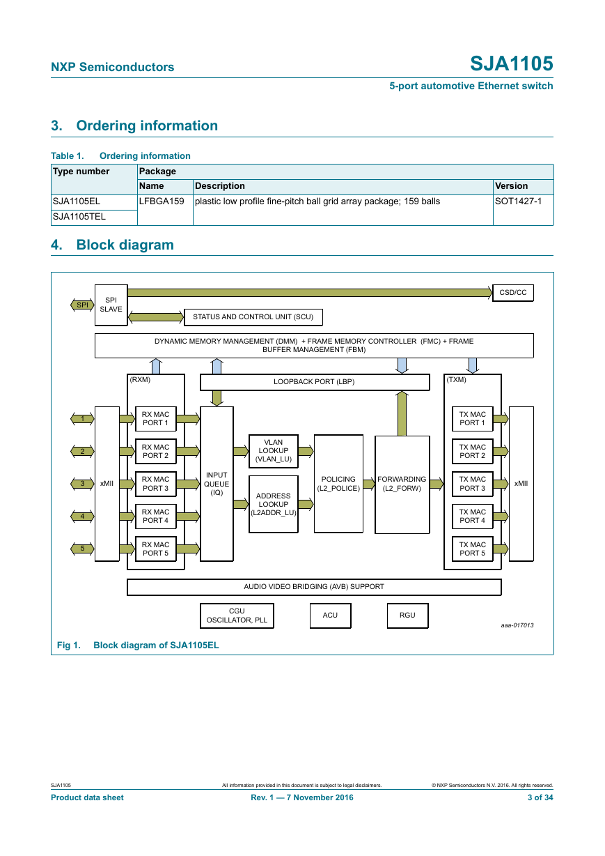
Fig 1. Block diagram of SJA1105EL
SJA1105
Product data sheet
All information provided in this document is subject to legal disclaimers.
Rev. 1 — 7 November 2016
© NXP Semiconductors N.V. 2016. All rights reserved.
3 of 34
�
NXP Semiconductors
SJA1105
5-port automotive Ethernet switch
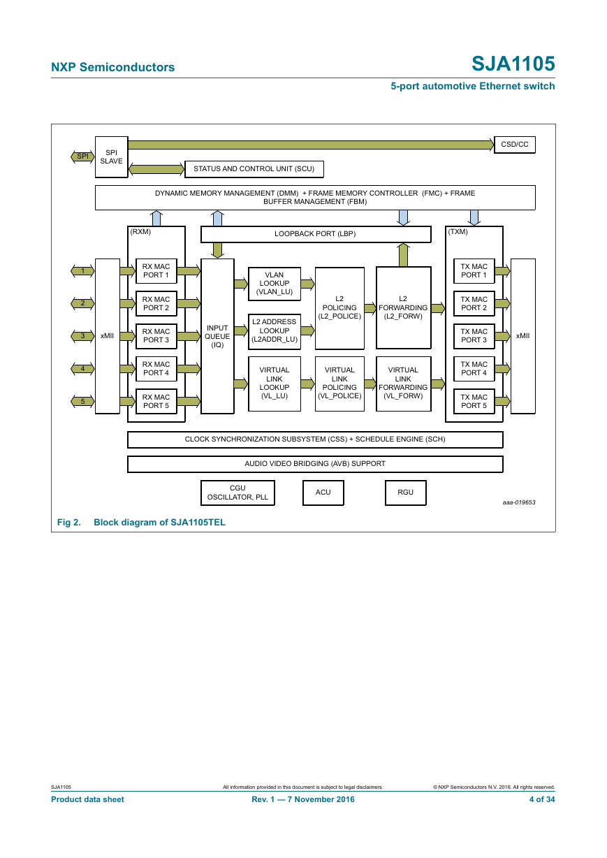
Fig 2. Block diagram of SJA1105TEL
SJA1105
Product data sheet
All information provided in this document is subject to legal disclaimers.
Rev. 1 — 7 November 2016
© NXP Semiconductors N.V. 2016. All rights reserved.
4 of 34
�
SJA1105
5-port automotive Ethernet switch
NXP Semiconductors
5. Pinning information
5.1 Pinning
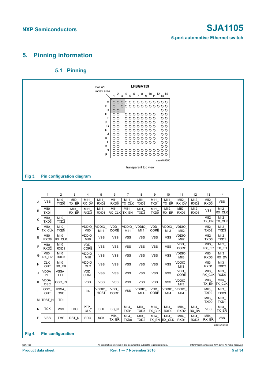
Fig 3.
Pin configuration diagram
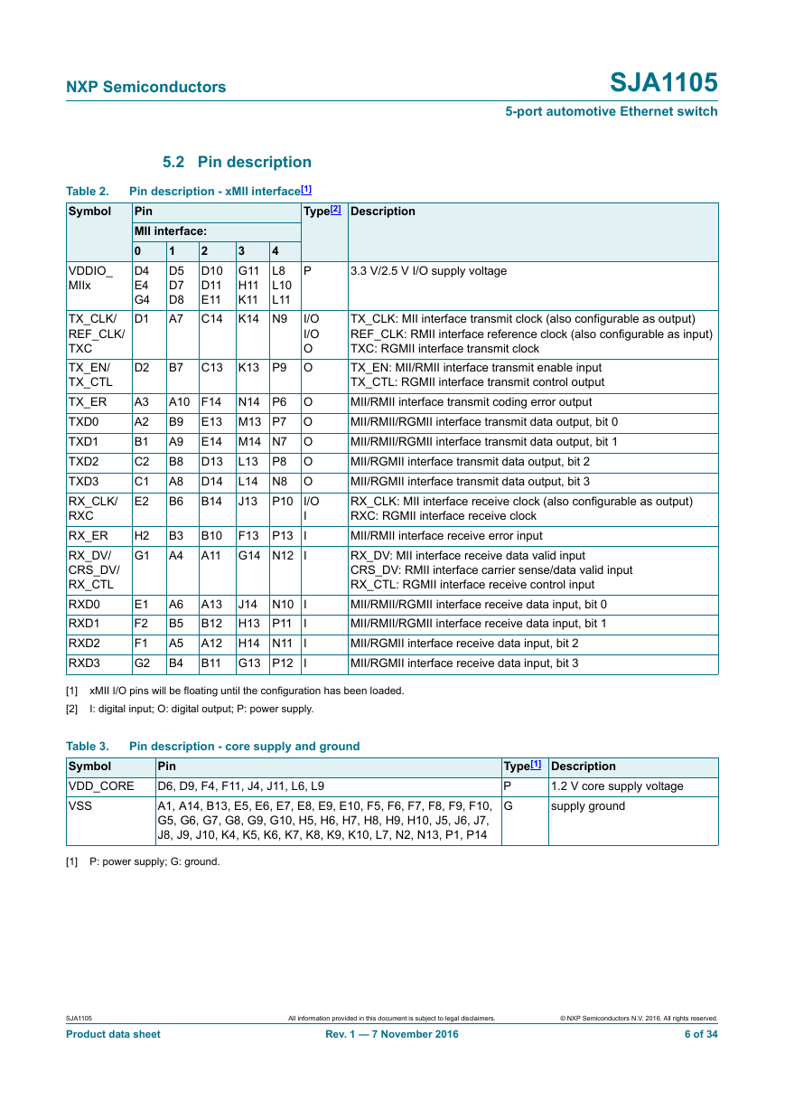
Fig 4.
Pin configuration
SJA1105
Product data sheet
All information provided in this document is subject to legal disclaimers.
Rev. 1 — 7 November 2016
© NXP Semiconductors N.V. 2016. All rights reserved.
5 of 34
�
NXP Semiconductors
SJA1105
5-port automotive Ethernet switch
Type[2] Description
3.3 V/2.5 V I/O supply voltage
TX_CLK: MII interface transmit clock (also configurable as output)
REF_CLK: RMII interface reference clock (also configurable as input)
TXC: RGMII interface transmit clock
TX_EN: MII/RMII interface transmit enable input
TX_CTL: RGMII interface transmit control output
MII/RMII interface transmit coding error output
MII/RMII/RGMII interface transmit data output, bit 0
MII/RMII/RGMII interface transmit data output, bit 1
MII/RGMII interface transmit data output, bit 2
MII/RGMII interface transmit data output, bit 3
RX_CLK: MII interface receive clock (also configurable as output)
RXC: RGMII interface receive clock
MII/RMII interface receive error input
RX_DV: MII interface receive data valid input
CRS_DV: RMII interface carrier sense/data valid input
RX_CTL: RGMII interface receive control input
MII/RMII/RGMII interface receive data input, bit 0
MII/RMII/RGMII interface receive data input, bit 1
MII/RGMII interface receive data input, bit 2
MII/RGMII interface receive data input, bit 3
5.2 Pin description
Pin description - xMII interface[1]
Pin
MII interface:
4
2
0
L8
D10
D4
L10
D11
E4
L11
G4
E11
C14 K14 N9
D1
3
G11
H11
K11
1
D5
D7
D8
A7
P
I/O
I/O
O
C13 K13 P9 O
B7
A10 F14 N14 P6 O
E13 M13 P7 O
B9
A9
E14 M14 N7 O
L13 P8 O
D13
B8
L14 N8 O
D14
A8
B6
B14
J13 P10 I/O
I
B10
F13 P13 I
A11 G14 N12 I
A13
J14 N10 I
B12 H13 P11 I
A12 H14 N11 I
B11 G13 P12 I
B3
A4
A6
B5
A5
B4
Table 2.
Symbol
VDDIO_
MIIx
TX_CLK/
REF_CLK/
TXC
TX_EN/
TX_CTL
TX_ER
TXD0
TXD1
TXD2
TXD3
RX_CLK/
RXC
RX_ER
RX_DV/
CRS_DV/
RX_CTL
RXD0
RXD1
RXD2
RXD3
D2
A3
A2
B1
C2
C1
E2
H2
G1
E1
F2
F1
G2
Table 3.
Symbol
VDD_CORE
VSS
[1]
[2]
xMII I/O pins will be floating until the configuration has been loaded.
I: digital input; O: digital output; P: power supply.
Pin description - core supply and ground
Pin
D6, D9, F4, F11, J4, J11, L6, L9
A1, A14, B13, E5, E6, E7, E8, E9, E10, F5, F6, F7, F8, F9, F10,
G5, G6, G7, G8, G9, G10, H5, H6, H7, H8, H9, H10, J5, J6, J7,
J8, J9, J10, K4, K5, K6, K7, K8, K9, K10, L7, N2, N13, P1, P14
Type[1] Description
P
G
1.2 V core supply voltage
supply ground
[1] P: power supply; G: ground.
SJA1105
Product data sheet
All information provided in this document is subject to legal disclaimers.
Rev. 1 — 7 November 2016
© NXP Semiconductors N.V. 2016. All rights reserved.
6 of 34
�
NXP Semiconductors
SJA1105
5-port automotive Ethernet switch
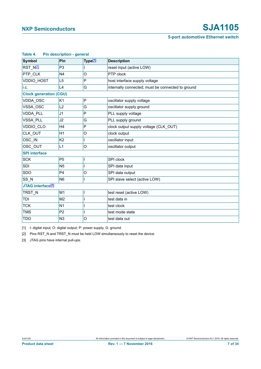
Pin description - general
Pin
P3
N4
L5
L4
K1
L2
J1
J2
H4
H1
K2
L1
Table 4.
Symbol
RST_N[2]
PTP_CLK
VDDIO_HOST
i.c.
Clock generation (CGU)
VDDA_OSC
VSSA_OSC
VDDA_PLL
VSSA_PLL
VDDIO_CLO
CLK_OUT
OSC_IN
OSC_OUT
SPI interface
SCK
SDI
SDO
SS_N
JTAG interface[3]
TRST_N
TDI
TCK
TMS
TDO
Type[1]
I
O
P
G
Description
reset input (active LOW)
PTP clock
host interface supply voltage
internally connected; must be connected to ground
P
G
P
G
P
O
I
O
I
I
O
I
I
I
I
I
O
oscillator supply voltage
oscillator supply ground
PLL supply voltage
PLL supply ground
clock output supply voltage (CLK_OUT)
clock output
oscillator input
oscillator output
SPI clock
SPI data input
SPI data output
SPI slave select (active LOW)
test reset (active LOW)
test data in
test clock
test mode state
test data out
P5
N5
P4
N6
M1
M2
N1
P2
N3
I: digital input; O: digital output; P: power supply, G: ground.
[1]
[2] Pins RST_N and TRST_N must be held LOW simultaneously to reset the device.
[3]
JTAG pins have internal pull-ups.
SJA1105
Product data sheet
All information provided in this document is subject to legal disclaimers.
Rev. 1 — 7 November 2016
© NXP Semiconductors N.V. 2016. All rights reserved.
7 of 34
�
NXP Semiconductors
6. Functional description
SJA1105
5-port automotive Ethernet switch
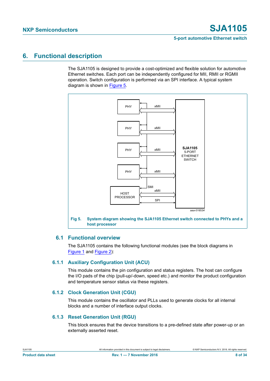
The SJA1105 is designed to provide a cost-optimized and flexible solution for automotive
Ethernet switches. Each port can be independently configured for MII, RMII or RGMII
operation. Switch configuration is performed via an SPI interface. A typical system
diagram is shown in Figure 5.
Fig 5.
System diagram showing the SJA1105 Ethernet switch connected to PHYs and a
host processor
6.1 Functional overview
The SJA1105 contains the following functional modules (see the block diagrams in
Figure 1 and Figure 2):
6.1.1 Auxiliary Configuration Unit (ACU)
This module contains the pin configuration and status registers. The host can configure
the I/O pads of the chip (pull-up/-down, speed etc.) and monitor the product configuration
and temperature sensor status via these registers.
6.1.2 Clock Generation Unit (CGU)
This module contains the oscillator and PLLs used to generate clocks for all internal
blocks and a number of interface output clocks.
6.1.3 Reset Generation Unit (RGU)
This block ensures that the device transitions to a pre-defined state after power-up or an
externally asserted reset.
SJA1105
Product data sheet
All information provided in this document is subject to legal disclaimers.
Rev. 1 — 7 November 2016
© NXP Semiconductors N.V. 2016. All rights reserved.
8 of 34
�


 2023年江西萍乡中考道德与法治真题及答案.doc
 2012年重庆南川中考生物真题及答案.doc
 2013年江西师范大学地理学综合及文艺理论基础考研真题.doc
 2020年四川甘孜小升初语文真题及答案I卷.doc
 2020年注册岩土工程师专业基础考试真题及答案.doc
 2023-2024学年福建省厦门市九年级上学期数学月考试题及答案.doc
 2021-2022学年辽宁省沈阳市大东区九年级上学期语文期末试题及答案.doc
 2022-2023学年北京东城区初三第一学期物理期末试卷及答案.doc
 2018上半年江西教师资格初中地理学科知识与教学能力真题及答案.doc
 2012年河北国家公务员申论考试真题及答案-省级.doc
 2020-2021学年江苏省扬州市江都区邵樊片九年级上学期数学第一次质量检测试题及答案.doc
 2022下半年黑龙江教师资格证中学综合素质真题及答案.doc