Part 1 - Input/Output Logical
Chapter 1 Overview
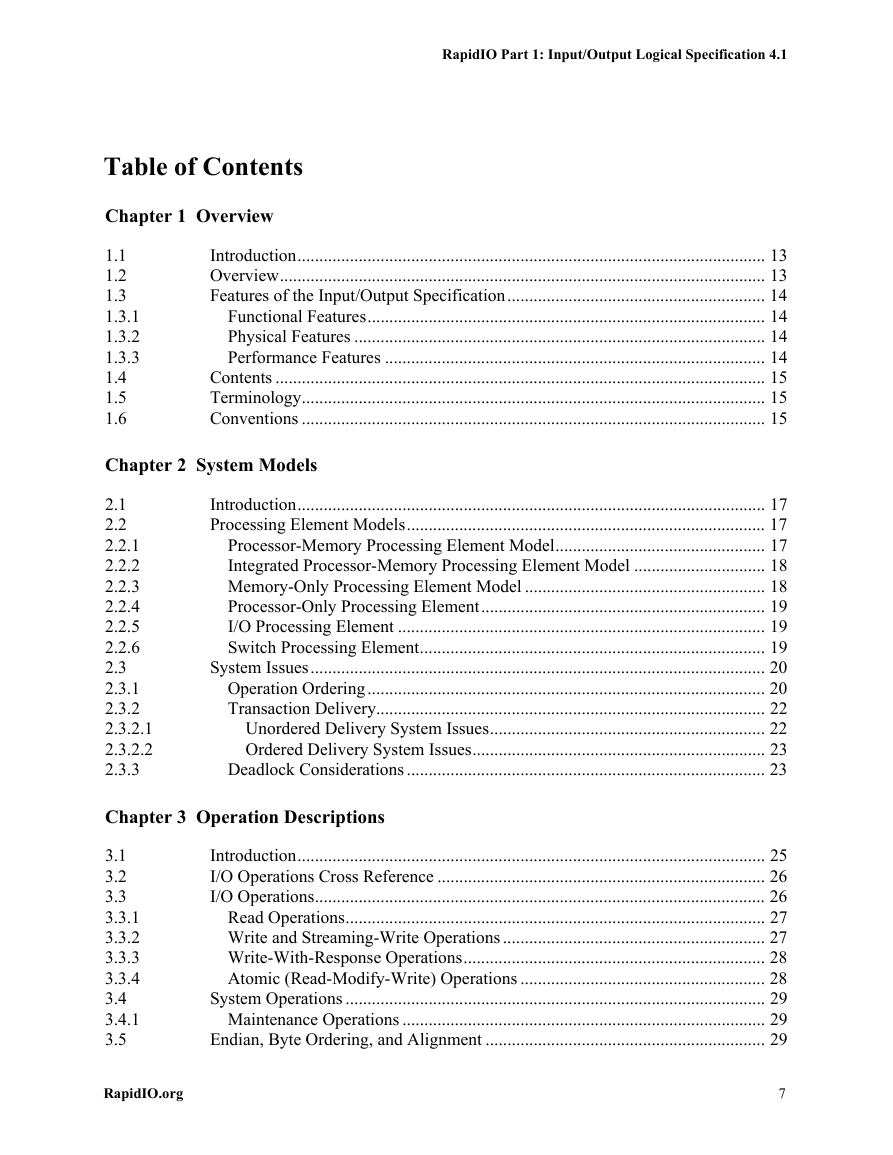
1.1 Introduction
1.2 Overview
1.3 Features of the Input/Output Specification
1.3.1 Functional Features
1.3.2 Physical Features
1.3.3 Performance Features
1.4 Contents
1.5 Terminology
1.6 Conventions
Chapter 2 System Models
2.1 Introduction
2.2 Processing Element Models
2.2.1 Processor-Memory Processing Element Model
2.2.2 Integrated Processor-Memory Processing Element Model
2.2.3 Memory-Only Processing Element Model
2.2.4 Processor-Only Processing Element
2.2.5 I/O Processing Element
2.2.6 Switch Processing Element
2.3 System Issues
2.3.1 Operation Ordering
2.3.2 Transaction Delivery
2.3.3 Deadlock Considerations
Chapter 3 Operation Descriptions
3.1 Introduction
3.2 I/O Operations Cross Reference
3.3 I/O Operations
3.3.1 Read Operations
3.3.2 Write and Streaming-Write Operations
3.3.3 Write-With-Response Operations
3.3.4 Atomic (Read-Modify-Write) Operations
3.4 System Operations
3.4.1 Maintenance Operations
3.5 Endian, Byte Ordering, and Alignment
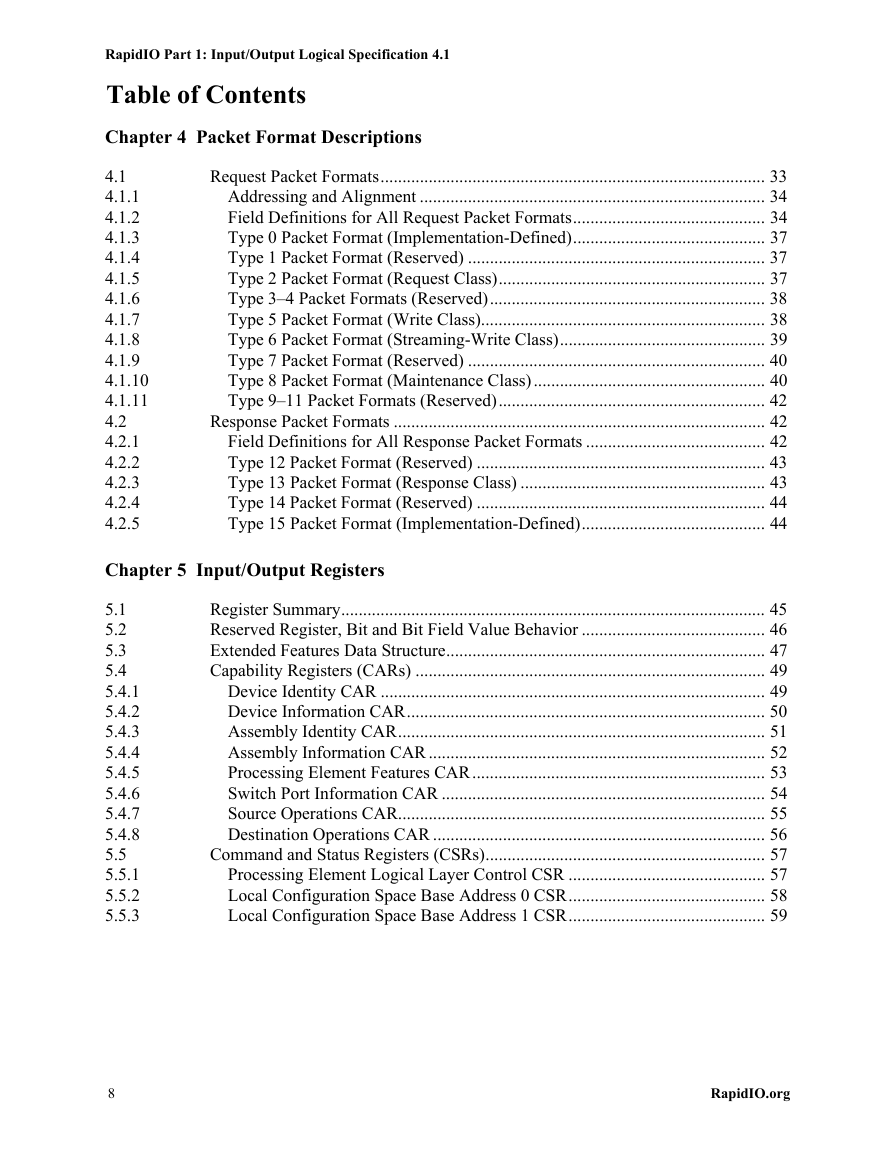
Chapter 4 Packet Format Descriptions
4.1 Request Packet Formats
4.1.1 Addressing and Alignment
4.1.2 Field Definitions for All Request Packet Formats
4.1.3 Type 0 Packet Format (Implementation-Defined)
4.1.4 Type 1 Packet Format (Reserved)
4.1.5 Type 2 Packet Format (Request Class)
4.1.6 Type 3–4 Packet Formats (Reserved)
4.1.7 Type 5 Packet Format (Write Class)
4.1.8 Type 6 Packet Format (Streaming-Write Class)
4.1.9 Type 7 Packet Format (Reserved)
4.1.10 Type 8 Packet Format (Maintenance Class)
4.1.11 Type 9–11 Packet Formats (Reserved)
4.2 Response Packet Formats
4.2.1 Field Definitions for All Response Packet Formats
4.2.2 Type 12 Packet Format (Reserved)
4.2.3 Type 13 Packet Format (Response Class)
4.2.4 Type 14 Packet Format (Reserved)
4.2.5 Type 15 Packet Format (Implementation-Defined)
Chapter 5 Input/Output Registers
5.1 Register Summary
5.2 Reserved Register, Bit and Bit Field Value Behavior
5.3 Extended Features Data Structure
5.4 Capability Registers (CARs)
5.4.1 Device Identity CAR
5.4.2 Device Information CAR
5.4.3 Assembly Identity CAR
5.4.4 Assembly Information CAR
5.4.5 Processing Element Features CAR
5.4.6 Switch Port Information CAR
5.4.7 Source Operations CAR
5.4.8 Destination Operations CAR
5.5 Command and Status Registers (CSRs)
5.5.1 Processing Element Logical Layer Control CSR
5.5.2 Local Configuration Space Base Address 0 CSR
5.5.3 Local Configuration Space Base Address 1 CSR
Part 2 - Message Passing Logical
Chapter 1 Overview
1.1 Introduction
1.2 Overview
1.3 Features of the Message Passing Specification
1.3.1 Functional Features
1.3.2 Physical Features
1.3.3 Performance Features
1.4 Contents
1.5 Terminology
1.6 Conventions
Chapter 2 System Models
2.1 Introduction
2.2 Processing Element Models
2.2.1 Processor-Memory Processing Element Model
2.2.2 Integrated Processor-Memory Processing Element Model
2.2.3 Memory-Only Processing Element Model
2.2.4 Processor-Only Processing Element
2.2.5 I/O Processing Element
2.2.6 Switch Processing Element
2.3 Message Passing System Model
2.3.1 Data Message Operations
2.3.2 Doorbell Message Operations
2.4 System Issues
2.4.1 Operation Ordering
2.4.2 Transaction Delivery
2.4.3 Deadlock Considerations
Chapter 3 Operation Descriptions
3.1 Introduction
3.2 Message Passing Operations Cross Reference
3.3 Message Passing Operations
3.3.1 Doorbell Operations
3.3.2 Data Message Operations
3.4 Endian, Byte Ordering, and Alignment
Chapter 4 Packet Format Descriptions
4.1 Introduction
4.2 Request Packet Formats
4.2.1 Field Definitions for All Request Packet Formats
4.2.2 Type 0 Packet Format (Implementation-Defined)
4.2.3 Type 1–9 Packet Formats (Reserved)
4.2.4 Type 10 Packet Formats (Doorbell Class)
4.2.5 Type 11 Packet Format (Message Class)
4.3 Response Packet Formats
4.3.1 Field Definitions for All Response Packet Formats
4.3.2 Type 12 Packet Format (Reserved)
4.3.3 Type 13 Packet Format (Response Class)
4.3.4 Type 14 Packet Format (Reserved)
4.3.5 Type 15 Packet Format (Implementation-Defined)
Chapter 5 Message Passing Registers
5.1 Introduction
5.2 Register Summary
5.3 Reserved Register, Bit and Bit Field Value Behavior
5.4 Capability Registers (CARs)
5.4.1 Source Operations CAR
5.4.2 Destination Operations CAR
5.5 Command and Status Registers (CSRs)
Annex A Message Passing Interface (Informative)
A.1 Introduction
A.2 Definitions and Goals
A.3 Message Operations
A.4 Inbound Mailbox Structure
A.4.1 Simple Inbox
A.4.2 Extended Inbox
A.4.3 Received Messages
A.5 Outbound Message Queue Structure
A.5.1 Simple Outbox
A.5.2 Extended Outbox
Part 3 - Common Transport
Chapter 1 Overview
1.1 Introduction
1.2 Overview
1.3 Transport Layer Features
1.3.1 Functional Features
1.3.2 Physical Features
1.3.3 Performance Features
1.4 Contents
1.5 Terminology
1.6 Conventions
Chapter 2 Transport Format Description
2.1 Introduction
2.2 System Topology
2.2.1 Switch-Based Systems
2.2.2 Ring-Based Systems
2.3 System Packet Routing
2.4 Field Alignment and Definition
2.5 Routing Maintenance Packets
Chapter 3 Common Transport Registers
3.1 Introduction
3.2 Register Summary
3.3 Reserved Register, Bit and Bit Field Value Behavior
3.4 Capability Registers (CARs)
3.4.1 Processing Element Features CAR
3.4.2 Switch Route Table Destination ID Limit CAR
3.5 Command and Status Registers (CSRs)
3.5.1 Base Device ID CSR
3.5.2 Dev32 Base Device ID CSR
3.5.3 Host Base Device ID Lock CSR
3.5.4 Component Tag CSR
3.5.5 Standard Route Cfg Destination ID Select CSR
3.5.6 Standard Route Cfg Port Select CSR
3.5.7 Standard Route Default Port CSR
3.6 Switch Routing Table Register Block
3.6.1 Register Map
3.6.2 Switch Routing Table Register Block Header
3.6.3 Broadcast Routing Table Control CSR
3.6.4 Broadcast Level 0 Info CSR
3.6.5 Broadcast Level 1 Info CSR
3.6.6 Broadcast Level 2 Info CSR
3.6.7 Port n Routing Table Control CSRs
3.6.8 Port n Level 0 Info CSRs
3.6.9 Port n Level 1 Info CSRs
3.6.10 Port n Level 2 Info CSRs
3.7 Routing Table Group Register Format
3.7.1 Broadcast Level 0 Group x Entry y Routing Table Entry CSR
3.7.2 Broadcast Level 1 Group x Entry y Routing Table Entry CSR
3.7.3 Broadcast Level 2 Group x Entry y Routing Table Entry CSR
3.7.4 Level 0 Group x Entry y Routing Table Entry CSR
3.7.5 Level 1 Group x Entry y Routing Table Entry CSR
3.7.6 Level 2 Group x Entry y Routing Table Entry CSR
Annex A Dev32 Hierarchical Programming Model (Informative)
A.1 Dev32 Configuration Examples
A.1.1 Example 1: Routing 0x00_11_20_** to Port 14
A.1.2 Example 2: Routing 0x00_11_0X_** to Port X
A.1.3 Example 3: Routing 0x00_ZZ_**_** to Port 15, ZZ=[0,0x10]
A.1.4 Example 4: All Other Packets Must Be Dropped
A.1.5 Example 5: Flat Routing Table Operation
Part 4 - Parallel Layer
Chapter 1 Overview
1.1 Introduction
1.2 Overview
1.3 Features of the Input/Output Specification
1.3.1 Functional features
1.3.2 Physical Features
1.3.3 Performance Features
1.4 Contents
1.5 Terminology
1.6 Conventions
Chapter 2 Physical Layer Protocol
2.1 Introduction
2.2 Packet Exchange Protocol
2.2.1 Packet and Control Alignment
2.2.2 Acknowledge Identification
2.3 Field Placement and Definition
2.3.1 Flow Control Fields Format
2.3.2 Packet Priority and Transaction Request Flows
2.3.3 Transaction and Packet Delivery
2.3.4 Resource Allocation
2.3.5 Flow Control Mode Negotiation
2.4 Error Detection and Recovery
2.4.1 Control Symbol Protection
2.4.2 Packet Protection
2.4.3 Lost Packet Detection
2.4.4 Implementation Note: Transactional Boundaries
2.4.5 Link Behavior Under Error
2.4.6 CRC Operation
2.4.7 CRC Code
2.5 Maximum Packet Size
2.6 Link Maintenance Protocol
2.6.1 Command Descriptions
2.6.2 Status Descriptions
Chapter 3 Packet and Control Symbol Transmission
3.1 Introduction
3.2 Packet Start and Control Symbol Delineation
3.3 Packet Termination
3.4 Packet Pacing
3.5 Embedded Control Symbols
3.6 Packet to Port Alignment
3.7 System Maintenance
3.7.1 Port and Link Initialization
3.7.2 Multicast-Event
3.8 Power Management
Chapter 4 Control Symbol Formats
4.1 Introduction
4.2 Acknowledgment Control Symbol Formats
4.2.1 Packet-Accepted Control Symbol
4.2.2 Packet-Retry Control Symbol
4.2.3 Packet-Not-Accepted Control Symbol
4.2.4 Canceling Packets
4.3 Packet Control Symbol Formats
4.4 Link Maintenance Control Symbol Formats
4.5 Reserved Symbol Formats
4.6 Implementation-defined Symbol Formats
4.7 Control Symbol to Port Alignment
Chapter 5 8/16 LP-LVDS Registers
5.1 Introduction
5.2 Register Map
5.3 Reserved Register, Bit and Bit Field Value Behavior
5.4 Capability Registers (CARs)
5.4.1 Processing Element Features CAR
5.5 Generic End Point Devices
5.5.1 Register Map
5.5.2 Command and Status Registers (CSRs)
5.6 Generic End Point Devices, software assisted error recovery option
5.6.1 Register Map
5.6.2 Command and Status Registers (CSRs)
5.7 Generic End Point Free Devices
5.7.1 Register Map
5.7.2 Command and Status Registers (CSRs)
5.8 Generic End Point Free Devices, software assisted error recovery option
5.8.1 Register Map
5.8.2 Command and Status Registers (CSRs)
Chapter 6 System Clocking Considerations
6.1 Introduction
6.2 Example Clock Distribution
6.3 Elasticity Mechanism
Chapter 7 Board Routing Guidelines
7.1 Introduction
7.2 Impedance
7.3 Skew
7.4 PCB Stackup
7.5 Termination
7.6 Additional Considerations
7.6.1 Single Board Environments
7.6.2 Single Connector Environments
7.6.3 Backplane Environments
7.7 Recommended pin escape ordering
Chapter 8 Signal Descriptions
8.1 Introduction
8.2 Signal Definitions
8.3 RapidIO Interface Diagrams
Chapter 9 Electrical Specifications
9.1 Introduction
9.2 Overview
9.3 DC Specifications
9.4 AC Specifications
9.4.1 Concepts and Definitions
9.4.2 Driver Specifications
9.4.3 Receiver Specifications
Annex A Interface Management (Informative)
A.1 Introduction
A.2 Link Initialization and Maintenance Mechanism
A.2.1 Input port training state machine
A.2.2 Output port training state machine
A.3 Packet Retry Mechanism
A.3.1 Input port retry recovery state machine
A.3.2 Output port retry recovery state machine
A.4 Error Recovery
A.4.1 Input port error recovery state machine
A.4.2 Output port error recovery state machine
Part 5 - GSM Logical
Chapter 1 Overview
1.1 Introduction
1.2 Overview
1.2.1 Memory System
1.3 Features of the Globally Shared Memory Specification
1.3.1 Functional Features
1.3.2 Physical Features
1.3.3 Performance Features
1.4 Contents
1.5 Terminology
1.6 Conventions
Chapter 2 System Models
2.1 Introduction
2.2 Processing Element Models
2.2.1 Processor-Memory Processing Element Model
2.2.2 Integrated Processor-Memory Processing Element Model
2.2.3 Memory-Only Processing Element Model
2.2.4 Processor-Only Processing Element
2.2.5 I/O Processing Element
2.2.6 Switch Processing Element
2.3 Programming Models
2.3.1 Globally Shared Memory System Model
2.4 System Issues
2.4.1 Operation Ordering
2.4.2 Transaction Delivery
2.4.3 Deadlock Considerations
Chapter 3 Operation Descriptions
3.1 Introduction
3.2 GSM Operations Cross Reference
3.3 GSM Operations
3.3.1 Read Operations
3.3.2 Instruction Read Operations
3.3.3 Read-for-Ownership Operations
3.3.4 Data Cache Invalidate Operations
3.3.5 Castout Operations
3.3.6 TLB Invalidate-Entry Operations
3.3.7 TLB Invalidate-Entry Synchronization Operations
3.3.8 Instruction Cache Invalidate Operations
3.3.9 Data Cache Flush Operations
3.3.10 I/O Read Operations
3.4 Endian, Byte Ordering, and Alignment
Chapter 4 Packet Format Descriptions
4.1 Introduction
4.2 Request Packet Formats
4.2.1 Addressing and Alignment
4.2.2 Data Payloads
4.2.3 Field Definitions for All Request Packet Formats
4.2.4 Type 0 Packet Format (Implementation-Defined)
4.2.5 Type 1 Packet Format (Intervention-Request Class)
4.2.6 Type 2 Packet Format (Request Class)
4.2.7 Type 3–4 Packet Formats (Reserved)
4.2.8 Type 5 Packet Format (Write Class)
4.2.9 Type 6–11 Packet Formats (Reserved)
4.3 Response Packet Formats
4.3.1 Field Definitions for All Response Packet Formats
4.3.2 Type 12 Packet Format (Reserved)
4.3.3 Type 13 Packet Format (Response Class)
4.3.4 Type 14 Packet Format (Reserved)
4.3.5 Type 15 Packet Format (Implementation-Defined)
Chapter 5 Globally Shared Memory Registers
5.1 Introduction
5.2 Register Summary
5.3 Reserved Register, Bit and Bit Field Value Behavior
5.4 Capability Registers (CARs)
5.4.1 Source Operations CAR
5.4.2 Destination Operations CAR
5.5 Command and Status Registers (CSRs)
Chapter 6 Communication Protocols
6.1 Introduction
6.2 Definitions
6.2.1 General Definitions
6.2.2 Request and Response Definitions
6.3 Operation to Protocol Cross Reference
6.4 Read Operations
6.4.1 Internal Request State Machine
6.4.2 Response State Machine
6.4.3 External Request State Machine
6.5 Instruction Read Operations
6.5.1 Internal Request State Machine
6.5.2 Response State Machine
6.5.3 External Request State Machine
6.6 Read for Ownership Operations
6.6.1 Internal Request State Machine
6.6.2 Response State Machine
6.6.3 External Request State Machine
6.7 Data Cache and Instruction Cache Invalidate Operations
6.7.1 Internal Request State Machine
6.7.2 Response State Machine
6.7.3 External Request State Machine
6.8 Castout Operations
6.8.1 Internal Request State Machine
6.8.2 Response State Machine
6.8.3 External Request State Machine
6.9 TLB Invalidate Entry, TLB Invalidate Entry Synchronize Operations
6.9.1 Internal Request State Machine
6.9.2 Response State Machine
6.9.3 External Request State Machine
6.10 Data Cache Flush Operations
6.10.1 Internal Request State Machine
6.10.2 Response State Machine
6.10.3 External Request State Machine
6.11 I/O Read Operations
6.11.1 Internal Request State Machine
6.11.2 Response State Machine
6.11.3 External Request State Machine
Chapter 7 Address Collision Resolution Tables
7.1 Introduction
7.2 Resolving an Outstanding READ_HOME Transaction
7.3 Resolving an Outstanding IREAD_HOME Transaction
7.4 Resolving an Outstanding READ_OWNER Transaction
7.5 Resolving an Outstanding READ_TO_OWN_HOME Transaction
7.6 Resolving an Outstanding READ_TO_OWN_OWNER Transaction
7.7 Resolving an Outstanding DKILL_HOME Transaction
7.8 Resolving an Outstanding DKILL_SHARER Transaction
7.9 Resolving an Outstanding IKILL_HOME Transaction
7.10 Resolving an Outstanding IKILL_SHARER Transaction
7.11 Resolving an Outstanding CASTOUT Transaction
7.12 Resolving an Outstanding TLBIE or TLBSYNC Transaction
7.13 Resolving an Outstanding FLUSH Transaction
7.14 Resolving an Outstanding IO_READ_HOME Transaction
7.15 Resolving an Outstanding IO_READ_OWNER Transaction
Part 6 - LP-Serial Physical
Chapter 1 Overview
1.1 Introduction
1.2 Contents
1.3 Terminology
1.4 Conventions
Chapter 2 Packets
2.1 Introduction
2.2 Packet Field Definitions
2.3 Packet Format
2.4 Packet Protection
2.4.1 Packet CRC Operation
2.4.2 CRC-16 Code
2.5 Maximum Packet Size
Chapter 3 Control Symbols
3.1 Introduction
3.2 Control Symbol Field Definitions
3.3 Control Symbol Format
3.4 Stype0 Control Symbols
3.4.1 Packet-Accepted Control Symbol
3.4.2 Packet-Retry Control Symbol
3.4.3 Packet-Not-Accepted Control Symbol
3.4.4 Timestamp Control Symbol
3.4.5 Status Control Symbol
3.4.6 VC-Status Control Symbol
3.4.7 Link-Response Control Symbol
3.4.8 Loop-Response Control Symbol
3.5 Stype1 Control Symbols
3.5.1 Start-of-Packet Control Symbol
3.5.2 Stomp Control Symbol
3.5.3 End-of-Packet Control Symbol
3.5.4 Restart-From-Retry Control Symbol
3.5.5 Link-Request Control Symbol
3.5.6 Timing Control Symbols
3.6 Control Symbol Protection
3.6.1 CRC-5 Code
3.6.2 CRC-5 Parallel Code Generation
3.6.3 CRC-13 Code
3.6.4 CRC-13 Parallel Code Generation
3.6.5 CRC-24 Code
3.6.6 CRC-24 Parallel Code Generation
Chapter 4 8b/10b PCS and PMA Layers
4.1 Introduction
4.2 PCS Layer Functions
4.3 PMA Layer Functions
4.4 Definitions
4.5 8b/10b Transmission Code
4.5.1 Character and Code-Group Notation
4.5.2 Running Disparity
4.5.3 Running Disparity Rules
4.5.4 8b/10b Encoding
4.5.5 Transmission Order
4.5.6 8b/10b Decoding
4.5.7 Special Characters and Columns
4.5.8 Effect of Single Bit Code-Group Errors
4.6 LP-Serial Link Widths
4.7 Idle Sequence
4.7.1 Clock Compensation Sequence
4.7.2 Idle Sequence 1 (IDLE1)
4.7.3 Idle Sequence 1 Generation
4.7.4 Idle Sequence 2 (IDLE2)
4.7.5 Idle Sequence Selection
4.8 Scrambling
4.8.1 Scrambling Rules
4.8.2 Descrambler Synchronization
4.8.3 Descrambler Synchronization Verification
4.9 1x Mode Transmission Rules
4.9.1 1x Ports
4.9.2 Nx Ports Operating in 1x Mode
4.10 Nx Link Striping and Transmission Rules
4.11 Retimers and Repeaters
4.11.1 Retimers
4.11.2 Repeaters
4.12 Port Initialization
4.12.1 1x Mode Initialization
4.12.2 1x/Nx Mode Initialization
4.12.3 Baud Rate Discovery
4.12.4 State Machines
4.13 Structurally Asymmetric Links
4.13.1 Definitions
4.13.2 Structurally Asymmetric Link Operation
4.14 Pseudo Random Binary Sequence Testing
Chapter 5 64b/67b PCS and PMA Layers
5.1 Introduction
5.2 PCS Layer Functions
5.3 PMA Layer Functions
5.4 Definitions
5.5 64b/67b Transmission Code
5.5.1 Codeword Format
5.5.2 Data Codeword
5.5.3 Control Codeword
5.5.4 Scrambling
5.5.5 Selective Codeword Inversion
5.5.6 Lane Check Calculation
5.5.7 Transmission Order
5.6 Packet Transmission Rules
5.6.1 Link CRC-32 Code
5.7 Packet Delimiting and Alignment
5.7.1 Packet Start Delimiter
5.7.2 Packet Termination Delimiters
5.8 Control Symbol Transmission Rules
5.9 Ordered Sequences
5.9.1 Seed Ordered Sequence
5.9.2 Status/Control Ordered Sequence
5.9.3 Skip Ordered Sequence
5.10 Idle Sequence
5.10.1 Idle Sequence 3 (IDLE3)
5.10.2 Idle Sequence 3 Generation
5.10.3 IDLE3 Idle Sequence Selection
5.11 Adaptive Equalization
5.11.1 Lane Training/Retraining
5.11.2 Ports Operating at 10.3125 and 12.5 Gbaud
5.11.3 Ports Operating at 25.78125 Gbaud
5.12 LP-Serial Link Widths
5.13 Transmission Rules
5.13.1 Order of Operation
5.13.2 1x Ports
5.13.3 Nx Ports Operating in 1x Mode
5.13.4 Kx Link Striping and Transmission Rules
5.14 Effect of Transmission Errors and Error Detection
5.15 Retimers and Repeaters
5.15.1 Retimers
5.15.2 Repeaters
5.16 Port Initialization
5.16.1 1x Mode Initialization
5.16.2 1x/Nx Mode Initialization
5.16.3 Baud Rate Discovery
5.17 Asymmetric Operation
5.17.1 Port Transmission Width
5.17.2 Port Receive Width
5.18 Structurally Asymmetric Links
5.19 State Machines
5.19.1 State Machine Conventions, Functions and Variables
5.19.2 Frame_Lock State Machine
5.19.3 Lane Training State Machines
5.19.4 Codeword Lock State Machine
5.19.5 Lane Synchronization State Machine
5.19.6 Lane Alignment State Machine
5.19.7 Port Initialization State Machine
5.19.8 Retrain/Transmit_Width_Control State Machine
5.19.9 Transmit Width State Machines
5.19.10 Receive Width State Machines
5.20 Pseudo Random Binary Sequence Testing
Chapter 6 LP-Serial Protocol
6.1 Introduction
6.2 Packet Exchange Protocol
6.3 Traffic types
6.4 Virtual Channels
6.4.1 Virtual channel 0 (VC0)
6.4.2 Virtual Channels 1-8 (VC1-8)
6.4.3 Virtual Channel Utilization
6.5 Control Symbols
6.5.1 Control Symbol Selection
6.5.2 Control Symbol Delimiting
6.5.3 Control Symbol Use
6.6 Packets
6.6.1 Packet Delimiting
6.6.2 Acknowledgment Identifier
6.6.3 Packet Priority and Transaction Request Flows
6.7 Link Maintenance Protocol
6.8 Packet Transmission Protocol
6.9 Flow Control
6.9.1 Receiver-Controlled Flow Control
6.9.2 Transmitter-Controlled Flow Control
6.9.3 Flow Control Mode Negotiation
6.10 Canceling Packets
6.11 Transaction and Packet Delivery Ordering Rules
6.12 Deadlock Avoidance
6.13 Error Detection and Recovery for Reliable Transmission
6.13.1 Lost Packet Detection
6.13.2 Link Behavior Under Error
6.14 Error Detection and Recovery for Error Free Mode Link Operation
6.15 Power Management
Chapter 7 LP-Serial Registers
7.1 Introduction
7.2 Register Map
7.3 Reserved Register, Bit and Bit Field Value Behavior
7.4 Capability Registers (CARs)
7.4.1 Processing Element Features CAR
7.5 LP-Serial Extended Feature Blocks
7.5.1 Generic Endpoint Devices
7.5.2 Generic Endpoint Devices, Software-assisted Error Recovery Option
7.5.3 Generic Endpoint Free Devices
7.5.4 Generic Endpoint Free Devices, Software-assisted Error Recovery Option
7.5.5 Register Map - I
7.5.6 Register Map - II
7.6 LP-Serial Command and Status Registers (CSRs)
7.6.1 LP-Serial Register Block Header
7.6.2 Port Link Timeout Control CSR
7.6.3 Port Response Timeout Control CSR
7.6.4 Port General Control CSR
7.6.5 Port n Link Maintenance Request CSRs
7.6.6 Port n Link Maintenance Response CSRs
7.6.7 Port n Local ackID CSRs
7.6.8 Port n Initialization Status CSRs
7.6.9 Port n Control 2 CSRs
7.6.10 Port n Error and Status CSRs
7.6.11 Port n Control CSRs
7.6.12 Port n Outbound ackID CSRs
7.6.13 Port n Inbound ackID CSRs
7.6.14 Port n Power Management CSRs
7.6.15 Port n Latency Optimization CSRs
7.6.16 Port n Link Timers Control CSRs
7.6.17 Port n Link Timers Control 2 CSRs
7.6.18 Port n Link Timers Control 3 CSRs
7.7 LP-Serial Lane Extended Features Block
7.7.1 Register Map
7.7.2 LP-Serial Lane Command and Status Registers (CSRs)
7.8 Virtual Channel Extended Features Block
7.8.1 Register Map
7.8.2 Virtual Channel Control Block Registers
7.9 Timestamp Generation Extension Block
7.9.1 Timestamp Generation Extension Block Header
7.9.2 Timestamp CAR
7.9.3 Timestamp Generator Status CSR
7.9.4 MECS Tick Interval CSR
7.9.5 MECS Next Timestamp MSW CSR
7.9.6 MECS Next Timestamp LSW CSR
7.9.7 Timestamp Generator MSW CSR
7.9.8 Timestamp Generator LSW CSR
7.9.9 Port n Timestamp 0 MSW CSRs
7.9.10 Port n Timestamp 0 LSW CSRs
7.9.11 Port n Timestamp 1 MSW CSRs
7.9.12 Port n Timestamp 1 LSW CSRs
7.9.13 Port n Timestamp Generator Synchronization CSRs
7.9.14 Port n Auto Update Counter CSRs
7.9.15 Port n Timestamp Synchronization Command CSRs
7.9.16 Port n Timestamp Synchronization Status CSRs
7.9.17 Port n Timestamp Offset CSRs
7.10 Miscellaneous Physical Layer Extension Block
7.10.1 Miscellaneous Physical Layer Extension Block Header
7.10.2 Miscellaneous Physical Layer CAR
7.10.3 Port n Reinit Control CSR
7.10.4 Port n SAL Control and Status CSR
7.10.5 Port n SMECS Control CSR
7.10.6 Port n PRBS Control CSR
7.10.7 Port n PRBS Lane Control CSR
7.10.8 Port n PRBS Status 0 CSR
7.10.9 Port n PRBS Status 1 CSR
7.10.10 Port n PRBS Locked Time CSR
7.10.11 Port n PRBS Seed CSR
Chapter 8 Signal Descriptions
8.1 Introduction
8.2 Signal Definitions
8.3 Serial RapidIO Interface Diagrams
Chapter 9 Common Electrical Specifications for less than 6.5 Gbaud LP-Serial Links
9.1 Introduction
9.2 References
9.3 Abbreviations
9.4 Definitions
9.4.1 Definition of Amplitude and Swing
9.4.2 Transmitter (Near-End) Template
9.4.3 Receiver (Far-End) Template
9.4.4 Definition of Skew and Relative Wander
9.4.5 Total Wander Mask
9.4.6 Relative Wander Mask
9.4.7 Random Jitter Mask
9.4.8 Defined Test Patterns
9.4.9 Reference Model
9.5 Common Electrical Specification
9.5.1 Introduction
9.5.2 Data Patterns
9.5.3 Signal Levels
9.5.4 Bit Error Ratio
9.5.5 Ground Differences
9.5.6 Cross Talk
9.5.7 Transmitter Test Load
9.5.8 Transmitter Lane-to-Lane Skew
9.5.9 Receiver Input Lane-to-Lane Skew
9.5.10 Transmitter Short Circuit Current
9.5.11 Differential Resistance and Return Loss, Transmitter and Receiver
9.5.12 Baud Rate Tolerance
9.5.13 Termination and DC Blocking
9.6 Pulse Response Channel Modelling
9.6.1 Generating a Pulse Response
9.6.2 Basic Pulse Response Definitions
9.6.3 Transmitter Pulse Definition
9.6.4 Receiver Pulse Response
9.6.5 Crosstalk Pulse Response
9.6.6 Decision Feedback Equalizer
9.6.7 Time Continuous Transverse Filter
9.6.8 Time Continuous Zero/Pole
9.6.9 Degrees of Freedom
9.7 Jitter Modelling
9.7.1 High Frequency Jitter vs. Wander
9.7.2 Total Wander vs. Relative Wander
9.7.3 Correlated vs. Uncorrelated Jitter
9.7.4 Jitter Distributions
9.7.5 Statistical Eye Methodology
Chapter 10 1.25 Gbaud, 2.5 Gbaud, and 3.125 Gbaud LP-Serial Links
10.1 Level I Application Goals
10.2 Equalization
10.3 Explanatory Note on Level I Transmitter and Receiver Specifications
10.4 Level I Electrical Specification
10.4.1 Level I Short Run Transmitter Characteristics
10.4.2 Level I Long Run Transmitter Characteristics
10.4.3 Level I Receiver Specifications
10.5 Level I Measurement and Test Requirements
10.5.1 Level I Transmitter Measurements
10.5.2 Level I Receiver Jitter Tolerance
Chapter 11 5 Gbaud and 6.25 Gbaud LP-Serial Links
11.1 Level II Application Goals
11.1.1 Common to Level II Short run, Medium run and Long run
11.1.2 Application Goals for Level II Short Run
11.1.3 Application Goals for Level II Medium Run
11.1.4 Application Goals for Long Run
11.1.5 Explanatory Note on Transmitter and Receiver Specifications
11.2 Equalization
11.3 Link Compliance Methodology
11.3.1 Overview
11.3.2 Reference Models
11.3.3 Channel Compliance
11.3.4 Transmitter Compliance
11.3.5 Receiver Compliance
11.4 Level II Short Run Interface - General Requirements
11.4.1 Jitter and Inter-operability Methodology
11.4.2 Level II SR Electrical Characteristics
11.4.3 Level II SR StatEye.org Template
11.5 Level II Long Run Interface General Requirements
11.5.1 Long Run Jitter and Inter-operability Methodology
11.5.2 Level II LR Interface Electrical Characteristics
11.5.3 Level II LR Link and Jitter Budgets
11.5.4 Level II LR StatEye.org Template
11.6 Level II Medium Run Interface General Requirements
11.6.1 Medium Run Jitter and Inter-operability Methodology
11.6.2 Level II MR Interface Electrical Characteristics
11.6.3 Level II MR Link and Jitter Budgets
11.6.4 Level II MR StatEye.org Template
11.7 Level II Measurement and Test Requirements
11.7.1 High Frequency Transmit Jitter Measurement
11.7.2 Total Transmit Wander Measurement
11.7.3 Relative Transmit Wander Measurement
11.7.4 Jitter Tolerance
Chapter 12 Electrical Specification for 10.3125 and 12.5 Gbaud LP-Serial Links
12.1 References
12.2 Level III Application Requirements
12.2.1 Common to Level III Short-reach and Long-reach
12.2.2 Application Requirements for Level III Short-reach
12.2.3 Application Requirements for Level III Long-reach
12.3 Equalization
12.3.1 Receiver
12.3.2 Transmitter
12.4 Level III Electrical Specification
12.4.1 Level III Short-reach
12.4.2 Level III Long-reach
12.4.3 Level III Transmitter Lane-to-Lane Skew
12.4.4 Receiver Input Lane-to-Lane Skew
12.4.5 Electrical IDLE
Chapter 13 Electrical Specification for 25 Gbaud LP-Serial Links
13.1 References
13.2 Level IV Application Requirements
13.2.1 Common to Level IV Short-reach and Long-reach
13.2.2 Application Requirements for Level IV Short-reach
13.2.3 Application Requirements for Level IV Long-reach
13.3 Equalization
13.3.1 Receiver
13.3.2 Transmitter
13.4 Level IV Electrical Specification
13.4.1 Level IV Short-reach
13.4.2 Level IV Long-reach
13.4.3 Level IV Transmitter Lane-to-Lane Skew
13.4.4 Receiver Input Lane-to-Lane Skew
13.4.5 Electrical IDLE
Annex A Transmission Line Theory and Channel Information (Informative)
A.1 Transmission Lines Theory
A.2 Impedance Matching
A.3 Impedance Definition Details
A.4 Density considerations
A.5 Common-Mode Impedance and Return Loss
A.6 Crosstalk Considerations
A.7 Equation Based Channel Loss by Curve Fit
Annex B BER Adjustment Methodology (Informative)
B.1 Extrapolation of Correlated Bounded Gaussian Jitter to low BERs
B.1.1 Bathtub Measurements
B.2 Confidence Level of Errors Measurement
B.3 Eye Mask Adjustment for Sampling Oscilloscopes
B.3.1 Theory
B.3.2 Usage
Annex C Interface Management (Informative)
C.1 Introduction
C.2 Packet Retry Mechanism
C.2.1 Input port retry recovery state machine
C.2.2 Output port retry recovery state machine
C.3 Error Recovery
C.3.1 Input port error recovery state machine
C.3.2 Output port error recovery state machine
C.3.3 Changes in Error Recovery Behavior for CT
Annex D Critical Resource Performance Limits (Informative)
D.1 IDLE1 and IDLE2
D.2 IDLE3
Annex E Manufacturability and Testability (Informative)
Annex F Multiple Port Configuration Example (Informative)
F.1 Introduction
F.2 System with Different Port Width Capabilities
Annex G MECS Time Synchronization (Informative)
G.1 Introduction
G.2 Detection of Missing MECS
G.3 MECS and SMECS Redundant Operation
G.4 Detection of (S)MECS Source Failure
Part 7 - System and Device Interoperability
Chapter 1 Overview
1.1 Introduction
1.2 Overview
Chapter 2 System Exploration and Initialization
2.1 Introduction
2.2 Boot code access
2.3 Exploration and initialization
2.3.1 Exploration and initialization rules
2.3.2 Exploration and initialization algorithm
2.3.3 Exploration and initialization example
Chapter 3 RapidIO Device Class Requirements
3.1 Introduction
3.2 Class Partitioning
3.2.1 Generic: All devices
3.2.2 Class 1: Simple target device
3.2.3 Class 2: Simple mastering device
3.2.4 Class 3: Complex mastering device
3.3 HARSH Device Profiles
3.3.1 Basic HARSH Device Requirements
3.3.2 Enhanced HARSH Device Requirements
3.3.3 HARSH-10xN Device Requirements
3.3.4 HARSH Switch Device Requirements
3.3.5 HARSH Endpoint Device Requirements
3.3.6 HARSH Endpoint-E Device Requirements
Chapter 4 PCI Considerations
4.1 Introduction
4.2 Address Map Considerations
4.3 Transaction Flow
4.3.1 PCI 2.2 Transaction Flow
4.3.2 PCI-X Transaction Flow
4.4 RapidIO to PCI Transaction Mapping
4.5 Operation Ordering and Transaction Delivery
4.5.1 Operation Ordering
4.5.2 Transaction Delivery Ordering
4.5.3 PCI-X Relaxed Ordering Considerations
4.6 Interactions with Globally Shared Memory
4.6.1 I/O Read Operation Details
4.6.2 Data Cache Flush Operation Details
4.7 Byte Lane and Byte Enable Usage
4.8 Error Management
Chapter 5 Globally Shared Memory Devices
5.1 Introduction
5.2 Processing Element Behavior
5.2.1 Processor-Memory Processing Element
5.2.2 Memory-only Processing Element
5.2.3 Processor-only Processing Element
5.2.4 I/O Processing Element
5.2.5 Switch Processing Element
5.3 Transaction to Priority Mappings
Part 8 - Error Management-Hot Swap
Chapter 1 Error Management Extensions
1.1 Introduction
1.2 Physical Layer Extensions
1.2.1 Port n Error Detect, Enable, and Capture CSRs
1.2.2 Error Reporting Thresholds
1.2.3 Error Rate Control and Status
1.2.4 Port Behavior When Error Rate Failed Threshold is Reached
1.2.5 Packet Timeout Mechanism in a Switch Device
1.2.6 Hot Swap Extensions
1.2.7 Physical Layer Multiple Event Capture
1.3 Logical and Transport Layer Extensions
1.3.1 Logical/Transport Error Detect, Enable, and Capture CSRs
1.3.2 Message Passing Error Detection
1.3.3 Other Logical Layer Errors
1.3.4 Logical/Transport Layer Multiple Event Capture
1.4 System Software Notification of Error
1.5 Mechanisms for Software Debug
1.6 IDLE3 Port_Status Extension
Chapter 2 Error Management Registers
2.1 Introduction
2.2 Additions to Existing Registers
2.2.1 Port n Control CSRs
2.2.2 Port n Error and Status CSRs
2.3 New Error Management Registers
2.4 Register Map
2.5 Command and Status Registers (CSRs)
2.5.1 Error Management Extensions Block Header
2.5.2 Error Management/Hot Swap Extension Block CAR
2.5.3 Logical/Transport Layer Error Detect CSR
2.5.4 Logical/Transport Layer Error Enable CSR
2.5.5 Logical/Transport Layer High Address Capture CSR
2.5.6 Logical/Transport Layer Address Capture CSR
2.5.7 Logical/Transport Layer Device ID Capture CSR
2.5.8 Logical/Transport Layer Control Capture CSR
2.5.9 Logical/Transport Layer Dev32 Destination ID Capture CSR
2.5.10 Logical/Transport Layer Dev32 Source ID Capture CSR
2.5.11 Port-Write Target deviceID CSR
2.5.12 Packet Time-to-live CSR
2.5.13 Port-write Dev32 Target deviceID CSR
2.5.14 Port-Write Transmission Control CSR
2.5.15 Port n Error Detect CSR
2.5.16 Port n Error Rate Enable CSR
2.5.17 Port n Attributes Capture CSR
2.5.18 Port n Capture 0 CSR
2.5.19 Port n Capture 1 CSR
2.5.20 Port n Capture 2 CSR
2.5.21 Port n Capture 3 CSR
2.5.22 Port n Capture 4 CSR
2.5.23 Port n Error Rate CSR
2.5.24 Port n Error Rate Threshold CSR
2.5.25 Port n Link Uninit Discard Timer CSR
2.5.26 Port n FIFO Error Detect CSR
Annex A Error Management Discussion (Informative)
A.1 Introduction
A.2 Limitations of Error Management Discussion
A.3 Hot-insertion/extraction Discussion
A.4 Port-write Discussion
A.5 Physical Layer Fatal Error Recovery Discussion
Part 9 - Flow Control Logical
Chapter 1 Flow Control Overview
1.1 Congestion Management
1.1.1 Introduction
1.1.2 Requirements
1.1.3 Problem Illustration
1.2 Flow Arbitration
1.2.1 Fixed / Static Resource Allocation
1.2.2 Dynamic Resource Allocation Protocol
Chapter 2 Logical Layer Flow Control Operation
2.1 Fabric Link Congestion
2.2 Flow Arbitration
2.2.1 Arbitration Protocol
2.2.2 Number Of Outstanding Requests
2.3 Flow Control Operation
2.4 Physical Layer Requirements
2.4.1 Fabric Topology
2.4.2 Flow Control Transaction Transmission
2.4.3 Priority to Transaction Request Flow Mapping
2.4.4 Flow Control Transaction Ordering Rules
2.4.5 End Point Congestion Management Rules
2.4.6 Switch Congestion Management Rules
2.4.7 Endpoint Rules for the Arbitration Protocol
2.4.8 Abnormal De-allocation of Resources
Chapter 3 Packet Format Descriptions
3.1 Introduction
3.2 Logical Layer Packet Format
3.3 Flow Arbitration Message Fields (FAM)
3.4 Transport and Physical Layer Packet Format
Chapter 4 Logical Layer Flow Control Extensions Register Bits
4.1 Introduction
4.2 Capability Registers (CARs)
4.2.1 Processing Elements Features CAR
4.2.2 Port n Control CSR
Annex A Flow Control Examples (Informative)
A.1 Congestion Detection and Remediation
A.2 Orphaned XOFF Mechanism Description
A.3 Discussion on Flow Arbitration
Part 10 - Data Streaming Logical
Chapter 1 Overview
1.1 Introduction
1.2 Overview
1.3 Features of the Data Streaming Specification
1.3.1 Functional Features
1.3.2 Physical Features
1.3.3 Performance Features
1.4 Contents
1.5 Terminology
1.6 Conventions
1.7 Useful References
Chapter 2 Data Streaming Systems
2.1 Introduction
2.2 System Example
2.3 Traffic Streams
2.4 Operation Ordering
2.5 Class of Service and Virtual Queues
2.6 End-to-end Traffic Management
2.7 Deadlock Considerations
Chapter 3 Operation Descriptions
3.1 Introduction
3.2 Data Streaming Protocol
3.2.1 Data Streaming Operation
3.2.2 Virtual Streams
3.2.3 PDU Sequences Within Streams
3.2.4 Segments within a PDU
3.2.5 Rules for Segmentation and Reassembly
3.3 Class of Service and Traffic Streams
3.4 Traffic Management
3.4.1 Traffic Management Operand
3.4.2 On/Off Traffic Management
3.4.3 Rate Base Traffic Management
3.4.4 Credit Based Traffic Management
3.4.5 Rules for Traffic Management
Chapter 4 Packet Format Descriptions
4.1 Introduction
4.2 Type 9 Packet Format (Data-Streaming Class)
4.3 Type 9 Extended Packet Format
4.3.1 TM Operand
4.3.2 Basic Traffic Management
4.3.3 Rate Based Traffic Management
4.3.4 Credit Based Traffic Management
Chapter 5 Data Streaming Registers
5.1 Introduction
5.2 Register Summary
5.3 Reserved Register, Bit and Bit Field Value Behavior
5.4 Additions to Existing Registers
5.5 Capability Registers (CARs)
5.5.1 Source Operations CAR
5.5.2 Destination Operations CAR
5.5.3 Data Streaming Information CAR
5.6 Command and Status Registers (CSRs)
5.6.1 Data Streaming Logical Layer Control CSR
Annex A VSID Usage Examples
A.1 Introduction
A.2 Background
A.3 Packet Classification
A.3.1 Sub-port Addressing at the Destination
A.3.2 Virtual Output Queueing - Fabric On-ramp
A.4 System Requirements
A.4.1 UTOPIA to RapidIO ATM bridge
A.4.2 Network processor
A.4.3 CSIX to RapidIO interface
A.4.4 10Gb Metropolitan Area Network interface
Part 11 - Multicast Extensions
Chapter 1 Overview
1.1 Introduction
1.2 Overview
1.3 Requirements
Chapter 2 Multicast Extensions Behavior
2.1 Introduction
2.2 Packet Replication
2.3 Multicast Operation
2.4 Multicast Transaction Ordering Requirements
Chapter 3 Port Aggregation Extensions Behavior
3.1 Introduction
3.2 Port Aggregation Interoperability
3.3 Port Aggregation Operation
3.3.1 Fail-over Port Selection
3.4 Port Aggregation Transaction Ordering Requirements
Chapter 4 Multicast and Port Aggregation Extensions Registers
4.1 Introduction
4.2 Capability Registers (CARs)
4.2.1 Processing Elements Features CAR
4.2.2 Switch Multicast Support CAR
4.2.3 Switch Multicast Information CAR
4.3 Command and Status Registers (CSRs)
4.3.1 Multicast Mask Port CSR
4.3.2 Multicast Associate Select CSR
4.3.3 Multicast Associate Operation CSR
4.4 Switch Routing Table Register Block
4.4.1 Register Map
4.4.2 Broadcast Routing Table Control CSR
4.4.3 Broadcast Multicast Info CSR
4.4.4 Broadcast Port Aggregation Mask Info CSR
4.4.5 Port n Routing Table Control CSR
4.4.6 Port n Multicast Info CSR
4.4.7 Port n Port Aggregation Mask Info CSR
4.4.8 Broadcast Multicast Mask x Set Register y CSR
4.4.9 Broadcast Multicast Mask x Clear Register y CSR
4.4.10 Broadcast Port Aggregation Mask x Set Register y CSR
4.4.11 Broadcast Port Aggregation Mask x Clear Register y CSR
4.4.12 Broadcast Port Aggregation Mask x Control Register 0 CSR
4.4.13 Broadcast Port Aggregation Mask x Control Register y CSR
4.4.14 Port n Multicast Mask x Set Register y CSR
4.4.15 Port n Multicast Mask x Clear Register y CSR
4.4.16 Port n Port Aggregation Mask x Set Register y CSR
4.4.17 Port n Port Aggregation Mask x Clear Register y CSR
4.4.18 Port n Port Aggregation Mask x Control Register 0 CSR
4.4.19 Port n Port Aggregation Mask x Control Register y CSR
Chapter 5 Configuration Examples
5.1 Introduction
5.2 Configuring Multicast Masks
5.2.1 Clearing Multicast Masks
5.2.2 Assigning Ports to Multicast Masks
5.2.3 Removing a Port from a Multicast Mask
5.2.4 Querying a Multicast Mask
5.3 Simple Association
5.3.1 Restrictions on Block Size
5.3.2 Restrictions on Block Associate
5.3.3 Restrictions on Associations
5.4 Configuring Associations
5.4.1 Basic Association
5.4.2 Using Per-Ingress Port Association
5.4.3 Using Block Association
5.4.4 Using Per-Ingress Port and Block Association
5.4.5 Removing a Destination ID to Multicast Mask Association
5.4.6 Querying an Association
Annex A End Point Considerations (Informative)
A.1 Introduction
A.2 Multicast Destination ID
A.3 End Point Multicast Channels
Annex B Multicast Applications (Informative)
B.1 Introduction
B.2 Example 1 - Static Multicast Masks
B.3 Example 2 - Linking Multicast Masks to Destination IDs
Part 12 - VOQ Extensions
Chapter 1 Introduction
1.1 Problem Illustration 9
1.2 Terminology 10
1.3 Conventions 10
Chapter 2 Overview
2.1 Congestion Message 13
2.2 Traffic Staging 14
2.3 Adding Device Independence 15
2.4 Relationship With Virtual Channels 16
2.5 Additional Queueing Considerations 16
Chapter 3 Control Symbol Format
3.1 Stype2 Control Symbol 48 19
3.2 Control Symbol 64 VoQ Backpressure 20
3.3 VoQ Backpressure per VC 22
Chapter 4 Rules
4.1 Implementation Rules 23
4.2 Rules for Generating Backpressure Control Symbols 23
4.3 Rules for Interpreting Backpressure Control Symbols 24
Chapter 5 Register Definitions
5.1 VoQ Backpressure Extended Features Block 25
5.1.1 Register Map 25
5.1.2 VoQ Backpressure Control Block Registers 26
5.1.2.1 LP-Serial VC Register Block Header 26
5.1.2.2 Port n VoQ Control Status Register 27
Chapter 1 Introduction
1.1 Problem Illustration
1.2 Terminology
1.3 Conventions
Chapter 2 Overview
2.1 Congestion Message
2.2 Traffic Staging
2.3 Adding Device Independence
2.4 Relationship With Virtual Channels
2.5 Additional Queueing Considerations
Chapter 3 Control Symbol Format
3.1 Stype2 Control Symbol 48
3.2 Control Symbol 64 VoQ Backpressure
3.3 VoQ Backpressure per VC
Chapter 4 Rules
4.1 Implementation Rules
4.2 Rules for Generating Backpressure Control Symbols
4.3 Rules for Interpreting Backpressure Control Symbols
Chapter 5 Register Definitions
5.1 VoQ Backpressure Extended Features Block
5.1.1 Register Map
5.1.2 VoQ Backpressure Control Block Registers
Annex 1 - Software-System Bring Up
Chapter 1 Overview
1.1 Introduction
1.2 Overview
1.3 Scope
1.4 System Enumeration API
1.5 Terminology
1.6 Software Conventions
Chapter 2 Requirements for System Bring Up
2.1 Introduction
2.2 Boot Requirements
2.3 Enumeration Completion
2.4 Enumeration Time-Out
2.5 Function Return Codes
Chapter 3 Hardware Abstraction Layer
3.1 Introduction
3.2 Device Addressing
3.3 HAL Functions
3.3.1 Types and Definitions
3.3.2 rioGetNumLocalPorts
3.3.3 rioConfigurationRead
3.3.4 rioConfigurationWrite
Chapter 4 Standard Bring Up Functions
4.1 Introduction
4.2 Data Structures
4.3 Bring Up Functions
4.3.1 rioInitLib
4.3.2 rioGetFeatures
4.3.3 rioGetSwitchPortInfo
4.3.4 rioGetExtFeaturesPtr
4.3.5 rioGetNextExtFeaturesPtr
4.3.6 rioGetSourceOps
4.3.7 rioGetDestOps
4.3.8 rioGetAddressMode
4.3.9 rioGetBaseDeviceId
4.3.10 rioSetBaseDeviceId
4.3.11 rioAcquireDeviceLock
4.3.12 rioReleaseDeviceLock
4.3.13 rioGetComponentTag
4.3.14 rioSetComponentTag
4.3.15 rioGetPortErrStatus
Chapter 5 Routing-Table Manipulation Functions
5.1 Introduction
5.2 Routing Table Functions
5.2.1 rioRouteAddEntry
5.2.2 rioRouteGetEntry
Chapter 6 Device Access Routine Interface
6.1 Introduction
6.2 DAR Packaging
6.3 Execution Environment
6.4 Type Definitions
6.5 DAR Functions
6.5.1 rioDar_nameGetFunctionTable
6.5.2 rioDarInitialize
6.5.3 rioDarTerminate
6.5.4 rioDarTestMatch
6.5.5 rioDarRegister
6.5.6 rioDarGetMemorySize
6.5.7 rioDarGetSwitchInfo
6.5.8 rioDarSetPortRoute
6.5.9 rioDarGetPortRoute
Annex A System Bring Up Guidelines (Informative)
A.1 Introduction
A.2 Overview of the System Bring Up Process
A.3 System Enumeration Algorithm
A.3.1 Data Structures, Constants, and Global Variables
A.3.2 Pseudocode
A.4 System Bring Up Example
Annex 2 - Session Mgt Protocol
Chapter 1 Overview
1.1 Introduction
1.2 Overview
1.3 Features of the Session Management Protocol
1.4 Contents
1.5 Terminology
1.6 Conventions
1.7 Useful References
Chapter 2 Managing Data Streams
2.1 Introduction
2.2 System Example
2.3 Establishing Data Streams
2.4 Data Streaming System Configurations
Chapter 3 Session Management Operation
3.1 Introduction
3.2 Initialization of Session Management Advertisement CSRs
3.3 Contacting a Participating End point
3.4 Establishing Conduits
3.4.1 Master/Slave Configuration Conduit Establishment
3.4.2 Peers Configuration Conduit Establishment
3.4.3 Conduit Establishment Algorithm
3.5 Management Messages
3.5.1 Session Management Message Types
3.5.2 Message Header Fields
3.5.3 Session Management Protocol Attributes
3.6 Message Sequence Examples
3.6.1 Stream Initiation
3.6.2 Refusal to Initiate a Stream
3.6.3 Stream Shutdown
3.6.4 Uses of the STATUS command
3.6.5 Use of the FLOW_CONTROL Command
3.7 Session Management Error Conditions and Recovery
3.7.1 Message Loss
3.7.2 Session Management Protocol Congestion Management
3.7.3 Session Management Protocol Non-Compliance
3.8 Rules for Session Management
3.8.1 Optional Features
3.8.2 Attribute Related Rules
3.8.3 Rules Related to Virtual Stream Status
3.8.4 Rules Related to Vendor-Specific Commands
3.8.5 Rules Related to Reserved Fields
3.9 Notes on Optional Features and Inter-Operability
3.9.1 Optional Attributes
3.9.2 REQUEST and ADVERTISE
Chapter 4 Message Format Descriptions
4.1 Introduction
4.2 Control Message Formats
4.2.1 REQUEST
4.2.2 ADVERTISE
4.2.3 OPEN
4.2.4 ACCEPT
4.2.5 REFUSE
4.2.6 FLOW_CONTROL
4.2.7 CLOSE
4.2.8 STATUS
4.2.9 User Defined
4.3 Data Formats
4.3.1 DATA Message Format, MAILBOX
4.3.2 DATA1 Message Format, Large PDU
4.3.3 DATA2 Message Format
4.3.4 DATA3 Zero-length DATA header
4.3.5 Data Streaming
Chapter 5 Registers
5.1 Introduction
5.2 Session Management Protocol Extended Features Register Block
5.2.1 Session Management Protocol Register Block Header (Block Offset 0x0)
5.2.2 Session Management Protocol Register Write Enable CSR (Block Offset 0x4)
5.2.3 Session Management Advertisement CSR (Block Offset 0x8)
5.2.4 Session Management Attribute Range CSR (Block Offset 0xC)
5.2.5 Session Management Protocol Attributes 0-508 CSRs (Block Offset 0x10-0x7F8)
5.3 Component Tag CSR Session Management Protocol Advertisement
Chapter 6 Vendor-Defined Protocols
6.1 ProtoID
6.2 Attributes
6.2.1 VENDOR attribute
6.2.2 PROTOCOL_NAME attribute
6.2.3 Other attributes
6.3 Other Requirements for Vendor-Defined Protocols
Chapter 7 Ethernet Encapsulation
7.1 ProtoID
7.2 Attributes
7.2.1 MTU Attribute
7.2.2 CONVEYANCE Attribute
7.2.3 MAC_ADDRESS Attribute
7.3 Other Requirements of Ethernet Encapsulation
7.3.1 Dropped Messages
7.3.2 Broadcast
7.3.3 Ingress/Egress Nodes





 2023年江西萍乡中考道德与法治真题及答案.doc
 2012年重庆南川中考生物真题及答案.doc
 2013年江西师范大学地理学综合及文艺理论基础考研真题.doc
 2020年四川甘孜小升初语文真题及答案I卷.doc
 2020年注册岩土工程师专业基础考试真题及答案.doc
 2023-2024学年福建省厦门市九年级上学期数学月考试题及答案.doc
 2021-2022学年辽宁省沈阳市大东区九年级上学期语文期末试题及答案.doc
 2022-2023学年北京东城区初三第一学期物理期末试卷及答案.doc
 2018上半年江西教师资格初中地理学科知识与教学能力真题及答案.doc
 2012年河北国家公务员申论考试真题及答案-省级.doc
 2020-2021学年江苏省扬州市江都区邵樊片九年级上学期数学第一次质量检测试题及答案.doc
 2022下半年黑龙江教师资格证中学综合素质真题及答案.doc