0750677864
copyright
In memoriam
Dedication
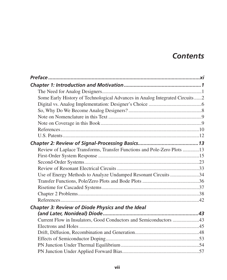
Contents
Preface
Intended Audience
Text Outline
Acknowledgments
1 Introduction and Motivation
The Need for Analog Designers
Some Early History of Technological Advances in Analog Integrated Circuits
Digital vs. Analog Implementation: Designer’s Choice
So, Why Do We Become Analog Designers?
Note on Nomenclature in this Text
Note on Coverage in this Book
References
U.S. Patents
2 Review of Signal-Processing Basics
Review of Laplace Transforms, Transfer Functions and Pole-Zero Plots
First-Order System Response
Second-Order Systems
Review of Resonant Electrical Circuits
Use of Energy Methods to Analyze Undamped Resonant Circuits
Transfer Functions, Pole/Zero Plots and Bode Plots
Risetime for Cascaded Systems
Chapter 2 Problems
References
3 Review of Diode Physics and the Ideal (and Later, Nonideal) Diode
Current Flow in Insulators, Good Conductors and Semiconductors
Electrons and Holes
Drift, Diffusion, Recombination and Generation
Effects of Semiconductor Doping
PN Junction Under Thermal Equilibrium
PN Junction Under Applied Forward Bias
Reverse Biased Diode
Ideal Diode Equation
Charge Storage in Diodes
Charge Storage in the Diode Under Forward Bias
Reverse Recovery in Bipolar Diodes
Reverse Breakdown
Taking a Look at a Diode Datasheet
Some Quick Comments on Schottky Diodes
Chapter 3 Problems
References
4 Bipolar Transistor Models
A Little Bit of History
Basic NPN Transistor
Transistor Models in Different Operating Regions
Low-Frequency Incremental Bipolar Transistor Model
High-Frequency Incremental Model
Reading a Transistor Datasheet
Limitations of Hybrid-Pi Model
Chapter 4 Problems
References
5 Basic Bipolar Transistor Amplifiers and Biasing
The Issue of Transistor Biasing
Example 5.1: Biasing example
Some Transistor Amplifiers
Example 5.2: Emitter follower design example
Example 5.3: Peaking amplifier
Chapter 5 Problems
References
6 Bandwidth Estimation Techniques and the Method of Open-Circuit Time Constants
Introduction to Open-Circuit Time Constants
Example 6.1: Elementary OCTC example
Transistor Amplifier Examples
Example 6.2: Common-emitter amplifier (revisited)
Example 6.3: Emitter-follower bandwidth estimate
Example 6.4: Differential amplifier
Example 6.5: Design case study using open-circuit time constants
Chapter 6 Problems
References
7 Advanced Transistor Amplifier Techniques
Worst-Case Open-Circuit Time Constant Calculations
Example 7.1: Estimating bandwidth of common-emitter amplifier with emitter degeneration
Example 7.2: Gain of differential amplifier with emitter degeneration
High-Frequency Output and Input Impedance of Emitter-Follower Buffers
Example 7.3: Emitter-follower output impedance
Example 7.4: Emitter-follower input impedance
Bootstrapping
Example 7.5: Bootstrapping an emitter-follower
Example 7.6: Another bootstrapping design example
Short-Circuit Time Constants
Example 7.7: Short-circuit time constants design example
Example 7.8: Peaking amplifier revisited
Example 7.9: Common-base amplifier
Example 7.10: Current amplifier
Pole Splitting
Example 7.11: Pole splitting
Chapter 7 Problems
References
8 High-Gain Bipolar Amplifiers and BJT Current Mirrors
The Need to Augment the Hybrid-Pi Model
Base-Width Modulation
Finding Parameters from a Transistor Datasheet
Common-Emitter Amplifier with Current Source Load
Building Blocks
Example 8.1: Incremental input resistance of emitter-follower
Example 8.2: Widlar current mirror
Example 8.3: Widlar mirror incremental output resistance
Example 8.4: Current mirror error due to mismatched VCEs
Example 8.5: Design example—high-gain amplifier
Example 8.6: Another high-gain amplifier example
Example 8.7: Another high-gain amplifier example (revisited)
Chapter 8 Problems
References
9 Introduction to MOSFET Devices and Basic MOS Amplifiers
Some Early History of Field-Effect Transistors
Qualitative Discussion of Basic MOS Devices
Figuring Out the V/I Curve of a MOS Device
Curve of a MOS Device
MOS Small-Signal Model (Low Frequency)
MOS Small-Signal Model (High Frequency)
Basic MOS Amplifiers
Example 9.1: MOS amplifier design example
Chapter 9 Problems
References
10 Bipolar Transistor Switching and the Charge Control Model
Introduction
Development of the Switching Models
Reverse-Active Region
Saturation
Junction Capacitances
Relationship Between Charge Control and Hybrid-Pi Parameters
Finding Junction Capacitances from the Datasheet
Manufacturers’ Testing
Charge Control Model Examples
Example 10.1: Transistor inverter with base current drive
Example 10.2: Transistor inverter with voltage drive
Example 10.3: Nonsaturating current switch
Emitter Switching
2N2222 Datasheet Excerpts
Chapter 10 Problems
References
11 Review of Feedback Systems
Introduction and Some Early History of Feedback Control
Invention of the Negative Feedback Amplifier
Control System Basics
Loop Transmission and Disturbance Rejection
Stability
Routh Stability Criterion
The Phase Margin and Gain Margin Tests
Relationship Between Damping Ratio and Phase Margin
Loop Compensation Techniques—Lead and Lag Networks
Parenthetical Comment on Some Interesting Feedback Loops
Example 11.1: Gain of +1 amplifier
Example 11.2: Gain of +10 amplifier
Example 11.3: Integral control of reactive load
Example 11.4: Photodiode amplifier
Example 11.5: MOSFET current source
Example 11.6: Maglev example
Appendix: MATLAB Scripts
Chapter 11 Problems
References
12 Basic Operational Amplifier Topologies and a Case Study
Basic Device Operation
Example 12.1: Case study: Design, analysis and simulation of a discrete operational amplifier
Brief Review of LM741 Op-Amp Schematic
Some Real-World Limitations of Operational Amplifiers
Example 12.2: Op-amp driving capacitive load
Chapter 12 Problems
References
13 Review of Current Feedback Operational Amplifiers
Conventional Voltage-Feedback Op-Amp and the Constant “Gain Bandwidth Product” Paradigm
Slew Rate Limitations in Conventional Op-Amps
Basic Current Feedback Op-Amp
Absence of Slew Rate Limit in Current Feedback Op-Amps
Example 13.1: An admittedly very crude current-feedback op-amp discrete design
Manufacturer’s Datasheet Information for a Current Feedback Amplifier
A More Detailed Model and Some Comments on Current-Feedback Op- Amp Limitations
Chapter 13 Problems
References
14 Analog Low-Pass Filters
Introduction
Review of Low-Pass Filter Basics
Butterworth Filter
Chebyshev Filter
Bessel Filter
Comparison of Responses of Different Filter Types
Filter Implementation
Example 14.1: Design example: Fifth-order Chebyshev filter with 0.5dB passband ripple
Example 14.2: Design Example: 40-Hz Sallen-Key with Adjustable Q
Example 14.3: Design case study: 1-MHz low-pass filter
Example 14.4: Alternate design using Butterworth filter
Chapter 14 Problems
References
15 Review of Passive Components and a Case Study in PC Board Layout
Resistors
Comments on Surface-Mount Resistors
Comments on Resistor Types
Capacitors
Inductors
Discussion of Printed-Circuit Board Layout Issues
Approximate Inductance of a PC Board Trace Above a Ground Plane
Example 15.1: Design case study—high-speed semiconductor laser diode driver
Chapter 15 Problems
References
16 Other Useful Design Techniques and Loose Ends
Thermal Circuits
Steady-State Model of Conductive Heat Transfer
Thermal Energy Storage
Using Thermal Circuit Analogies to Determine Static Semiconductor Junction Temperature
Mechanical Circuit Analogies
Mechanical system: Electrical system:
Example 16.1: Using mechanical circuit analogies
The Translinear Principle
Input Impedance of Infinitely Long Resistive Ladder
Transmission Lines 101
Example 16.2: Transmission line calculation
Node Equations and Cramer’s Rule
Example 16.3: Using Cramer’s rule to solve simultaneous linear equations
Finding Oscillation Modes
Example 16.4: Finding oscillation modes using MATLAB
Some Comments on Scaling Laws in Nature
Chapter 16 Problems
References
Index
What's on the CD-ROM?
CD-ROM License Agreement




 2023年江西萍乡中考道德与法治真题及答案.doc
 2012年重庆南川中考生物真题及答案.doc
 2013年江西师范大学地理学综合及文艺理论基础考研真题.doc
 2020年四川甘孜小升初语文真题及答案I卷.doc
 2020年注册岩土工程师专业基础考试真题及答案.doc
 2023-2024学年福建省厦门市九年级上学期数学月考试题及答案.doc
 2021-2022学年辽宁省沈阳市大东区九年级上学期语文期末试题及答案.doc
 2022-2023学年北京东城区初三第一学期物理期末试卷及答案.doc
 2018上半年江西教师资格初中地理学科知识与教学能力真题及答案.doc
 2012年河北国家公务员申论考试真题及答案-省级.doc
 2020-2021学年江苏省扬州市江都区邵樊片九年级上学期数学第一次质量检测试题及答案.doc
 2022下半年黑龙江教师资格证中学综合素质真题及答案.doc