RDA5802N/NS/NM
SINGLE-CHIP BROADCAST FM RADIO TUNER Rev.2.0–Mar.2011
1 General Description
is
The RDA5802N series
the newest generation
single-chip broadcast FM stereo radio tuner with fully
integrated synthesizer, IF selectivity, RDS/RBDS and
MPX decoder. The tuner uses the CMOS process,
support multi-interface and require the least external
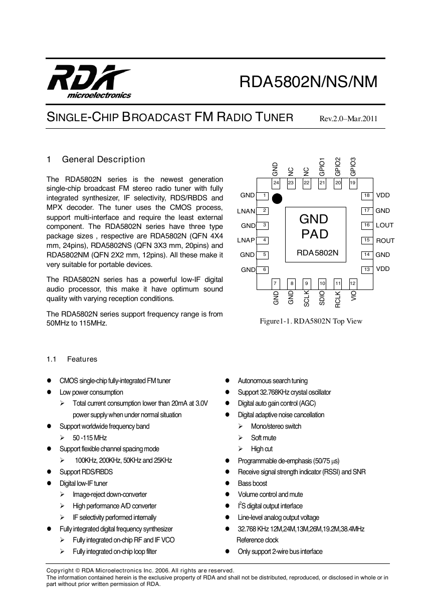
component. The RDA5802N series have three type
package sizes , respective are RDA5802N (QFN 4X4
mm, 24pins), RDA5802NS (QFN 3X3 mm, 20pins) and
RDA5802NM (QFN 2X2 mm, 12pins). All these make it
very suitable for portable devices.
The RDA5802N series has a powerful low-IF digital
audio processor, this make it have optimum sound
quality with varying reception conditions.
The RDA5802N series support frequency range is from
50MHz to 115MHz.
1.1 Features
Figure1-1. RDA5802N Top View
CMOS single-chip fully-integrated FM tuner
Autonomous search tuning
Low power consumption
Support 32.768KHz crystal oscillator
Total current consumption lower than 20mA at 3.0V
Digital auto gain control (AGC)
power supply when under normal situation
Digital adaptive noise cancellation
Support worldwide frequency band
Mono/stereo switch
50 -115 MHz
Support flexible channel spacing mode
Soft mute
High cut
100KHz, 200KHz, 50KHz and 25KHz
Programmable de-emphasis (50/75 s)
Support RDS/RBDS
Digital low-IF tuner
Image-reject down-converter
High performance A/D converter
IF selectivity performed internally
Receive signal strength indicator (RSSI) and SNR
Bass boost
Volume control and mute
I2S digital output interface
Line-level analog output voltage
Fully integrated digital frequency synthesizer
32.768 KHz 12M,24M,13M,26M,19.2M,38.4MHz
Fully integrated on-chip RF and IF VCO
Reference clock
Fully integrated on-chip loop filter
Only support 2-wire bus interface
Copyright © RDA Microelectronics Inc. 2006. All rights are reserved.
The information contained herein is the exclusive property of RDA and shall not be distributed, reproduced, or disclosed in whole or in
part without prior written permission of RDA.
234561717161514131889101112242322212019GNDPADGNDGNDLNAPGNDRDA 5802NVDDGNDLOUTGNDLNANROUTGND VDDGNDGNDSCLKSDIORCLKVIOGNDNCNCGPIO1GPIO2GPIO3�
RDA Microelectronics, Inc. RDA5802N/NS/NM FM Tuner V2.0
Directly support 32Ω resistance loading
Integrated LDO regulator
1.8 to 5.5 V operation voltage
Support QFN 4X4mm 24pins, QFN 3X3mm 20pins and
QFN 2x2mm 12pins three package types.
1.2
Applications
Cellular handsets
MP3, MP4 players
Portable radios
PDAs, Notebook
The information contained herein is the exclusive property of RDA and shall not be distributed, reproduced, or disclosed in whole or in
part without prior written permission of RDA.
Page 2 of 29
�
RDA Microelectronics, Inc. RDA5802N/NS/NM FM Tuner V2.0
Table of Contents
1 General Description .................................................................................................................................... 1
Features ......................................................................................................................................... 1
Applications .................................................................................................................................... 2
1.1
1.2
Table of Contents................................................................................................................................................. 3
2
Functional Description ............................................................................................................................... 4
FM Receiver .................................................................................................................................. 4
2.1
Synthesizer .................................................................................................................................... 4
2.2
Power Supply ................................................................................................................................ 5
2.3
2.4
RESET and Control Interface select ............................................................................................. 5
Control Interface ........................................................................................................................... 5
2.5
I2S Audio Data Interface ............................................................................................................... 5
2.6
2.7
GPIO Outputs ................................................................................................................................ 5
3 Electrical Characteristics ........................................................................................................................... 6
4 Receiver Characteristics ............................................................................................................................. 7
5
Serial Interface ............................................................................................................................................ 8
I2C Interface Timing ...................................................................................................................... 8
5.1
6 Register Definition ...................................................................................................................................... 9
9 Application Diagram................................................................................................................................. 19
RDA5802N Common Application : ............................................................................................ 19
Bill of Materials: ......................................................................................................................... 19
RDA5802NS Common Application: ........................................................................................... 20
Bill of Materials: ......................................................................................................................... 20
RDA5802NM Common Application: ......................................................................................... 21
Bill of Materials: ......................................................................................................................... 21
9.1
9.1.1
9.2
9.2.1
9.3
9.3.1
10 Physical Dimension ................................................................................................................................... 22
11 PCB Land Pattern ..................................................................................................................................... 25
12 Change List ................................................................................................................................................ 28
13 Notes: ....................................................................................................................................................... 28
14 Contact Information ................................................................................................................................. 29
The information contained herein is the exclusive property of RDA and shall not be distributed, reproduced, or disclosed in whole or in
part without prior written permission of RDA.
Page 3 of 29
�
RDA Microelectronics, Inc. RDA5802N/NS/NM FM Tuner V2.0
2 Functional Description
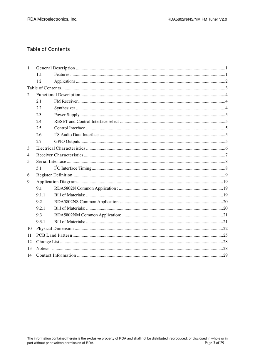
Figure 2-1. RDA5802N FM Tuner Block Diagram
2.1
FM Receiver
The receiver uses a digital low-IF architecture that
avoids
the difficulties associated with direct
conversion while delivering lower solution cost
and reduces complexity, and integrates a low
noise amplifier
the FM
broadcast band (50 to 115MHz), a multi-phase
image-reject mixer array, a programmable gain
control (PGA), a high resolution analog-to-digital
converters (ADCs), an audio DSP and a high-
fidelity digital-to-analog converters (DACs).
(LNA) supporting
The LNA has differential input ports (LNAP and
LNAN) and supports any input port by set
according registers bits (LNA_PORT_SEL[1:0]). It
default input common mode voltage is GND.
The limiter prevents overloading and limits the
amount of intermodulation products created by
strong adjacent channels.
The multi-phase mixer array down converts the
LNA output differential RF signal to low-IF, it also
has image-reject function and harmonic tones
rejection.
The PGA amplifies the mixer output IF signal and
then digitized with ADCs.
The DSP core finishes the channel selection, FM
demodulation, stereo MPX decoder and output
audio signal. The MPX decoder can autonomous
switch from stereo to mono to limit the output
noise.
The DACs convert digital audio signal to analog
and change the volume at same time. The DACs
has low-pass feature and -3dB frequency is about
30 KHz.
2.2 Synthesizer
The frequency synthesizer generates the local
oscillator signal which divide to multi-phase, then
be used to downconvert the RF input to a
constant low intermediate frequency (IF). The
synthesizer reference clock is 32.768 KHz.
The synthesizer frequency is defined by bits
CHAN[9:0] with
to
115MHz.
from 50MHz
the range
The information contained herein is the exclusive property of RDA and shall not be distributed, reproduced, or disclosed in whole or in
part without prior written permission of RDA.
Page 4 of 29
IADCLDACRDACQADC+-Audio DSP Coredigital filter MPX decoder stereo/monoaudioVCOSynthesizerGPIOInterfaceBusRSSIVIOSDIOSCLKMCUGPIORDA5802NLOUTROUTLNANLNAPRCLK2.7-5.5 V32.768 KHzVDDLDOLimiterLNAIPGAQPGARDS /RBDS�
RDA Microelectronics, Inc. RDA5802N/NS/NM FM Tuner V2.0
2.3 Power Supply
The RDA5802N
integrated one LDO which
supplies power to the chip. The external supply
voltage range is 1.8-5.5 V.
2.4 RESET and Control Interface select
The RDA5802N is RESET itself When VIO is
Power up. And also support soft reset by trigger
02H BIT1 from 0 to 1. T he
only
support I2C control interface bus mode.
RDA5802N
2.5 Control Interface
The RDA5802N only supports
interface.
I2C control
I2C
to
interface
is compliant
I2C Bus
The
Specification 2.1. It includes two pins: SCLK and
SDIO. A I2C interface transfer begins with START
condition, a command byte and data bytes, each
byte has a followed ACK (or NACK) bit, and ends
with STOP condition. The command byte includes
a 7-bit chip address (0010000b) and a R/W bit.
The ACK (or NACK) is always sent out by receiver.
When in write transfer, data bytes is written out
from MCU, and when in read transfer, data bytes
is read out from RDA5802N. There is no visible
register address in I2C interface transfers. The I2C
interface has a fixed start register address (0x02h
for write transfer and 0x0Ah for read transfer), and
an internal incremental address counter. If register
address meets the end of register file, 0x3Ah,
register address will wrap back to 0x00h. For write
transfer, MCU programs registers from register
0x02h high byte, then register 0x02h low byte,
then register 0x03h high byte, till the last register.
RDA5802N always gives out ACK after every byte,
and MCU gives out STOP condition when register
programming is finished. For read transfer, after
command byte from MCU, RDA5802N sends out
register 0x0Ah high byte, then register 0x0Ah low
byte, then register 0x0Bh high byte, till receives
NACK from MCU. MCU gives out ACK for data
bytes besides last data byte. MCU gives out
NACK for last data byte, and then RDA5802N will
return the bus to MCU, and MCU will give out
STOP condition.
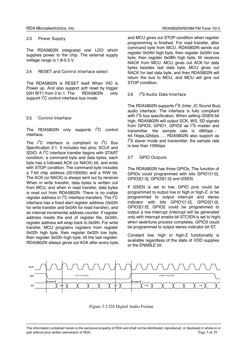
2.6
I2S Audio Data Interface
The RDA5802N supports I2S (Inter_IC Sound Bus)
audio interface. The interface is fully compliant
with I2S bus specification. When setting I2SEN bit
high, RDA5802N will output SCK, WS, SD signals
from GPIO3, GPIO1, GPIO2 as I2S master and
is 48Kbps ,
transmitter,
44.1kbps,32kbps….. RDA5802N also support as
I2S slaver mode and transmitter, the sample rate
is less than 100kbps.
the sample
rate
2.7 GPIO Outputs
The RDA5802N has three GPIOs. The function of
GPIOs could programmed with bits GPIO1[1:0],
GPIO2[1:0], GPIO3[1:0] and I2SEN.
to output
If I2SEN is set to low, GPIO pins could be
programmed to output low or high or high-Z, or be
programmed
interrupt and stereo
indicator with bits GPIO1[1:0], GPIO2[1:0],
GPIO3[1:0]. GPIO2 could be programmed to
output a low interrupt (interrupt will be generated
only with interrupt enable bit STCIEN is set to high)
when seek/tune process completes. GPIO3 could
be programmed to output stereo indicator bit ST.
Constant low, high or high-Z functionality is
available regardless of the state of VDD supplies
or the ENABLE bit.
Figure 3-2 I2S Digital Audio Format
The information contained herein is the exclusive property of RDA and shall not be distributed, reproduced, or disclosed in whole or in
part without prior written permission of RDA.
Page 5 of 29
SCKMSBSDWS1 SCKLEFT CHANNELLSBMSB1 SCKRIGHT CHANNELLSB�
RDA Microelectronics, Inc. RDA5802N/NS/NM FM Tuner V2.0
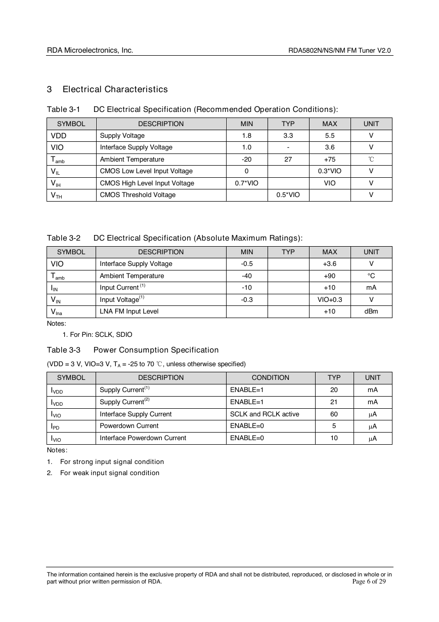
3 Electrical Characteristics
Table 3-1 DC Electrical Specification (Recommended Operation Conditions):
SYMBOL
DESCRIPTION
MIN
TYP
MAX
UNIT
Supply Voltage
Interface Supply Voltage
Ambient Temperature
CMOS Low Level Input Voltage
1.8
1.0
-20
0
CMOS High Level Input Voltage
0.7*VIO
3.3
-
27
CMOS Threshold Voltage
0.5*VIO
5.5
3.6
+75
0.3*VIO
VIO
V
V
℃
V
V
V
VDD
VIO
Tamb
VIL
VIH
VTH
Table 3-2 DC Electrical Specification (Absolute Maximum Ratings):
SYMBOL
DESCRIPTION
VIO
Tamb
IIN
VIN
Vlna
Notes:
Interface Supply Voltage
Ambient Temperature
Input Current (1)
Input Voltage(1)
LNA FM Input Level
MIN
-0.5
-40
-10
-0.3
TYP
MAX
+3.6
+90
+10
VIO+0.3
UNIT
V
°C
mA
V
+10
dBm
1. For Pin: SCLK, SDIO
Table 3-3
Power Consumption Specification
(VDD = 3 V, VIO=3 V, TA = -25 to 70 ℃, unless otherwise specified)
SYMBOL
DESCRIPTION
CONDITION
TYP
UNIT
IVDD
IVDD
IVIO
IPD
IVIO
Notes:
Supply Current(1)
Supply Current(2)
ENABLE=1
ENABLE=1
Interface Supply Current
SCLK and RCLK active
Powerdown Current
Interface Powerdown Current
ENABLE=0
ENABLE=0
20
21
60
5
10
mA
mA
A
A
A
1. For strong input signal condition
2. For weak input signal condition
The information contained herein is the exclusive property of RDA and shall not be distributed, reproduced, or disclosed in whole or in
part without prior written permission of RDA.
Page 6 of 29
�
RDA Microelectronics, Inc. RDA5802N/NS/NM FM Tuner V2.0
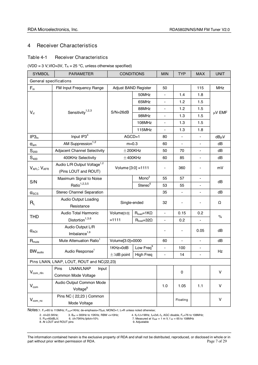
4 Receiver Characteristics
Table 4-1 Receiver Characteristics
(VDD = 3 V,VIO=3V, TA = 25 °C, unless otherwise specified)
SYMBOL
PARAMETER
CONDITIONS
MIN
TYP
MAX
UNIT
General specifications
FM Input Frequency Range
Adjust BAND Register
50
115
MHz
Fin
Vrf
IP3in
αam
S200
S400
VAFL; VAFR
S/N
αSCS
RL
THD
αAOI
Rmute
Sensitivity
1,2,3
S/N=26dB
50MHz
65MHz
88MHz
98MHz
108MHz
115MHz
Input IP34
AM Suppression
1,2
Adjacent Channel Selectivity
400KHz Selectivity
Audio L/R Output Voltage1,2
(Pins LOUT and ROUT)
Maximum Signal to Noise
Ratio
1,2,3,5
AGCD=1
m=0.3
±200KHz
±400KHz
Mono2
Stereo6
Stereo Channel Separation
Audio Output Loading
Resistance
Single-ended
Audio Total Harmonic
Volume[3:0]
Rload=1KΩ
Distortion
1,3,6
Audio Output L/R
Imbalance1,6
=1111
Rload=32Ω
Mute Attenuation Ratio1
Volume[3:0]=0000
60
BWaudio
Audio Response1
1KHz=0dB
Low Freq9
±3dB point
High Freq
Pins LNAN, LNAP, LOUT, ROUT and NC(22,23)
Vcom_rfin
Vcom
Vcom_nc
Pins
LNAN/LNAP
Input
Common Mode Voltage
Audio Output Common Mode
Voltage8
Pins NC ( 22,23 ) Common
Mode Voltage
Volume [3:0] =1111
-
360
1.4
1.2
1.2
1.3
1.3
1.3
-
-
70
85
57
55
-
-
0.15
0.2
-
-
100
14
0
1.8
1.5
1.5
1.5
1.5
1.8
-
-
-
-
-
-
-
-
-
0.2
-
0.05
-
-
-
-
-
-
-
-
-
80
60
50
60
55
53
35
32
-
-
-
-
-
1.0
1.05
1.1
Floating
V EMF
dBV
dB
dB
dB
mV
dB
dB
Ω
%
dB
dB
Hz
V
V
V
Notes:1. Fin=65 to 115MHz; Fmod=1KHz; de-emphasis=75s; MONO=1; L=R unless noted otherwise;
2. f=22.5KHz; 3. BAF = 300Hz to 15KHz, RBW <=10Hz; 4. |f2-f1|>1MHz, f0=2xf1-f2, AGC disable, Fin=76 to 108MHz;
5. PRF=60dBUV; 6. f=75KHz,fpilot=10% 7. Measured at VEMF = 1 m V, f RF = 65 to 108MHz
8. At LOUT and ROUT pins 9. Adjustable
The information contained herein is the exclusive property of RDA and shall not be distributed, reproduced, or disclosed in whole or in
part without prior written permission of RDA.
Page 7 of 29
�
RDA Microelectronics, Inc. RDA5802N/NS/NM FM Tuner V2.0
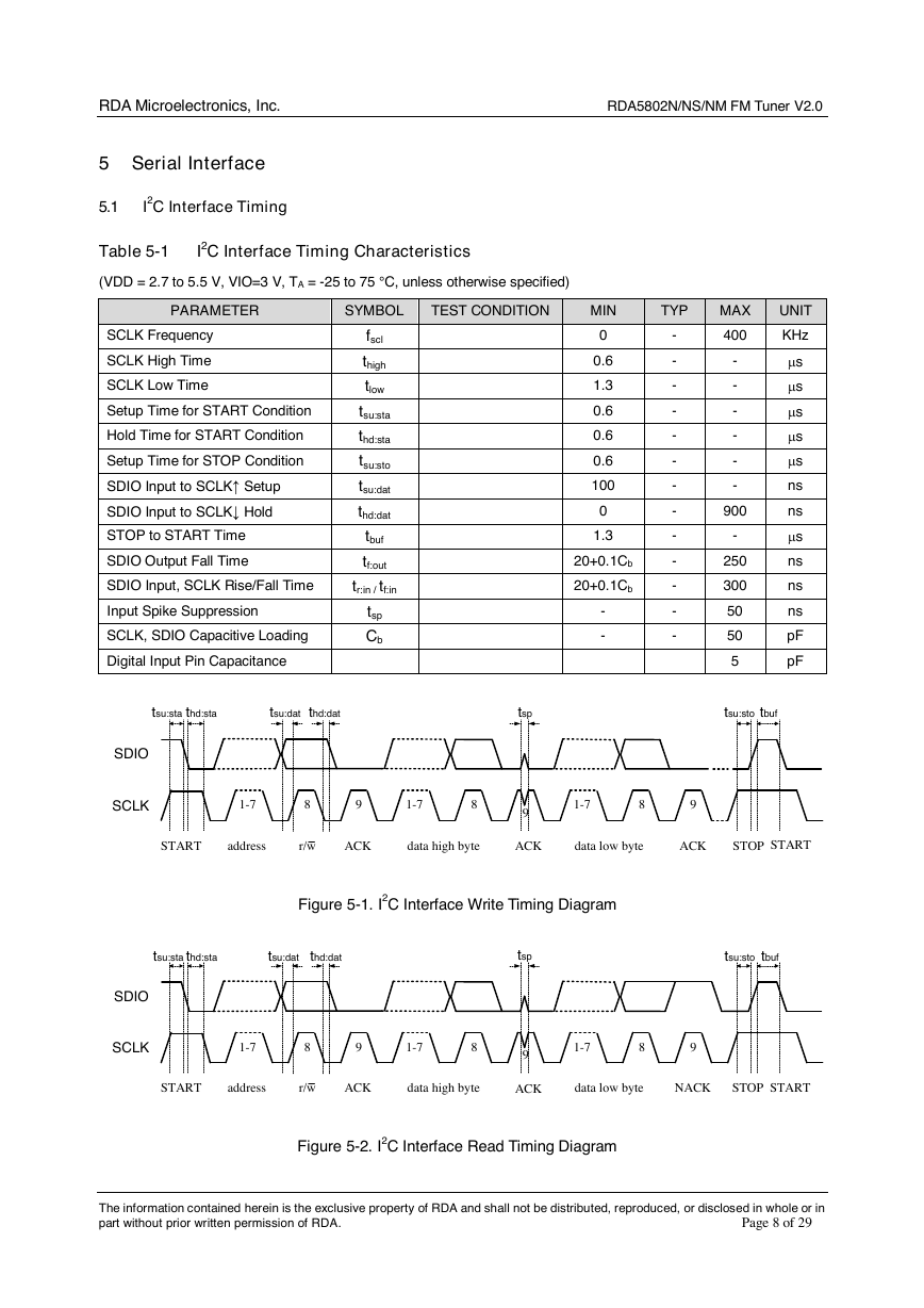
5 Serial Interface
5.1
I2C Interface Timing
Table 5-1
I2C Interface Timing Characteristics
(VDD = 2.7 to 5.5 V, VIO=3 V, TA = -25 to 75 °C, unless otherwise specified)
PARAMETER
SYMBOL
TEST CONDITION
MIN
TYP
MAX
UNIT
SCLK Frequency
SCLK High Time
SCLK Low Time
Setup Time for START Condition
Hold Time for START Condition
Setup Time for STOP Condition
SDIO Input to SCLK↑ Setup
SDIO Input to SCLK↓ Hold
STOP to START Time
SDIO Output Fall Time
fscl
thigh
tlow
tsu:sta
thd:sta
tsu:sto
tsu:dat
thd:dat
tbuf
tf:out
SDIO Input, SCLK Rise/Fall Time
tr:in / tf:in
Input Spike Suppression
SCLK, SDIO Capacitive Loading
Digital Input Pin Capacitance
tsp
Cb
0
0.6
1.3
0.6
0.6
0.6
100
0
1.3
20+0.1Cb
20+0.1Cb
-
-
-
-
-
-
-
-
-
-
-
-
-
-
-
400
KHz
-
-
-
-
-
-
900
-
250
300
50
50
5
s
s
s
s
s
ns
ns
s
ns
ns
ns
pF
pF
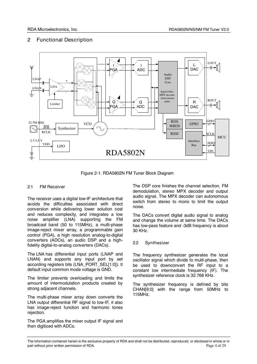
Figure 5-1. I2C Interface Write Timing Diagram
Figure 5-2. I2C Interface Read Timing Diagram
The information contained herein is the exclusive property of RDA and shall not be distributed, reproduced, or disclosed in whole or in
part without prior written permission of RDA.
Page 8 of 29
SCLKSDIO1-7891-7891-789STARTACKdata high byteACKr/waddressdata low byteACKSTOPtsu:stathd:statspSTARTtsu:stotbuftsu:datthd:datSCLKSDIO1-7891-7891-789STARTACKdata high byteACKr/waddressdata low byteNACKSTOPtspSTARTtbuftsu:stathd:statsu:datthd:dattsu:sto�


 2023年江西萍乡中考道德与法治真题及答案.doc
 2012年重庆南川中考生物真题及答案.doc
 2013年江西师范大学地理学综合及文艺理论基础考研真题.doc
 2020年四川甘孜小升初语文真题及答案I卷.doc
 2020年注册岩土工程师专业基础考试真题及答案.doc
 2023-2024学年福建省厦门市九年级上学期数学月考试题及答案.doc
 2021-2022学年辽宁省沈阳市大东区九年级上学期语文期末试题及答案.doc
 2022-2023学年北京东城区初三第一学期物理期末试卷及答案.doc
 2018上半年江西教师资格初中地理学科知识与教学能力真题及答案.doc
 2012年河北国家公务员申论考试真题及答案-省级.doc
 2020-2021学年江苏省扬州市江都区邵樊片九年级上学期数学第一次质量检测试题及答案.doc
 2022下半年黑龙江教师资格证中学综合素质真题及答案.doc