www.ti.com.cn
ZHCSA48A –JULY 2012 –REVISED OCTOBER 2012
1/2 H
: DRV8844
(IC)
DRV8844
1
2•
•
•
•
•
1/2 H
(DC)
–
DC
–
–
24V 25°C
MOSFET
2.5A
±30V
3.3V 10mA
(LDO)
IN/IN
8V
60V
•
•
•
•
•
•
•
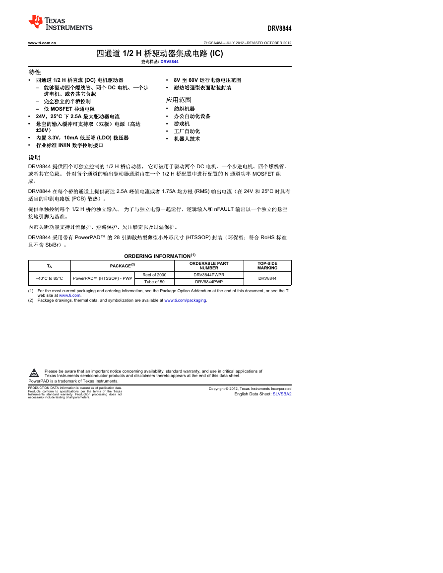
DRV8844
1/2 H
DC
1/2 H
N
MOSFET
DRV8844
2.5A
1.75A
(RMS)
24V
25°C
(PCB)
1/2 H
nFAULT
DRV8844
PowerPAD™ 28
(HTSSOP)
RoHS
Sb/Br
TA
ORDERING INFORMATION(1)
PACKAGE(2)
–40°C to 85°C
PowerPAD™ (HTSSOP) - PWP
Reel of 2000
Tube of 50
ORDERABLE PART
NUMBER
DRV8844PWPR
DRV8844PWP
TOP-SIDE
MARKING
DRV8844
(1) For the most current packaging and ordering information, see the Package Option Addendum at the end of this document, or see the TI
web site at www.ti.com.
(2) Package drawings, thermal data, and symbolization are available at www.ti.com/packaging.
1
Please be aware that an important notice concerning availability, standard warranty, and use in critical applications of
Texas Instruments semiconductor products and disclaimers thereto appears at the end of this data sheet.
2PowerPAD is a trademark of Texas Instruments.
PRODUCTION DATA information is current as of publication date.
Products conform to specifications per the terms of
the Texas
Instruments standard warranty. Production processing does not
necessarily include testing of all parameters.
Copyright © 2012, Texas Instruments Incorporated
English Data Sheet: SLVSBA2
�
DRV8844
ZHCSA48A –JULY 2012 –REVISED OCTOBER 2012
www.ti.com.cn
DEVICE INFORMATION
Functional Block Diagram
2
Copyright © 2012, Texas Instruments Incorporated
�
www.ti.com.cn
ZHCSA48A –JULY 2012 –REVISED OCTOBER 2012
NAME
PIN
I/O(1)
DESCRIPTION
EXTERNAL COMPONENTS
OR CONNECTIONS
POWER AND GROUND
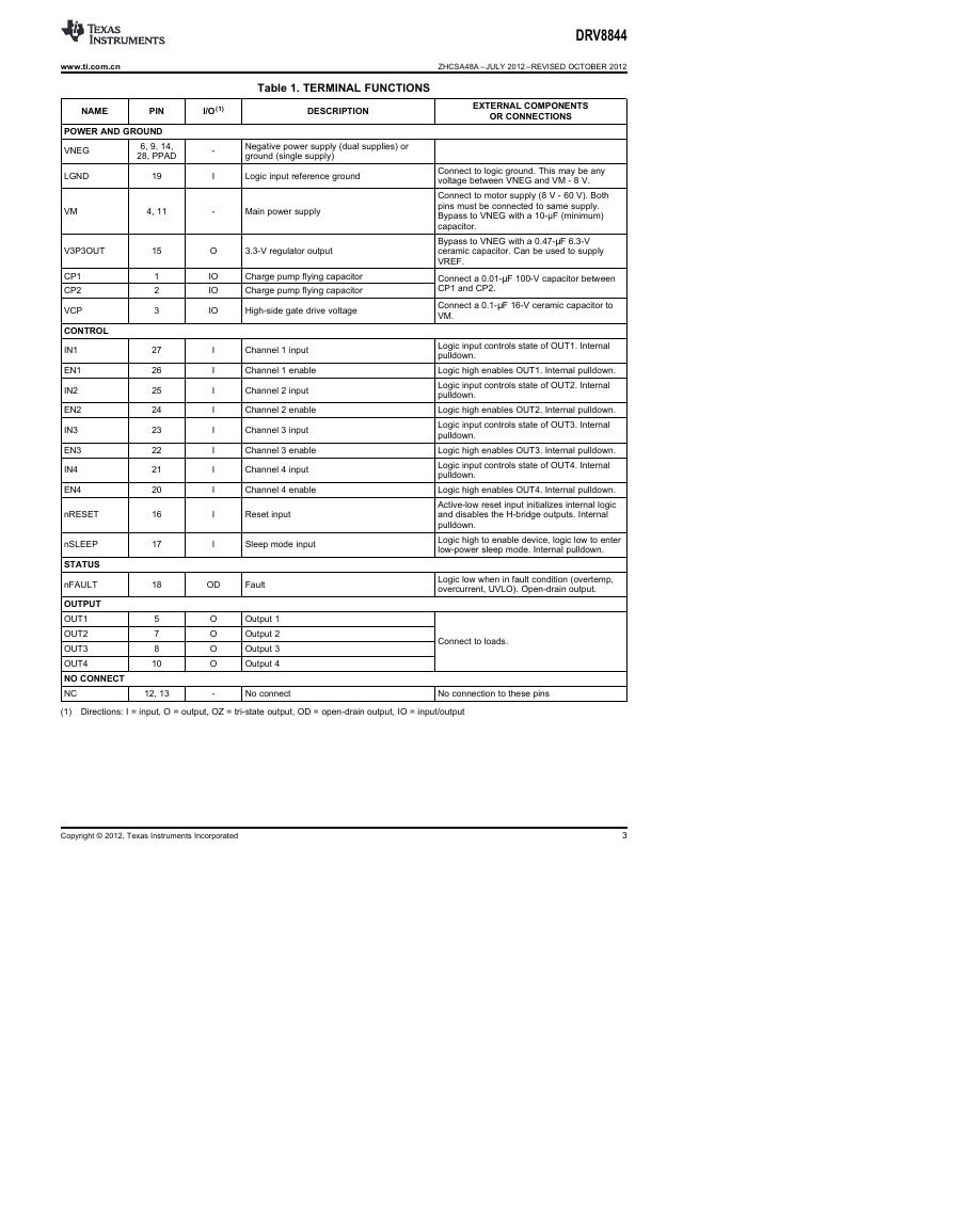
Table 1. TERMINAL FUNCTIONS
DRV8844
VNEG
LGND
VM
V3P3OUT
CP1
CP2
VCP
CONTROL
IN1
EN1
IN2
EN2
IN3
EN3
IN4
EN4
nRESET
nSLEEP
STATUS
nFAULT
OUTPUT
OUT1
OUT2
OUT3
OUT4
NO CONNECT
NC
6, 9, 14,
28, PPAD
19
4, 11
15
1
2
3
27
26
25
24
23
22
21
20
16
17
18
5
7
8
10
12, 13
-
I
-
O
IO
IO
IO
I
I
I
I
I
I
I
I
I
I
Negative power supply (dual supplies) or
ground (single supply)
Logic input reference ground
Main power supply
3.3-V regulator output
Charge pump flying capacitor
Charge pump flying capacitor
High-side gate drive voltage
Channel 1 input
Channel 1 enable
Channel 2 input
Channel 2 enable
Channel 3 input
Channel 3 enable
Channel 4 input
Channel 4 enable
Reset input
Sleep mode input
OD
Fault
O
O
O
O
-
Output 1
Output 2
Output 3
Output 4
No connect
Connect to logic ground. This may be any
voltage between VNEG and VM - 8 V.
Connect to motor supply (8 V - 60 V). Both
pins must be connected to same supply.
Bypass to VNEG with a 10-µF (minimum)
capacitor.
Bypass to VNEG with a 0.47-μF 6.3-V
ceramic capacitor. Can be used to supply
VREF.
Connect a 0.01-μF 100-V capacitor between
CP1 and CP2.
Connect a 0.1-μF 16-V ceramic capacitor to
VM.
Logic input controls state of OUT1. Internal
pulldown.
Logic high enables OUT1. Internal pulldown.
Logic input controls state of OUT2. Internal
pulldown.
Logic high enables OUT2. Internal pulldown.
Logic input controls state of OUT3. Internal
pulldown.
Logic high enables OUT3. Internal pulldown.
Logic input controls state of OUT4. Internal
pulldown.
Logic high enables OUT4. Internal pulldown.
Active-low reset input initializes internal logic
and disables the H-bridge outputs. Internal
pulldown.
Logic high to enable device, logic low to enter
low-power sleep mode. Internal pulldown.
Logic low when in fault condition (overtemp,
overcurrent, UVLO). Open-drain output.
Connect to loads.
No connection to these pins
(1) Directions: I = input, O = output, OZ = tri-state output, OD = open-drain output, IO = input/output
Copyright © 2012, Texas Instruments Incorporated
3
�
DRV8844
ZHCSA48A –JULY 2012 –REVISED OCTOBER 2012
www.ti.com.cn
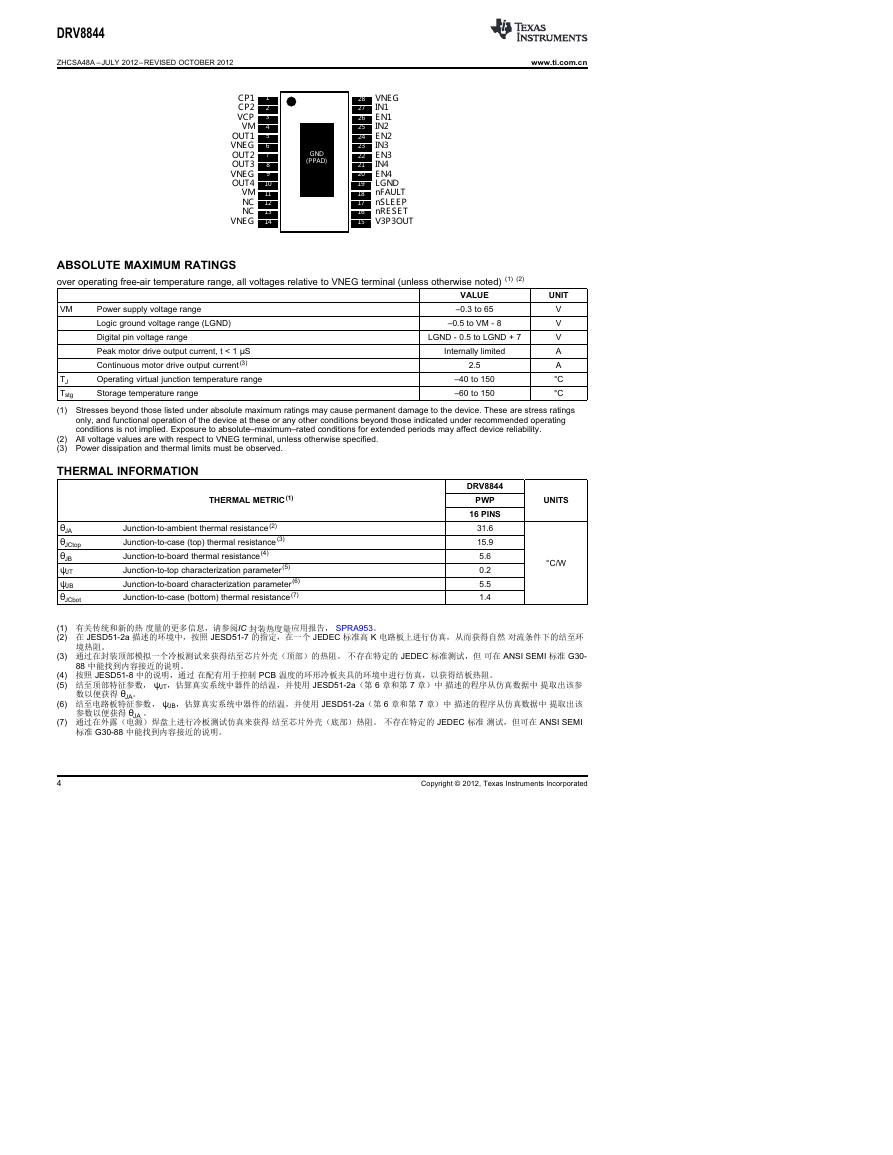
CP1
CP2
VCP
VM
OUT1
VNEG
OUT2
OUT3
VNEG
OUT4
VM
NC
NC
VNEG
1
2
3
4
5
6
7
8
9
10
11
12
13
14
GND
(PPAD)
28
27
26
25
24
23
22
21
20
19
18
17
16
15
VNEG
IN1
EN1
IN2
EN2
IN3
EN3
IN4
EN4
LGND
nFAULT
nSLEEP
nRESET
V3P3OUT
ABSOLUTE MAXIMUM RATINGS
over operating free-air temperature range, all voltages relative to VNEG terminal (unless otherwise noted) (1) (2)
VM
Power supply voltage range
Logic ground voltage range (LGND)
Digital pin voltage range
Peak motor drive output current, t < 1 μS
Continuous motor drive output current (3)
Operating virtual junction temperature range
Storage temperature range
TJ
Tstg
(1) Stresses beyond those listed under absolute maximum ratings may cause permanent damage to the device. These are stress ratings
–40 to 150
–60 to 150
only, and functional operation of the device at these or any other conditions beyond those indicated under recommended operating
conditions is not implied. Exposure to absolute–maximum–rated conditions for extended periods may affect device reliability.
(2) All voltage values are with respect to VNEG terminal, unless otherwise specified.
(3) Power dissipation and thermal limits must be observed.
VALUE
–0.3 to 65
–0.5 to VM - 8
LGND - 0.5 to LGND + 7
Internally limited
2.5
UNIT
V
V
V
A
A
°C
°C
THERMAL INFORMATION
THERMAL METRIC(1)
θJA
θJCtop
θJB
ψJT
ψJB
θJCbot
Junction-to-ambient thermal resistance(2)
Junction-to-case (top) thermal resistance (3)
Junction-to-board thermal resistance (4)
Junction-to-top characterization parameter(5)
Junction-to-board characterization parameter(6)
Junction-to-case (bottom) thermal resistance(7)
DRV8844
PWP
16 PINS
31.6
15.9
5.6
0.2
5.5
1.4
UNITS
°C/W
(1) 有关传统和新的热 度量的更多信息,请参阅IC 封装热度量应用报告, SPRA953。
(2) 在 JESD51-2a 描述的环境中,按照 JESD51-7 的指定,在一个 JEDEC 标准高 K 电路板上进行仿真,从而获得自然 对流条件下的结至环
(3) 通过在封装顶部模拟一个冷板测试来获得结至芯片外壳(顶部)的热阻。 不存在特定的 JEDEC 标准测试,但 可在 ANSI SEMI 标准 G30-
(4) 按照 JESD51-8 中的说明,通过 在配有用于控制 PCB 温度的环形冷板夹具的环境中进行仿真,以获得结板热阻。
(5) 结至顶部特征参数, ψJT,估算真实系统中器件的结温,并使用 JESD51-2a(第 6 章和第 7 章)中 描述的程序从仿真数据中 提取出该参
(6) 结至电路板特征参数, ψJB,估算真实系统中器件的结温,并使用 JESD51-2a(第 6 章和第 7 章)中 描述的程序从仿真数据中 提取出该
(7) 通过在外露(电源)焊盘上进行冷板测试仿真来获得 结至芯片外壳(底部)热阻。 不存在特定的 JEDEC 标准 测试,但可在 ANSI SEMI
境热阻。
88 中能找到内容接近的说明。
数以便获得 θJA。
参数以便获得 θJA 。
标准 G30-88 中能找到内容接近的说明。
空白
4
Copyright © 2012, Texas Instruments Incorporated
�
www.ti.com.cn
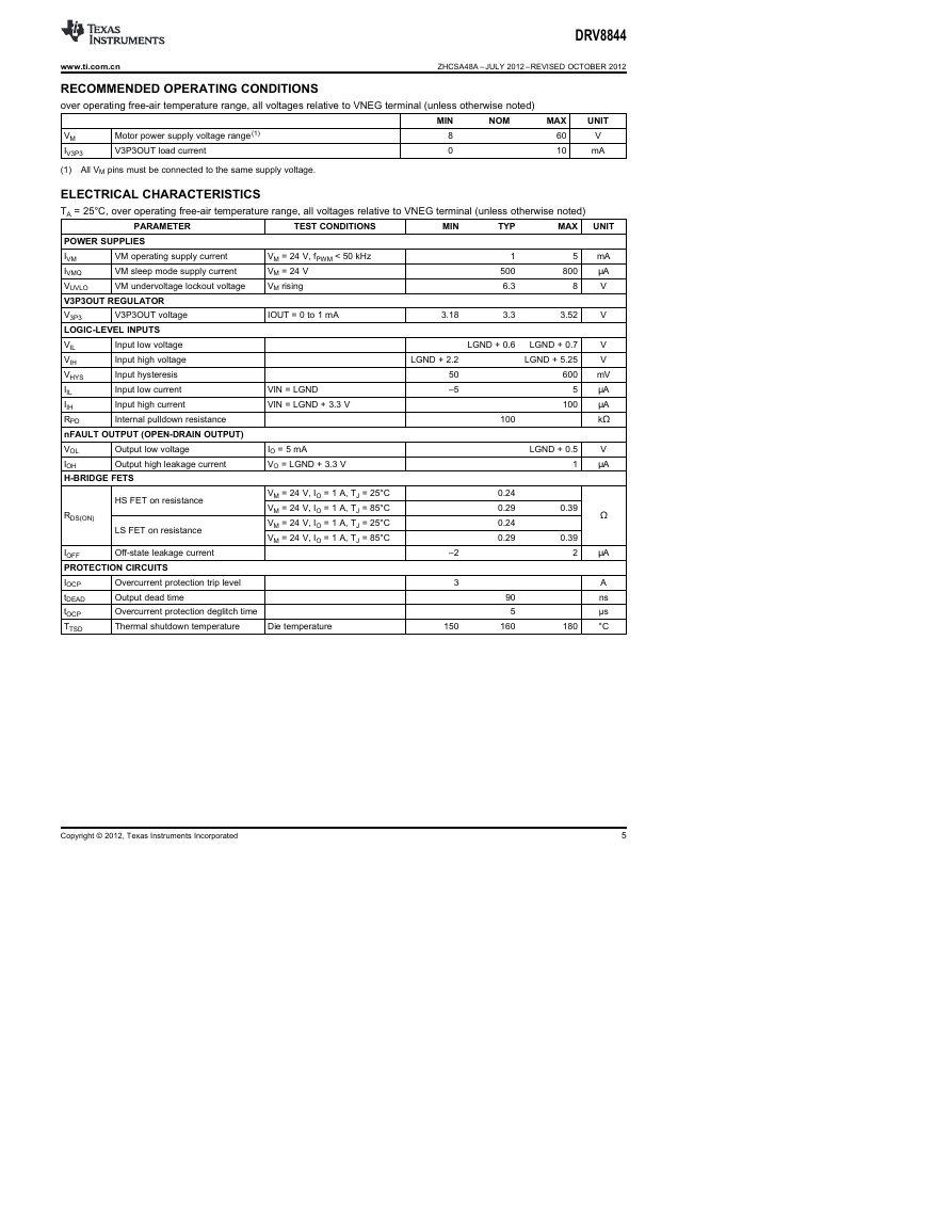
RECOMMENDED OPERATING CONDITIONS
over operating free-air temperature range, all voltages relative to VNEG terminal (unless otherwise noted)
ZHCSA48A –JULY 2012 –REVISED OCTOBER 2012
DRV8844
Motor power supply voltage range(1)
V3P3OUT load current
VM
IV3P3
(1) All VM pins must be connected to the same supply voltage.
ELECTRICAL CHARACTERISTICS
TA = 25°C, over operating free-air temperature range, all voltages relative to VNEG terminal (unless otherwise noted)
PARAMETER
TEST CONDITIONS
MIN
NOM
MIN
8
0
MAX
60
10
UNIT
V
mA
V3P3OUT voltage
VM operating supply current
VM sleep mode supply current
VM undervoltage lockout voltage
POWER SUPPLIES
IVM
IVMQ
VUVLO
V3P3OUT REGULATOR
V3P3
LOGIC-LEVEL INPUTS
VIL
VIH
VHYS
IIL
IIH
RPD
nFAULT OUTPUT (OPEN-DRAIN OUTPUT)
VOL
IOH
H-BRIDGE FETS
Input low voltage
Input high voltage
Input hysteresis
Input low current
Input high current
Internal pulldown resistance
Output low voltage
Output high leakage current
RDS(ON)
HS FET on resistance
LS FET on resistance
Off-state leakage current
IOFF
PROTECTION CIRCUITS
IOCP
tDEAD
tOCP
TTSD
Overcurrent protection trip level
Output dead time
Overcurrent protection deglitch time
Thermal shutdown temperature
VM = 24 V, fPWM < 50 kHz
VM = 24 V
VM rising
IOUT = 0 to 1 mA
3.18
TYP
1
500
6.3
3.3
MAX
UNIT
5
800
8
mA
μA
V
3.52
V
VIN = LGND
VIN = LGND + 3.3 V
IO = 5 mA
VO = LGND + 3.3 V
VM = 24 V, IO = 1 A, TJ = 25°C
VM = 24 V, IO = 1 A, TJ = 85°C
VM = 24 V, IO = 1 A, TJ = 25°C
VM = 24 V, IO = 1 A, TJ = 85°C
Die temperature
LGND + 0.6
LGND + 2.2
50
–5
100
0.24
0.29
0.24
0.29
90
5
160
–2
3
150
LGND + 0.7
LGND + 5.25
600
5
100
LGND + 0.5
1
0.39
0.39
2
180
V
V
mV
μA
μA
kΩ
V
μA
Ω
μA
A
ns
µs
°C
Copyright © 2012, Texas Instruments Incorporated
5
�
DRV8844
ZHCSA48A –JULY 2012 –REVISED OCTOBER 2012
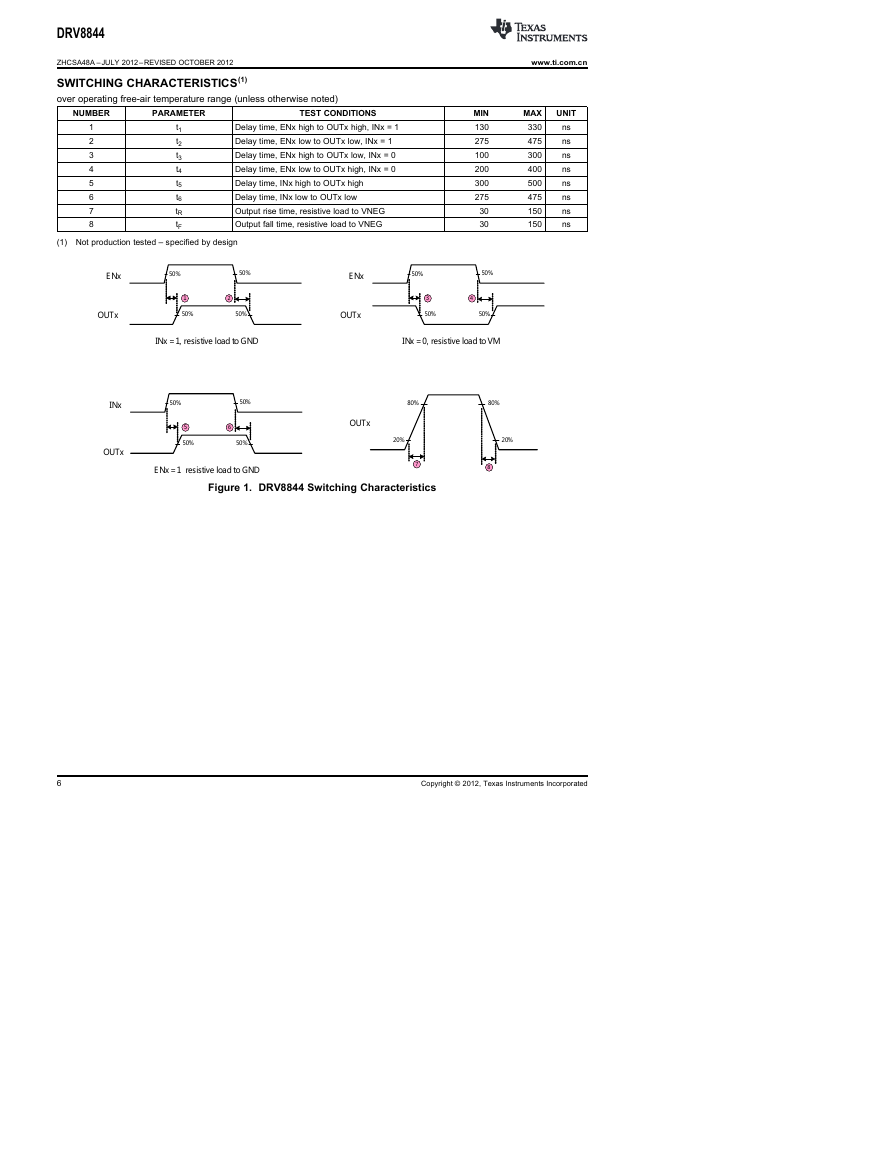
SWITCHING CHARACTERISTICS(1)
over operating free-air temperature range (unless otherwise noted)
NUMBER
PARAMETER
TEST CONDITIONS
1
2
3
4
5
6
7
8
t1
t2
t3
t4
t5
t6
tR
tF
Delay time, ENx high to OUTx high, INx = 1
Delay time, ENx low to OUTx low, INx = 1
Delay time, ENx high to OUTx low, INx = 0
Delay time, ENx low to OUTx high, INx = 0
Delay time, INx high to OUTx high
Delay time, INx low to OUTx low
Output rise time, resistive load to VNEG
Output fall time, resistive load to VNEG
(1) Not production tested – specified by design
www.ti.com.cn
MAX
330
475
300
400
500
475
150
150
UNIT
ns
ns
ns
ns
ns
ns
ns
ns
MIN
130
275
100
200
300
275
30
30
ENx
OUTx
INx
OUTx
50%
50%
1
50%
2
50%
ENx
OUTx
50%
50%
3
50%
4
50%
INx =1, resistiveloadtoGND
INx =0, resistiveloadtoVM
50%
50%
80%
80%
5
50%
6
50%
ENx =1 resistiveloadtoGND
OUTx
20%
7
20%
8
Figure 1. DRV8844 Switching Characteristics
6
Copyright © 2012, Texas Instruments Incorporated
�
www.ti.com.cn
ZHCSA48A –JULY 2012 –REVISED OCTOBER 2012
FUNCTIONAL DESCRIPTION
Output Stage
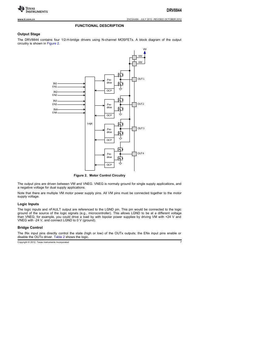
The DRV8844 contains four 1/2-H-bridge drivers using N-channel MOSFETs. A block diagram of the output
circuitry is shown in Figure 2.
DRV8844
VM
VM
VM
OUT 1
OUT2
OUT 3
OUT4
IN1
EN1
IN2
EN2
IN3
EN3
IN4
EN4
Logic
Pre-
drive
OCP
Pre-
drive
OCP
Pre-
drive
OCP
Pre-
drive
OCP
Figure 2. Motor Control Circuitry
The output pins are driven between VM and VNEG. VNEG is normaly ground for single supply applications, and
a negative voltage for dual supply applications.
Note that there are multiple VM motor power supply pins. All VM pins must be connected together to the motor
supply voltage.
Logic Inputs
The logic inputs and nFAULT output are referenced to the LGND pin. This pin would be connected to the logic
ground of the source of the logic signals (e.g., microcontroller). This allows LGND to be at a different voltage
than VNEG; for example, you could drive a load by with bipolar power supplies by driving VM with +24 V and
VNEG with -24 V, and connect LGND to 0 V (ground).
Bridge Control
The INx input pins directly control the state (high or low) of the OUTx outputs; the ENx input pins enable or
disable the OUTx driver. Table 2 shows the logic.
Copyright © 2012, Texas Instruments Incorporated
7
�
DRV8844
ZHCSA48A –JULY 2012 –REVISED OCTOBER 2012
www.ti.com.cn
Table 2. H-Bridge Logic
ENx
0
1
1
OUTx
Z
L
H
INx
X
0
1
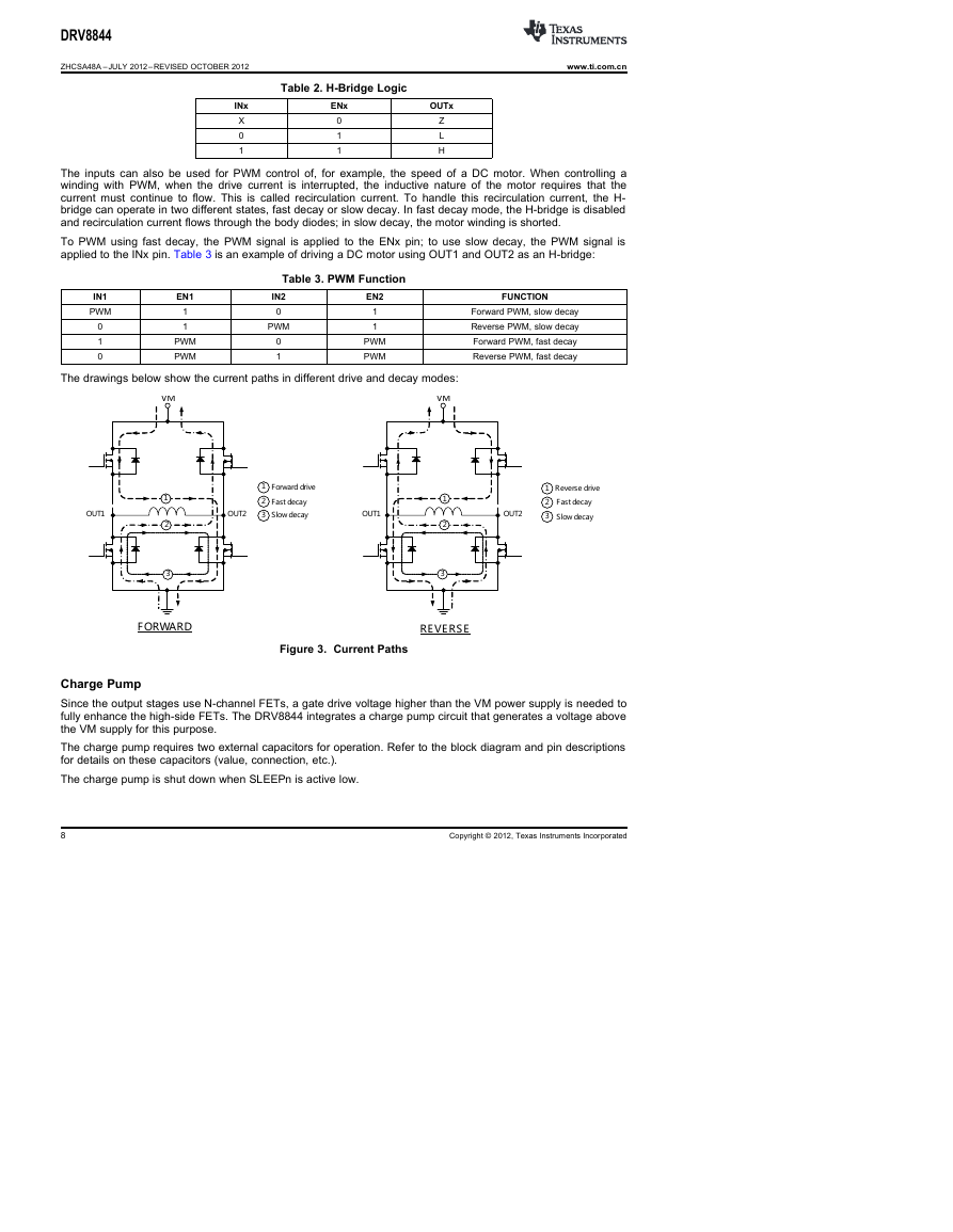
The inputs can also be used for PWM control of, for example, the speed of a DC motor. When controlling a
winding with PWM, when the drive current is interrupted, the inductive nature of the motor requires that the
current must continue to flow. This is called recirculation current. To handle this recirculation current, the H-
bridge can operate in two different states, fast decay or slow decay. In fast decay mode, the H-bridge is disabled
and recirculation current flows through the body diodes; in slow decay, the motor winding is shorted.
To PWM using fast decay, the PWM signal
applied to the INx pin. Table 3 is an example of driving a DC motor using OUT1 and OUT2 as an H-bridge:
is applied to the ENx pin; to use slow decay, the PWM signal is
Table 3. PWM Function
IN1
PWM
0
1
0
EN1
1
1
PWM
PWM
IN2
0
PWM
0
1
EN2
1
1
PWM
PWM
FUNCTION
Forward PWM, slow decay
Reverse PWM, slow decay
Forward PWM, fast decay
Reverse PWM, fast decay
The drawings below show the current paths in different drive and decay modes:
VM
1
2
3
OUT1
1
2
3
Forwarddrive
Fastdecay
Slowdecay
OUT2
OUT1
VM
1
2
3
1
2
3
Reversedrive
Fastdecay
Slowdecay
OUT2
FORWARD
Figure 3. Current Paths
REVERSE
Charge Pump
Since the output stages use N-channel FETs, a gate drive voltage higher than the VM power supply is needed to
fully enhance the high-side FETs. The DRV8844 integrates a charge pump circuit that generates a voltage above
the VM supply for this purpose.
The charge pump requires two external capacitors for operation. Refer to the block diagram and pin descriptions
for details on these capacitors (value, connection, etc.).
The charge pump is shut down when SLEEPn is active low.
8
Copyright © 2012, Texas Instruments Incorporated
�



 2023年江西萍乡中考道德与法治真题及答案.doc
 2012年重庆南川中考生物真题及答案.doc
 2013年江西师范大学地理学综合及文艺理论基础考研真题.doc
 2020年四川甘孜小升初语文真题及答案I卷.doc
 2020年注册岩土工程师专业基础考试真题及答案.doc
 2023-2024学年福建省厦门市九年级上学期数学月考试题及答案.doc
 2021-2022学年辽宁省沈阳市大东区九年级上学期语文期末试题及答案.doc
 2022-2023学年北京东城区初三第一学期物理期末试卷及答案.doc
 2018上半年江西教师资格初中地理学科知识与教学能力真题及答案.doc
 2012年河北国家公务员申论考试真题及答案-省级.doc
 2020-2021学年江苏省扬州市江都区邵樊片九年级上学期数学第一次质量检测试题及答案.doc
 2022下半年黑龙江教师资格证中学综合素质真题及答案.doc