松翰科技股份有限公司 Preliminary
SONiX TECHNOLOGY CO., LTD. SN9P701F-00X
OPTICAL ID IMAGE Decoder [ 2nd generation ]
- two_wire_interface version
1. General Description
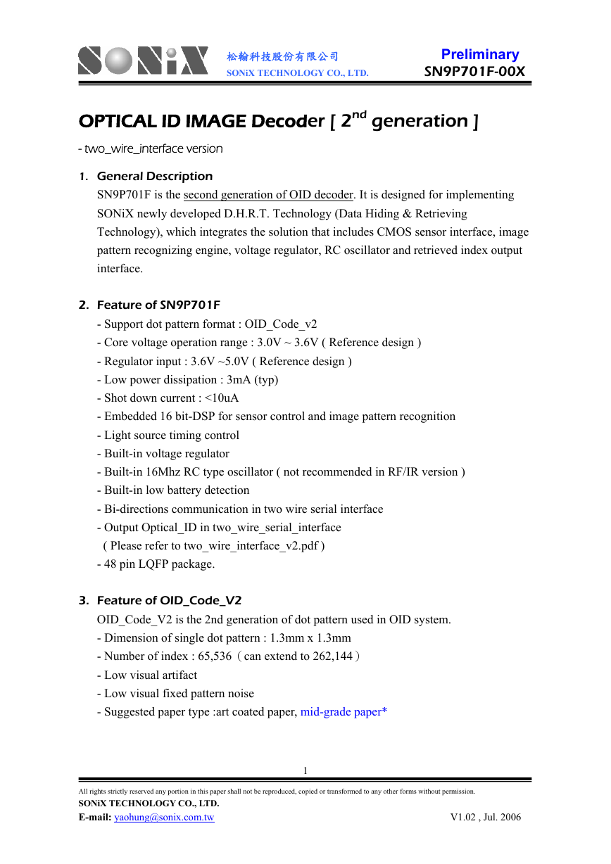
SN9P701F is the second generation of OID decoder. It is designed for implementing
SONiX newly developed D.H.R.T. Technology (Data Hiding & Retrieving
Technology), which integrates the solution that includes CMOS sensor interface, image
pattern recognizing engine, voltage regulator, RC oscillator and retrieved index output
interface.
2. Feature of SN9P701F
- Support dot pattern format : OID_Code_v2
- Core voltage operation range : 3.0V ~ 3.6V ( Reference design )
- Regulator input : 3.6V ~5.0V ( Reference design )
- Low power dissipation : 3mA (typ)
- Shot down current : <10uA
- Embedded 16 bit-DSP for sensor control and image pattern recognition
- Light source timing control
- Built-in voltage regulator
- Built-in 16Mhz RC type oscillator ( not recommended in RF/IR version )
- Built-in low battery detection
- Bi-directions communication in two wire serial interface
- Output Optical_ID in two_wire_serial_interface
( Please refer to two_wire_interface_v2.pdf )
- 48 pin LQFP package.
3. Feature of OID_Code_V2
OID_Code_V2 is the 2nd generation of dot pattern used in OID system.
- Dimension of single dot pattern : 1.3mm x 1.3mm
- Number of index : 65,536(can extend to 262,144)
- Low visual artifact
- Low visual fixed pattern noise
- Suggested paper type :art coated paper, mid-grade paper*
All rights strictly reserved any portion in this paper shall not be reproduced, copied or transformed to any other forms without permission.
SONiX TECHNOLOGY CO., LTD.
E-mail: yaohung@sonix.com.tw
1
V1.02 , Jul. 2006
�
松翰科技股份有限公司 Preliminary
SONiX TECHNOLOGY CO., LTD. SN9P701F-00X
4. Specification of 2nd generation OID decoding system
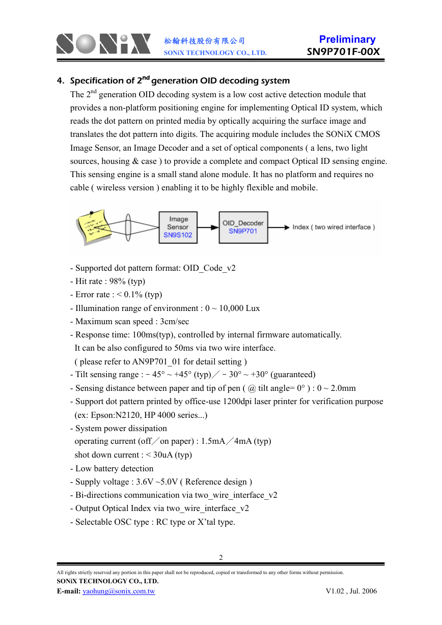
The 2nd generation OID decoding system is a low cost active detection module that
provides a non-platform positioning engine for implementing Optical ID system, which
reads the dot pattern on printed media by optically acquiring the surface image and
translates the dot pattern into digits. The acquiring module includes the SONiX CMOS
Image Sensor, an Image Decoder and a set of optical components ( a lens, two light
sources, housing & case ) to provide a complete and compact Optical ID sensing engine.
This sensing engine is a small stand alone module. It has no platform and requires no
cable ( wireless version ) enabling it to be highly flexible and mobile.
- Supported dot pattern format: OID_Code_v2
- Hit rate : 98% (typ)
- Error rate : < 0.1% (typ)
- Illumination range of environment : 0 ~ 10,000 Lux
- Maximum scan speed : 3cm/sec
- Response time: 100ms(typ), controlled by internal firmware automatically.
It can be also configured to 50ms via two wire interface.
( please refer to AN9P701_01 for detail setting )
- Tilt sensing range :–45° ~ +45° (typ)/–30° ~ +30° (guaranteed)
- Sensing distance between paper and tip of pen ( @ tilt angle= 0° ) : 0 ~ 2.0mm
- Support dot pattern printed by office-use 1200dpi laser printer for verification purpose
(ex: Epson:N2120, HP 4000 series...)
- System power dissipation
operating current (off/on paper) : 1.5mA/4mA (typ)
shot down current : < 30uA (typ)
- Low battery detection
- Supply voltage : 3.6V ~5.0V ( Reference design )
- Bi-directions communication via two_wire_interface_v2
- Output Optical Index via two_wire_interface_v2
- Selectable OSC type : RC type or X’tal type.
All rights strictly reserved any portion in this paper shall not be reproduced, copied or transformed to any other forms without permission.
SONiX TECHNOLOGY CO., LTD.
E-mail: yaohung@sonix.com.tw
2
V1.02 , Jul. 2006
�
松翰科技股份有限公司 Preliminary
SONiX TECHNOLOGY CO., LTD. SN9P701F-00X
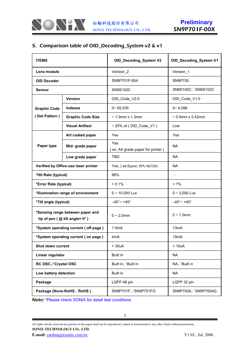
5. Comparison table of OID_Decoding_System v2 & v1
ITEMS
Lens module
OID Decoder
Sensor
Graphic Code
( Dot Pattern )
OID_Decoding_System V2
OID_Decoding_System V1
Version_2
SN9P701F-004
SN9S102C
OID_Code_V2.0
0~ 65,535
Version_1
SN9P700
SN9S100C/SN9S102C
OID_Code_V1.0
0~ 4,096
Version
Indexes
Graphic Code Size
~ 1.3mm x 1.3mm
~ 0.5mm x 0.42mm
Visual Artifact
~ 25% of ( OID_Code_V1 )
Art coated paper
Yes
Paper type
Mid- grade paper
Low grade paper
Yes
( ex: A4 grade paper for printer )
TBD
Verified by Office-use laser printer
Yes, ( ex:Epson, EPL-N2120)
*Hit Rate (typical)
*Error Rate (typical)
98%
< 0.1%
*Illumination range of environment
0 ~ 10,000 Lux
*Tilt angle (typical)
*Sensing range between paper and
tip of pen ( @ tilt angle= 0° )
–45°~ +45°
0 ~ 2.0mm
*System operating current ( off page )
1.5mA
*System operating current ( on page )
4mA
Shot down current
Linear regulator
RC OSC/Crystal OSC
Low battery detection
Package
< 30uA
Built in
Built in/Built in
Built in
LQFP 48 pin
Low
Yes
NA
NA
NA
─
< 1%
0 ~ 3,000 Lux
–40°~ +40°
0 ~ 1.0mm
13mA
15mA
< 10uA
NA
NA/Built in
NA
LQFP 32 pin
Package (None-RoHS/RoHS )
SN9P701F/SN9P701FG
SN9P700A/SN9P700AG
Note: *Please check SONiX for detail test conditions
All rights strictly reserved any portion in this paper shall not be reproduced, copied or transformed to any other forms without permission.
SONiX TECHNOLOGY CO., LTD.
E-mail: yaohung@sonix.com.tw
3
V1.02 , Jul. 2006
�
松翰科技股份有限公司 Preliminary
SONiX TECHNOLOGY CO., LTD. SN9P701F-00X
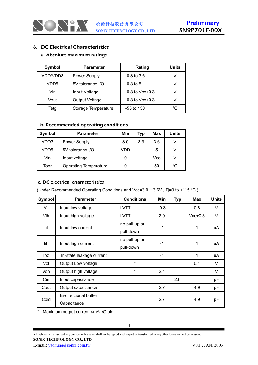
6. DC Electrical Characteristics
a. Absolute maximum ratings
Symbol
VDD/VDD3
VDD5
Vin
Vout
Tstg
Parameter
Rating
Units
Power Supply
5V tolerance I/O
Input Voltage
Output Voltage
Storage Temperature
-0.3 to 3.6
-0.3 to 5
-0.3 to Vcc+0.3
-0.3 to Vcc+0.3
-55 to 150
V
V
V
V
°C
Parameter
b. Recommended operating conditions
Min
Symbol
VDD3
3.0
VDD
VDD5
0
Vin
Topr
0
Power Supply
5V tolerance I/O
Input voltage
Operating Temperature
Typ Max
3.3
3.6
5
Vcc
50
Units
V
V
V
°C
c. DC electrical characteristics
(Under Recommended Operating Conditions and Vcc=3.0 ~ 3.6V , Tj=0 to +115 °C )
Symbol
Parameter
Conditions
Vil
Vih
Iil
Input low voltage
Input high voltage
Input low current
Iih
Input high current
Ioz
Vol
Voh
Cin
Cout
Cbid
Tri-state leakage current
Output Low voltage
Output high voltage
Input capacitance
Output capacitance
Bi-directional buffer
Capacitance
LVTTL
LVTTL
no pull-up or
pull-down
no pull-up or
pull-down
*
*
* : Maximum output current 4mA I/O pin .
Min
-0.3
2.0
-1
-1
-1
2.4
2.7
2.7
Typ
2.8
Max
0.8
Vcc+0.3
Units
V
V
1
1
1
0.4
4.9
4.9
uA
uA
uA
V
V
pF
pF
pF
All rights strictly reserved any portion in this paper shall not be reproduced, copied or transformed to any other forms without permission.
SONiX TECHNOLOGY CO., LTD.
E-mail: yaohung@sonix.com.tw
4
V0.1 , JAN. 2003
�
松翰科技股份有限公司 Preliminary
SONiX TECHNOLOGY CO., LTD. SN9P701F-00X
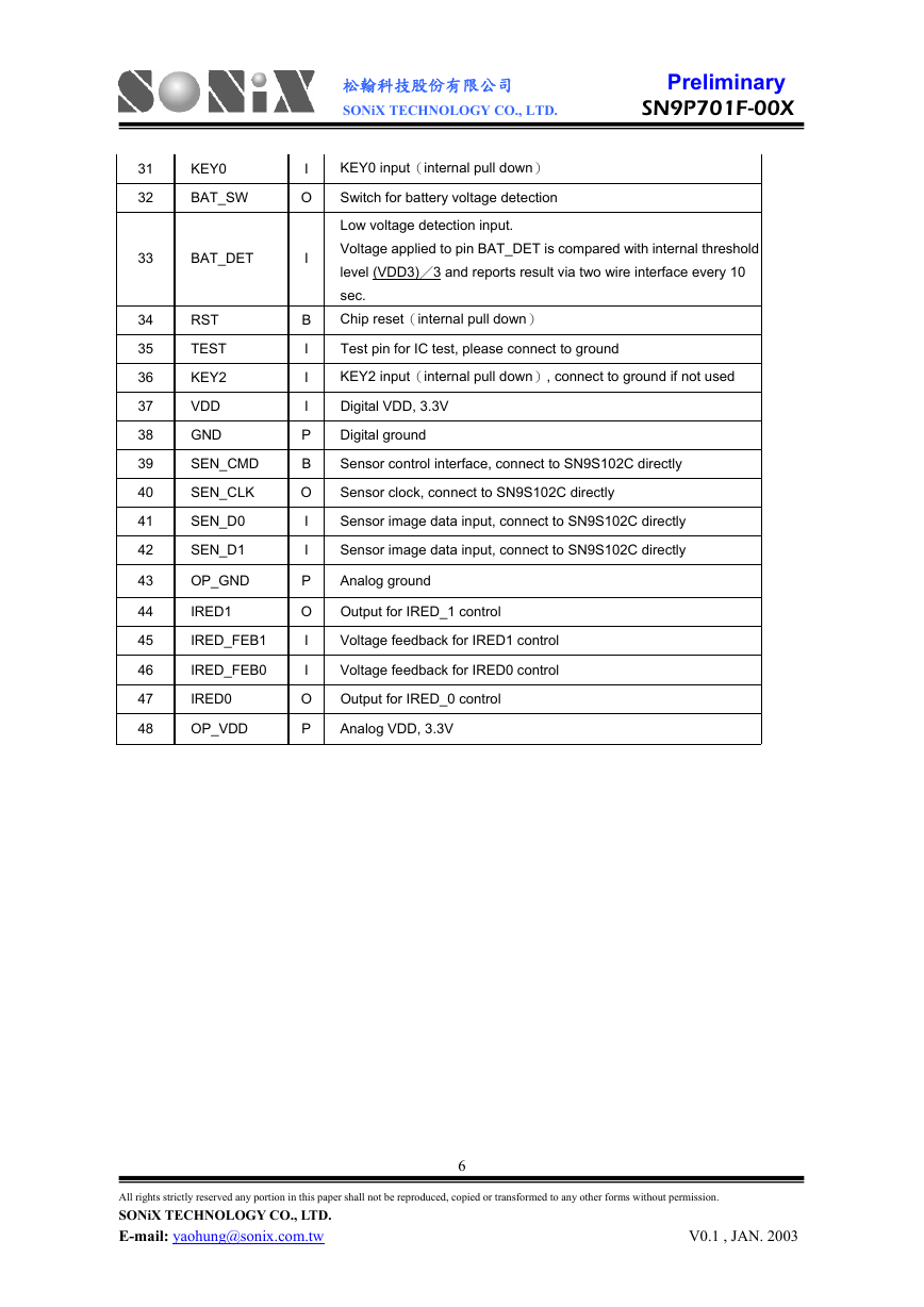
6. Pin Assignment
LQFP
48
PIN NAME
Type
Description
1
2
3
4
5
6
7
8
9
10
11
12
13
14
15
16
17
18
19
20
21
22
23
24
25
26
27
28
29
30
KEY1
GPIO0
GPIO1
GPIO2
VDD3
GND
GPIO3
ADIO2
ADIO0
VSSD_OSC
RC_BIAS
VDD_OSC
XIN
XOUT
XTAL_SEL
VDD3
GND
TAVSS
DN
DP
TAVDD
VRO_S
VRO_P
GND_A
REG_IN
REG_EN
PWR_CTL
VDD5D
ADIO1
USB_DET
I
B
B
B
P
P
B
B
B
P
P
P
I
B
I
P
P
P
B
B
P
O
O
P
P
I
O
P
B
I
KEY1 input(internal pull down), connect to ground if no used
General purpose I/O
General purpose I/O
General purpose I/O
Digital VDD, 3.3V
Digital ground
General purpose I/O
ADIO2/ADO_SDIO/IR_TRAN/RF_TRAN
ADIO0/ADO_CLK
GND for oscillator
RC oscillator bias, using an external “R” to set frequency.
Recommended “R” = 29KΩ±1% for 16MHz ±10% frequency.
VDD for oscillator, 3.3V
Crystal OSC input
Crystal OSC output
OSC type selection ( 1:Crystal, 0:RC )
Digital VDD, 3.3V
GND for I/O and core
Reserved, please connect to digital GND
Reserved, please connect 5KΩ to digital GND
Reserved, please connect 5KΩ to digital VDD, 3.3V
Reserved, please connect to digital VDD, 3.3V
Regulator 3.3 v switch output, controlled by internal firmware
Regulator 3.3 v output, controlled by REG_EN
Analog ground
Regulator input , 3.6V~5V
Regulator enable
Output for power control
Digital VDD, VDD3 ~ 5V, please do not connect to VRO_P
ADIO1/ADO_SCK
Reserved, please connect to ground
All rights strictly reserved any portion in this paper shall not be reproduced, copied or transformed to any other forms without permission.
SONiX TECHNOLOGY CO., LTD.
E-mail: yaohung@sonix.com.tw
5
V0.1 , JAN. 2003
�
松翰科技股份有限公司 Preliminary
SONiX TECHNOLOGY CO., LTD. SN9P701F-00X
KEY0 input(internal pull down)
Switch for battery voltage detection
Low voltage detection input.
Voltage applied to pin BAT_DET is compared with internal threshold
level (VDD3)/3 and reports result via two wire interface every 10
sec.
Chip reset(internal pull down)
Test pin for IC test, please connect to ground
KEY2 input(internal pull down), connect to ground if not used
Digital VDD, 3.3V
Digital ground
Sensor control interface, connect to SN9S102C directly
Sensor clock, connect to SN9S102C directly
Sensor image data input, connect to SN9S102C directly
Sensor image data input, connect to SN9S102C directly
Analog ground
Output for IRED_1 control
Voltage feedback for IRED1 control
Voltage feedback for IRED0 control
Output for IRED_0 control
Analog VDD, 3.3V
31
32
KEY0
BAT_SW
33
BAT_DET
34
35
36
37
38
39
40
41
42
43
44
45
46
47
48
RST
TEST
KEY2
VDD
GND
SEN_CMD
SEN_CLK
SEN_D0
SEN_D1
OP_GND
IRED1
IRED_FEB1
IRED_FEB0
IRED0
OP_VDD
I
O
I
B
I
I
I
P
B
O
I
I
P
O
I
I
O
P
All rights strictly reserved any portion in this paper shall not be reproduced, copied or transformed to any other forms without permission.
SONiX TECHNOLOGY CO., LTD.
E-mail: yaohung@sonix.com.tw
6
V0.1 , JAN. 2003
�
松翰科技股份有限公司 Preliminary
SONiX TECHNOLOGY CO., LTD. SN9P701F-00X
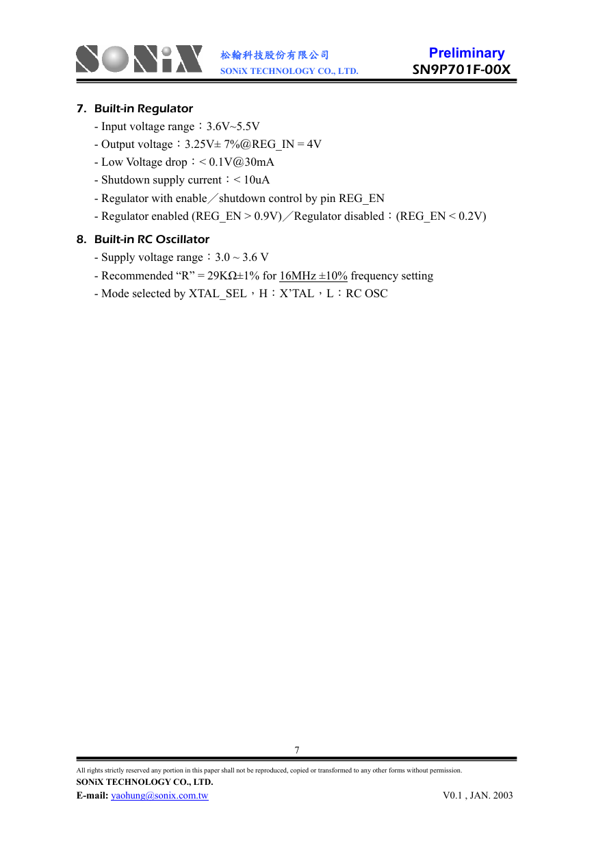
7. Built-in Regulator
- Input voltage range:3.6V~5.5V
- Output voltage:3.25V± 7%@REG_IN = 4V
- Low Voltage drop:< 0.1V@30mA
- Shutdown supply current:< 10uA
- Regulator with enable/shutdown control by pin REG_EN
- Regulator enabled (REG_EN > 0.9V)/Regulator disabled:(REG_EN < 0.2V)
8. Built-in RC Oscillator
- Supply voltage range:3.0 ~ 3.6 V
- Recommended “R” = 29KΩ±1% for 16MHz ±10% frequency setting
- Mode selected by XTAL_SEL,H:X’TAL,L:RC OSC
All rights strictly reserved any portion in this paper shall not be reproduced, copied or transformed to any other forms without permission.
SONiX TECHNOLOGY CO., LTD.
E-mail: yaohung@sonix.com.tw
7
V0.1 , JAN. 2003
�
松翰科技股份有限公司 Preliminary
SONiX TECHNOLOGY CO., LTD. SN9P701F-00X
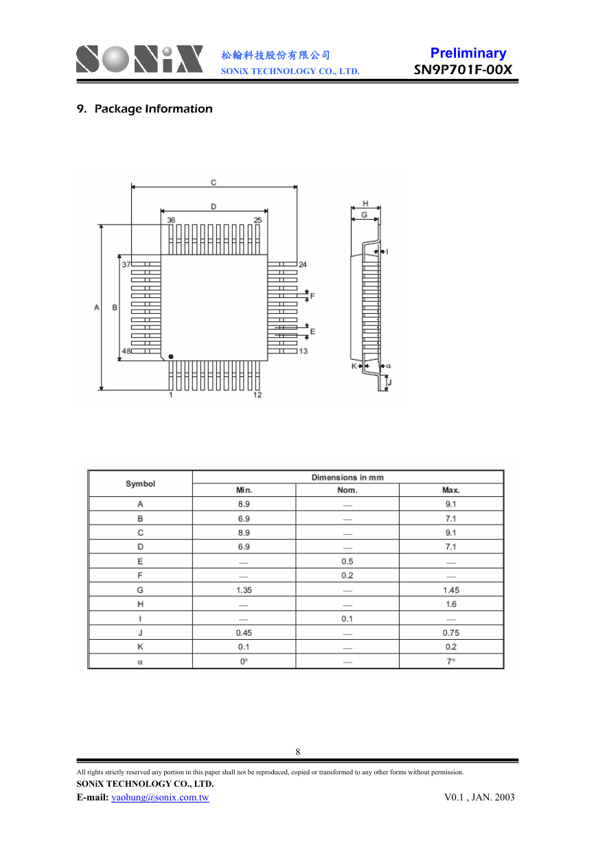
9. Package Information
All rights strictly reserved any portion in this paper shall not be reproduced, copied or transformed to any other forms without permission.
SONiX TECHNOLOGY CO., LTD.
E-mail: yaohung@sonix.com.tw
8
V0.1 , JAN. 2003
�



 2023年江西萍乡中考道德与法治真题及答案.doc
 2012年重庆南川中考生物真题及答案.doc
 2013年江西师范大学地理学综合及文艺理论基础考研真题.doc
 2020年四川甘孜小升初语文真题及答案I卷.doc
 2020年注册岩土工程师专业基础考试真题及答案.doc
 2023-2024学年福建省厦门市九年级上学期数学月考试题及答案.doc
 2021-2022学年辽宁省沈阳市大东区九年级上学期语文期末试题及答案.doc
 2022-2023学年北京东城区初三第一学期物理期末试卷及答案.doc
 2018上半年江西教师资格初中地理学科知识与教学能力真题及答案.doc
 2012年河北国家公务员申论考试真题及答案-省级.doc
 2020-2021学年江苏省扬州市江都区邵樊片九年级上学期数学第一次质量检测试题及答案.doc
 2022下半年黑龙江教师资格证中学综合素质真题及答案.doc